EP0264127A2 - Magnetron device - Google Patents
Magnetron device Download PDFInfo
- Publication number
- EP0264127A2 EP0264127A2 EP87115063A EP87115063A EP0264127A2 EP 0264127 A2 EP0264127 A2 EP 0264127A2 EP 87115063 A EP87115063 A EP 87115063A EP 87115063 A EP87115063 A EP 87115063A EP 0264127 A2 EP0264127 A2 EP 0264127A2
- Authority
- EP
- European Patent Office
- Prior art keywords
- anode cylinder
- vanes
- antenna
- magnetron device
- anode
- Prior art date
- Legal status (The legal status is an assumption and is not a legal conclusion. Google has not performed a legal analysis and makes no representation as to the accuracy of the status listed.)
- Granted
Links
Images


Classifications
-
- H—ELECTRICITY
- H01—ELECTRIC ELEMENTS
- H01J—ELECTRIC DISCHARGE TUBES OR DISCHARGE LAMPS
- H01J23/00—Details of transit-time tubes of the types covered by group H01J25/00
- H01J23/16—Circuit elements, having distributed capacitance and inductance, structurally associated with the tube and interacting with the discharge
- H01J23/18—Resonators
- H01J23/22—Connections between resonators, e.g. strapping for connecting resonators of a magnetron
-
- H—ELECTRICITY
- H01—ELECTRIC ELEMENTS
- H01J—ELECTRIC DISCHARGE TUBES OR DISCHARGE LAMPS
- H01J23/00—Details of transit-time tubes of the types covered by group H01J25/00
- H01J23/36—Coupling devices having distributed capacitance and inductance, structurally associated with the tube, for introducing or removing wave energy
- H01J23/40—Coupling devices having distributed capacitance and inductance, structurally associated with the tube, for introducing or removing wave energy to or from the interaction circuit
- H01J23/48—Coupling devices having distributed capacitance and inductance, structurally associated with the tube, for introducing or removing wave energy to or from the interaction circuit for linking interaction circuit with coaxial lines; Devices of the coupled helices type
Definitions
- the present invention generally relates to a magnetron device and more particularly, to an improved magnetron to be incorporated in a high frequency microwave oven i.e. so-called electronic range or the like (referred to as an electronic range hereinafter).
- a ferrite magnet In the magnetron commonly used, a ferrite magnet has been generally employed, and it was considered to replace the material for the magnet by Alnico (name used in trade and manufactured by General Electric Co., U.S.A.) or a samarium-cobalt (Sm-Co)alloy for reduction of size and weight of the magnetic circuit.
- Alnico name used in trade and manufactured by General Electric Co., U.S.A.
- Sm-Co samarium-cobalt
- a magnetron output structure For other means to achieve the above first subject through employment of the ferrite magnet, there may be considered an improvement of a magnetron output structure. More specifically, in the magnetron for common use, although the output antenna is arranged in the axial direction of an anode cylinder, it is intended, in the improved structure, to dispose the output antenna in a direction normal or perpendicular to the axis of the anode cylinder.
- the advantage of the above structure is such that the structural dimension of the magnetron main body with respect to the longitudinal direction of its output antenna can be reduced, whereby compact size of the electronic range on the whole may be achieved.
- the ratio of the cathode radius r c to the anode inner radius r a is designed to satisfy the relation represented by with respect to the number of resonance cavities N in order to achieve a stable ⁇ mode oscillation.
- this is dealt with by devising configurations of pole pieces disposed at opposite ends in the axial direction of the interaction space.
- the latter means is introduced into the resonance circuit as designed by the former means.
- noises are increased in proportion to the increase of the coupling degree, and thus, although the practice involves some inconsistency with respect to the requirement for low noise which is another subject for improvement to be described below, the optimum coupling degree has been selected while suppressing the noise within the standard.
- the magnetron structure disclosed in said prior art is mainly characterized in a supporting construction of the cathode position, in which said cathode portion is arranged to be supported by a pair of pole pieces insulated from the anode portion.
- a set of strap rings are arranged at the central portion in the axial direction of an anode cylinder within the vanes, while an output antenna is disposed in a direction normal to the axis of the anode cylinder as a third feature.
- an essential object of the present invention is to provide a magnetron device compact in size at high operating efficiency with a low noise, and can be readily manufactured at the same cost as in the conventional magnetron devices.
- Another important object of the present invention is to provide a magnetron device of the above described type, which is provided, inside its vanes, with improved strap rings whose effects for reduction of noise have been clarified.
- a further object of the present invention is to provide a magnetron device of the above described type, which is provided with an improved output structure in the construction having an output antenna disposed normal to the axis of an anode cylinder.
- Still another object of the present invention is to provide a magnetron device which is so constructed that the above improved output structure may be manufactured at high accuracy.
- a magnetron device which includes an anode cylinder, a plurality of vanes radially arranged within the anode cylinder, a set of strap rings with different diameters, arranged through holes in the vanes so as to be alternately connected to the vanes, an output antenna portion disposed in a direction normal to an axis of the anode cylinder, an antenna lead having its one end connected to the strap ring, and the other end thereof extended through a coupling hole formed in a side wall of the anode cylinder so as to be held and fixed within the output antenna portion for example, by brazing, and an exhaust pipe provided on one end face of the anode cylinder for evacuation of the interior of said anode cylinder.
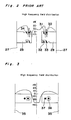
- FIG. 1 a general construction of one example of a conventional magnetron device.
- the known magnetron device of Fig. 1 generally includes an anode cylinder 1, a plurality of vanes 2 disposed within said anode cylinder 1, two sets of strap rings 3 provided at opposite ends of the vanes 2 in an axial direction of said anode cylinder 1, and each alternately connected to every other vane of said plurality of vanes 2, and an antenna lead 4 having its one end connected to any one of the vanes 2 at a desired position, and its other end extending up to an antenna portion 7 disposed in the axial direction of the anode cylinder 1 through a coupling hole 6 of a pole piece 5 provided at the end of the anode cylinder 1.
- the magnetron device further includes a cathode portion 9 composed of a spirally wound filament concentrically disposed with the anode cylinder 1 at the central portion of said anode cylinder, with end plates 10 and 11 provided at opposite ends of said cathode portion 9.
- the end plates 10 and 11 are respectively connected to support leads 12 and 13 disposed in the axial direction of the anode cylinder 1, while the respective support leads 12 and 13 are connected to a cathode stem 14 of a ceramic material disposed at the end face of the anode cylinder 1 on the side opposite to the output antenna portion 7, for example, by silver-copper alloy brazing, and this cathode stem 14 is fixed to the end face of the anode cylinder 1 through a cathode side pipe 15 connected thereto also by silver-copper alloy brazing.
- FIG. 1 There are also provided another pole piece 16 at the side of the cathode stem 14, a dielectric member 17 and a metallic pipe 18 for suppressing unnecessary radiation toward the cathode stem 14, ferrite permanent magnets 19 and 20 disposed at the opposite sides of the end faces of said anode cylinder 1, heat radiating fins 21 forcibly fitted around the anode cylinder 1, yokes 22 and 23 for constituting a magnetic circuit, a choke coil 24 with a core connected at its one end to the cathode stem 14 and at its other end to a capacitor 25 extended into a filter box 26 covering the portion of the cathode stem 14 and the choke coil 24.
- one measure for enhancing the output efficiency of the magnetron is to dispose the connecting position of the antenna lead 4 with the specific vane 2 towards the central portion of the anode cylinder 1 as far as practicable.
- such connecting position is limited from the viewpoint of structure, since the strap rings are disposed at the vane end portions.
- the conventional magnetron device has the construction capable of simultaneously satisfying both requirements for the high output efficiency and suppression of unnecessary radiation.
- Fig. 2 shows a diagram representing the high frequency electric field distribution at the vane side end face in the conventional magnetron anode construction as measured by the present inventors.
- the inner wall of the anode cylinder 1 is represented by Numeral 27
- vanes confronting each other within the anode cylinder 1 are shown by Numerals 28 and 29
- strap rings are denoted by Numerals 30, 31, 32 and 33
- portion where the antenna lead is connected is indicated by Numeral 34. From this diagram, it is noticed that, in the conventional structure in which the strap rings are disposed at the vane side end portions, the high-frequency electric field is disturbed to a large extent in the vicinity of the strap rings.
- the first point is that the high frequency field distribution on the vane side end face is in good order, while the second point relates to the fact that since the high frequency field distribution is generally symmetrical with respect to the cylinder axis and thus, the high frequency electric field intensity is extremely low in the space located between the confronting vanes, coupling of the microwave energy with respect to the cathode portion is weak.
- the anode structure as described above movement of electrons is not readily disturbed by the microwaves, and it is considered that the suppression of the unnecessary radiation which leaks through coupling with the cathode electrode will be remarkably improved.
- the output structure disclosed in the above U.S. Patent i.e. the microwave energy deriving structure in which one end of the antenna lead is formed into a loop shape, with its forward end connected to the vane has such a disadvantage that it is difficult to enhance the efficiency of the magnetron up to the efficiency obtainable by the conventional output deriving structure as shown in Fig. 1, and this drawback is attributable to the construction of the set of strap rings. More specifically, as is well known, to the determination of the resonance frequency of the small resonance cavity defined by the neighboring vanes and the inner side face of the anode cylinder, inductance Lr and capacitance Cr of the cavity when the presence of strap rings is neglected, and capacitance Cs generated by attaching the strap rings are related.
- the ratio of the capacitance Cr to capacitance Cs should be properly determined from the view point of oscillation mode separating degree.
- the strap rings is required to have a diameter larger than that in the conventional arrangement. Therefore, the connecting position of the antenna lead to the vane is undesirably shifted towards the inner wall face side of the anode cylinder to a larger extent than in the conventional arrangement, thus inviting reduction of efficiency due to lowering in the coupling degree.
- the antenna lead may be prolonged as one measure, but since such prolongation can only be accomplished outside the anode cylinder due to the reason as described earlier, this means to prolong the output antenna portion consequently, thus making it necessary to adopt a structure contrary to the tendency towards the compact size or to employ an unpractical construction.
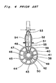
- the present inventors proposed an arrangement for directly connecting the antenna lead to the strap rings, one example of which is shown in Fig. 4.
- the known magnetron device of Fig. 4 includes an anode cylinder 38, a plurality of vanes 39 to 48 radially arranged in the anode cylinder 38, a set of strap rings 49 and 50 alternately connected to every other vane of said vanes, an antenna side pipe 51 extending outwardly from the anode cylinder 38 in a direction perpendicular to the axis of said anode cylinder, a ceramic side pipe 52 connected to the antenna side pipe 51, for example, by silver-copper brazing, an exhaust pipe 53 connected to the ceramic side pipe 52 also by silver-copper brazing or the like, and an antenna lead 54 concentrically disposed through a coupling hole 55 of the anode cylinder 38, the antenna side pipe 51, the ceramic side pipe 52 and the exhaust pipe 53 so as to be connected at its one end to the strap ring 49 and fixed at a sealed cut portion in its other end cut off together with the exhaust pipe 53 after evacuation of the interior of the anode cylinder 38 up to a predetermined level.
- the portion represented by one-dot chain lines shows the exhaust pipe and antenna lead before the cutting, and is to be depressed for cutting in the directions indicated by arrows.
- the antenna lead 54 is pushed towards the anode cylinder 38 by the volume variation component thereof due to the depression for cutting, thus resulting in deformation of the strap ring 49 connected to the antenna lead 54 towards the central portion of the anode cylinder 38 or bending of the vane 39 connected with the strap ring toward the neighboring vane 40 by the stress during the cutting, or contact between the strap rings or vanes in the worst case, thereby hindering normal operation of the magnetron device.
- FIGs. 5 and 6 there is shown an improved magnetron device according to one preferred embodiment of the present invention in which the problems in the conventional magnetron devices have been eliminated.
- the magnetron device of the present invention generally includes an anode cylinder 56, a plurality of vanes 57 radially disposed within the anode cylinder 56, a set of strap rings 58 and 59 having different diameters and disposed, through holes in the vanes, on the same plane generally at the central portion in the axial direction of the anode cylinder 56 so as to be alternately connected to every other vane of said plurality of vanes 57, an antenna lead 60 connected, at its one end, to the strap ring 59 with the larger diameter, generally at an intermediate portion of the ring between the neighboring vanes (the vanes 57a and 57b in Fig. 6) of the plurality of vanes.
- the above antenna lead 60 extends outwardly from the portion connected with the strap ring 59 in a direction perpendicular to the axis of the anode cylinder 56 through a coupling hole 61 formed in the side face of the anode cylinder 56 so as to reach an output antenna portion 62 as shown.
- a cathode portion 63 composed of a spiral-form filament and concentrically disposed at the central portion of the anode cylinder 56, with end plates 64 and 65 being mounted at opposite ends of said cathode portion 63 and respectively connected to support leads 66 and 67 disposed in the axial direction of the anode cylinder 56.
- These support leads 66 and 67 are connected to a cathode stem 68 of a ceramic material provided at one end face side of the anode cylinder 56, for example, by silver-copper alloy brazing so as to be supported thereby.
- This cathode stem 68 is welded onto the end face of the anode cylinder 56 via a cathode side pipe 69 connected thereto, for example, also by silver-copper alloy brazing.
- an exhaust pipe 70 is disposed so as to be cut and sealed as shown after evacuation of the interior of the anode cylinder 56.
- the output antenna portion 62 is composed of a ceramic side pipe 71, an antenna portion sealing pipe 72 and an antenna cap 73, with one end of the antenna lead 60 being brazed to the antenna portion sealing pipe 72.
- the magnetron device further includes pole pieces 74 and 75, ferrite permanent magnets 76 and 77, yokes 78 and 79 for constituting the magnetic circuit, heat radiating fins 80 fitted over the anode cylinder 56 under pressure, heat insulating plates 81 and 82 each provided between the anode cylinder 56 and the permanent magnets 76 and 77 for insulating the permanent magnets from the heat radiation from the anode cylinder, a filter box 83, choke coils 84 and a through-capacitor 85, etc.
- the output antenna portion 62 is mounted on the side wall of the anode cylinder through a first metallic pipe 86 and a second metallic pipe 87.
- Each of these first and second metallic pipes 86 and 87 has a flange portion at its one end so as to be connected to each other at the outer peripheries of the flange portions, for example, by welding.
- a disc-like metallic plate 89 is assembled so as to dispose a metallic gasket 88 thereon, and this metallic gasket 88 is fixed and supported at the base portion of the output antenna 62 by the metallic plate 89 and the yoke 79.
- the antenna lead may be fixed in the predetermined state of disposition before the exhaust process, while the undesirable deformation of the strap rings and vanes, etc. at the cutting and sealing process of the exhaust pipe can be eliminated.
- the configuration of the antenna portion sealing pipe may be so modified as to provide a portion for supporting and fixing the antenna lead at the side of said pipe, and that the inner diameter of the exhaust pipe may be increased up to approximately the inner diameter of the cathode stem shown in the drawing for expediting evacuation of the interior of the anode cylinder.
Abstract
Description
- The present invention generally relates to a magnetron device and more particularly, to an improved magnetron to be incorporated in a high frequency microwave oven i.e. so-called electronic range or the like (referred to as an electronic range hereinafter).
- In the field of electronic ranges which are coming into wide use in recent years, technical improvements have been continuously made in order to achieve the targets and satisfy the requirements both in the demand and supply with respect to compact size, light weight and reduction in cost, and under the above circumstances, reduction in size and weight, high operating efficiency, low noise and reduction of cost, etc. are also required for the magnetron to be incorporated in such electronic range.
- With respect to the compact size and light weight which are of the first subject, improvement of a magnetic circuit is first brought into consideration.
- In the magnetron commonly used, a ferrite magnet has been generally employed, and it was considered to replace the material for the magnet by Alnico (name used in trade and manufactured by General Electric Co., U.S.A.) or a samarium-cobalt (Sm-Co)alloy for reduction of size and weight of the magnetic circuit. However, such magnet material could not take the place of the ferrite magnet due to a strong market tendency towards the low cost.
- For other means to achieve the above first subject through employment of the ferrite magnet, there may be considered an improvement of a magnetron output structure. More specifically, in the magnetron for common use, although the output antenna is arranged in the axial direction of an anode cylinder, it is intended, in the improved structure, to dispose the output antenna in a direction normal or perpendicular to the axis of the anode cylinder. The advantage of the above structure is such that the structural dimension of the magnetron main body with respect to the longitudinal direction of its output antenna can be reduced, whereby compact size of the electronic range on the whole may be achieved.
- With respect to the high operating efficiency which is the second subject for the improvement, owing to the fact that this efficiency is to be determined by the product of electronic efficiency, which is a conversion factor for converting kinetic energy of electrons emitted from a cathode into high frequency energy, and circuit efficiency, which is a deriving factor for deriving the high frequency energy produced in a resonance circuit of an anode out of the anode, such improvement of the operating efficiency may be ascribed to enhancement of the electronic efficiency or circuit efficiency.
- As means for enhancing the electronic efficiency, there may be considered optimization of a relative construction of the cathode portion diameter and the inner diameter of the anode surrounding the cathode portion with respect to the number of resonance cavities of the anode resonance circuit, i.e. optimization of an interaction space, uniform distribution of magnetic field within said interaction space, and optimization of action of the high frequency field into the interaction space, i.e. optimization of the high frequency field action with respect to electrons.
- Of the above means, with respect to the former two means, various studies have been made up to the present, with the technique therefor being almost established. By way of example, for the optimization of the interaction space, the ratio of the cathode radius rc to the anode inner radius ra is designed to satisfy the relation represented by

- However, concerning the optimization of the high frequency field action with respect to electrons, there has been no technique which clearly refers thereto as a structure for the means, about which, description will be given later.
- On the other hand, as means for improving the circuit efficiency, there may be conceived enhancement of a value Q for the resonance circuit, i.e. reduction of loss in the resonance cavities, increase of coupling degree between a load circuit and the resonance circuit, etc.
- Normally, the latter means is introduced into the resonance circuit as designed by the former means. Incidentally, noises are increased in proportion to the increase of the coupling degree, and thus, although the practice involves some inconsistency with respect to the requirement for low noise which is another subject for improvement to be described below, the optimum coupling degree has been selected while suppressing the noise within the standard.
- With respect to the reduction of noise related to the third subject, most of the means employed are arranged to suppress the generated noise by a filter circuit added thereto, but there have also been considered some means adapted to suppress generation of the noise itself. By way of example, there are proposed means for suppressing noise through suppression of turbulence in the electron movement near the forward end side portions of vanes which form the resonance cavity group, by applying proper cuts in the edge in the longitudinal direction of such vane forward end side portions confronting the cathode portion, and means for suppressing noise through suppression of electron flow intending to flow out in the longitudinal direction of the cathode portion by insulating the pole pieces disposed at the opposite ends in the axial direction of the interaction space, from the anode portion.
- For solving the various subjects as described so far, there has conventionally been disclosed an interesting construction, for example, in U.S. Patent No. 4,310,786. The magnetron structure disclosed in said prior art is mainly characterized in a supporting construction of the cathode position, in which said cathode portion is arranged to be supported by a pair of pole pieces insulated from the anode portion. As a second feature, a set of strap rings are arranged at the central portion in the axial direction of an anode cylinder within the vanes, while an output antenna is disposed in a direction normal to the axis of the anode cylinder as a third feature. Accordingly, with respect to the various subjects as described earlier, the construction of said prior art intends to achieve compact size and low noise, although the operating efficiency thereof is considered to be lower than that of the conventional magnetron due to a reason which is to be described later.
- Regarding the construction of the strap rings which is the second feature of the above described prior art, there are also considered various other constructions, part of which is disclosed, for example, in U.S. Patent No. 3,553,524. In this prior art, it is stated that the position for disposing the strap rings for stably maintaining the π mode oscillation should preferably be within the vanes as compared with the arrangement of such strap rings at upper and lower edges of vanes as employed in the common magnetrons. Meanwhile, it is shown that the strap ring arranging construction in U.S. Patent No. 4,310,786 referred to earlier is difficult to be applied to the commonly used magnetrons due to increase of manufacturing cost, but this point may be solved if the techniques disclosed in U.S. Patent Nos. 4,056,756 and 4,179,639 are adopted.
- In connection with the above, it is to be noted that, with respect to the effects in use of such strap rings to be arranged within the vanes, specific effects thereof have not been fully clarified up to the present.
- Accordingly, an essential object of the present invention is to provide a magnetron device compact in size at high operating efficiency with a low noise, and can be readily manufactured at the same cost as in the conventional magnetron devices.
- Another important object of the present invention is to provide a magnetron device of the above described type, which is provided, inside its vanes, with improved strap rings whose effects for reduction of noise have been clarified.
- A further object of the present invention is to provide a magnetron device of the above described type, which is provided with an improved output structure in the construction having an output antenna disposed normal to the axis of an anode cylinder.
- Still another object of the present invention is to provide a magnetron device which is so constructed that the above improved output structure may be manufactured at high accuracy.
- In accomplishing these and other objects, according to one preferred embodiment of the present invention, there is provided a magnetron device which includes an anode cylinder, a plurality of vanes radially arranged within the anode cylinder, a set of strap rings with different diameters, arranged through holes in the vanes so as to be alternately connected to the vanes, an output antenna portion disposed in a direction normal to an axis of the anode cylinder, an antenna lead having its one end connected to the strap ring, and the other end thereof extended through a coupling hole formed in a side wall of the anode cylinder so as to be held and fixed within the output antenna portion for example, by brazing, and an exhaust pipe provided on one end face of the anode cylinder for evacuation of the interior of said anode cylinder.
- By the above arrangement of the present invention, a compact magnetron device with high operating efficiency and low noise can be advantageously presented at low cost.
- These and other objects and features of the present invention will become apparent from the following description taken in conjunction with the preferred embodiment thereof with reference to the accompanying drawings, in which;
- Fig. 1 is a side sectional view showing general construction of one example of a conventional magnetron device,
- Fig. 2 is a diagram showing distribution of high frequency electric field in a conventional anode structure,
- Fig. 3 is a diagram similar to Fig. 2, which particularly shows distribution of high frequency electric field in an anode structure according to the present invention,
- Fig. 4 is a cross section at an essential portion in another example of a conventional magnetron device,
- Fig. 5 is a side sectional view of a magnetron device according to one preferred embodiment of the present invention, and
- Fig. 6 is a perspective view, partly broken away, at an essential portion of the magnetron device of Fig. 5.
- Before the description of the present invention proceeds, it is to be noted that like parts are designated by like reference numerals throughout the accompanying drawings.
- Referring now to the drawings, there is shown in Fig. 1, a general construction of one example of a conventional magnetron device.
- The known magnetron device of Fig. 1 generally includes an anode cylinder 1, a plurality of
vanes 2 disposed within said anode cylinder 1, two sets of strap rings 3 provided at opposite ends of thevanes 2 in an axial direction of said anode cylinder 1, and each alternately connected to every other vane of said plurality ofvanes 2, and anantenna lead 4 having its one end connected to any one of thevanes 2 at a desired position, and its other end extending up to anantenna portion 7 disposed in the axial direction of the anode cylinder 1 through a coupling hole 6 of apole piece 5 provided at the end of the anode cylinder 1. Thisantenna lead 4 is cut off simultaneously with anexhaust pipe 8 which serves as an exhaust passage when the interior of the anode cylinder 1 is evacuated, and is integrally connected with theexhaust pipe 8 at the cut off portion of said exhaust pipe as illustrated. The magnetron device further includes a cathode portion 9 composed of a spirally wound filament concentrically disposed with the anode cylinder 1 at the central portion of said anode cylinder, withend plates 10 and 11 provided at opposite ends of said cathode portion 9. Theend plates 10 and 11 are respectively connected tosupport leads cathode stem 14 of a ceramic material disposed at the end face of the anode cylinder 1 on the side opposite to theoutput antenna portion 7, for example, by silver-copper alloy brazing, and thiscathode stem 14 is fixed to the end face of the anode cylinder 1 through acathode side pipe 15 connected thereto also by silver-copper alloy brazing. There are also provided anotherpole piece 16 at the side of thecathode stem 14, adielectric member 17 and ametallic pipe 18 for suppressing unnecessary radiation toward thecathode stem 14, ferritepermanent magnets yokes choke coil 24 with a core connected at its one end to thecathode stem 14 and at its other end to acapacitor 25 extended into afilter box 26 covering the portion of thecathode stem 14 and thechoke coil 24. - In the conventional magnetron structure as described so far, one measure for enhancing the output efficiency of the magnetron is to dispose the connecting position of the
antenna lead 4 with thespecific vane 2 towards the central portion of the anode cylinder 1 as far as practicable. However, as is clear from the construction of the conventional magnetron device as shown in Fig. 1, such connecting position is limited from the viewpoint of structure, since the strap rings are disposed at the vane end portions. Moreover, upon consideration from the viewpoint of characteristics, since the electro-magnetic field distribution is extremely disturbed in a space in the vicinity of the portion where the strap rings are disposed as described later, the operating efficiency is undesirably lowered by the connecting structure in which the connecting position of the antenna lead to the vane is displaced towards the inner wall side of the anode cylinder 1 so as to avoid coupling between unnecessary electro-magnetic waves and the antenna lead. In other words, it is difficult to say that the conventional magnetron device has the construction capable of simultaneously satisfying both requirements for the high output efficiency and suppression of unnecessary radiation. - Fig. 2 shows a diagram representing the high frequency electric field distribution at the vane side end face in the conventional magnetron anode construction as measured by the present inventors. In Fig. 2, the inner wall of the anode cylinder 1 is represented by
Numeral 27, vanes confronting each other within the anode cylinder 1 are shown byNumerals Numerals Numeral 34. From this diagram, it is noticed that, in the conventional structure in which the strap rings are disposed at the vane side end portions, the high-frequency electric field is disturbed to a large extent in the vicinity of the strap rings. Meanwhile, in a space defined between the confronting vanes for insertion of the cathode portion therein, it is also noticed that a certain amount of high frequency electric field is present. This fact indicates that part of the microwave energy produced within the anode cylinder is coupled with the cathode portion, and also disturbs the movement of electrons emitted from the cathode portion, thus increasing unnecessary radiation towards the cathode stem side through the cathode portion support lead. - On the other hand, measurements were taken by the present inventors on the high frequency electric field distribution at the vane side end portion with respect to the anode structure in which the strap rings are arranged within the vanes as disclosed in U.S. Patent No. 4,310,786 to Beverly D. Kumpfer et al., with the results as described hereinafter. The high frequency electric field distribution characteristics as obtained by the above measurements are given in a diagram of Fig. 3, in which
Numeral 35 represents the anode cylinder inner wall, whileNumerals - Incidentally, the output structure disclosed in the above U.S. Patent, i.e. the microwave energy deriving structure in which one end of the antenna lead is formed into a loop shape, with its forward end connected to the vane has such a disadvantage that it is difficult to enhance the efficiency of the magnetron up to the efficiency obtainable by the conventional output deriving structure as shown in Fig. 1, and this drawback is attributable to the construction of the set of strap rings. More specifically, as is well known, to the determination of the resonance frequency of the small resonance cavity defined by the neighboring vanes and the inner side face of the anode cylinder, inductance Lr and capacitance Cr of the cavity when the presence of strap rings is neglected, and capacitance Cs generated by attaching the strap rings are related. Meanwhile, the ratio of the capacitance Cr to capacitance Cs should be properly determined from the view point of oscillation mode separating degree. In other words, in order to obtain the capacity value conventionally achieved by the two sets of strap rings, through employment of one set of strap rings, it is necessary to increase the length of the strap rings disposed within said small resonance cavity. That is to say, the strap rings is required to have a diameter larger than that in the conventional arrangement. Therefore, the connecting position of the antenna lead to the vane is undesirably shifted towards the inner wall face side of the anode cylinder to a larger extent than in the conventional arrangement, thus inviting reduction of efficiency due to lowering in the coupling degree. If it is to be intended to improve the efficiency somehow through employment of the prior technique, the antenna lead may be prolonged as one measure, but since such prolongation can only be accomplished outside the anode cylinder due to the reason as described earlier, this means to prolong the output antenna portion consequently, thus making it necessary to adopt a structure contrary to the tendency towards the compact size or to employ an unpractical construction.
- For eliminating the disadvantage as described above, the present inventors proposed an arrangement for directly connecting the antenna lead to the strap rings, one example of which is shown in Fig. 4.
- The known magnetron device of Fig. 4 includes an
anode cylinder 38, a plurality ofvanes 39 to 48 radially arranged in theanode cylinder 38, a set of strap rings 49 and 50 alternately connected to every other vane of said vanes, anantenna side pipe 51 extending outwardly from theanode cylinder 38 in a direction perpendicular to the axis of said anode cylinder, aceramic side pipe 52 connected to theantenna side pipe 51, for example, by silver-copper brazing, anexhaust pipe 53 connected to theceramic side pipe 52 also by silver-copper brazing or the like, and anantenna lead 54 concentrically disposed through acoupling hole 55 of theanode cylinder 38, theantenna side pipe 51, theceramic side pipe 52 and theexhaust pipe 53 so as to be connected at its one end to thestrap ring 49 and fixed at a sealed cut portion in its other end cut off together with theexhaust pipe 53 after evacuation of the interior of theanode cylinder 38 up to a predetermined level. In Fig. 4, the portion represented by one-dot chain lines shows the exhaust pipe and antenna lead before the cutting, and is to be depressed for cutting in the directions indicated by arrows. In this case, however, there have been such inconveniences that theantenna lead 54 is pushed towards theanode cylinder 38 by the volume variation component thereof due to the depression for cutting, thus resulting in deformation of thestrap ring 49 connected to theantenna lead 54 towards the central portion of theanode cylinder 38 or bending of thevane 39 connected with the strap ring toward the neighboringvane 40 by the stress during the cutting, or contact between the strap rings or vanes in the worst case, thereby hindering normal operation of the magnetron device. - As described above, upon employment of the construction in which the strap rings are provided within the vanes as the unnecessary radiation suppressing means, with the antenna lead being directly connected to the strap ring as the output efficiency enhancing means, there has been invited the problem that normal operation of the magnetron device is obstructed due to deformation of the strap rings and vanes in the cutting and sealing process of the exhaust pipe having the antenna lead provided inside.
- Referring now to Figs. 5 and 6, there is shown an improved magnetron device according to one preferred embodiment of the present invention in which the problems in the conventional magnetron devices have been eliminated.
- In Figs. 5 and 6, the magnetron device of the present invention generally includes an
anode cylinder 56, a plurality ofvanes 57 radially disposed within theanode cylinder 56, a set of strap rings 58 and 59 having different diameters and disposed, through holes in the vanes, on the same plane generally at the central portion in the axial direction of theanode cylinder 56 so as to be alternately connected to every other vane of said plurality ofvanes 57, anantenna lead 60 connected, at its one end, to thestrap ring 59 with the larger diameter, generally at an intermediate portion of the ring between the neighboring vanes (thevanes above antenna lead 60 extends outwardly from the portion connected with thestrap ring 59 in a direction perpendicular to the axis of theanode cylinder 56 through acoupling hole 61 formed in the side face of theanode cylinder 56 so as to reach anoutput antenna portion 62 as shown. There is also provided a cathode portion 63 composed of a spiral-form filament and concentrically disposed at the central portion of theanode cylinder 56, withend plates 64 and 65 being mounted at opposite ends of said cathode portion 63 and respectively connected to support leads 66 and 67 disposed in the axial direction of theanode cylinder 56. These support leads 66 and 67 are connected to acathode stem 68 of a ceramic material provided at one end face side of theanode cylinder 56, for example, by silver-copper alloy brazing so as to be supported thereby. Thiscathode stem 68 is welded onto the end face of theanode cylinder 56 via acathode side pipe 69 connected thereto, for example, also by silver-copper alloy brazing. On the other end face of theanode cylinder 56, anexhaust pipe 70 is disposed so as to be cut and sealed as shown after evacuation of the interior of theanode cylinder 56. Theoutput antenna portion 62 is composed of aceramic side pipe 71, an antennaportion sealing pipe 72 and anantenna cap 73, with one end of theantenna lead 60 being brazed to the antennaportion sealing pipe 72. The magnetron device further includespole pieces permanent magnets heat radiating fins 80 fitted over theanode cylinder 56 under pressure,heat insulating plates anode cylinder 56 and thepermanent magnets filter box 83, choke coils 84 and a through-capacitor 85, etc. - The
output antenna portion 62 is mounted on the side wall of the anode cylinder through a firstmetallic pipe 86 and a secondmetallic pipe 87. Each of these first and secondmetallic pipes output antenna 62 of the above flange portion, a disc-likemetallic plate 89 is assembled so as to dispose ametallic gasket 88 thereon, and thismetallic gasket 88 is fixed and supported at the base portion of theoutput antenna 62 by themetallic plate 89 and theyoke 79. - In the arrangement according to the present invention, as described above, since the exhaust pipe is provided in the position different from that of the output antenna portion, the antenna lead may be fixed in the predetermined state of disposition before the exhaust process, while the undesirable deformation of the strap rings and vanes, etc. at the cutting and sealing process of the exhaust pipe can be eliminated.
- It is to be noted here that the configuration of the antenna portion sealing pipe may be so modified as to provide a portion for supporting and fixing the antenna lead at the side of said pipe, and that the inner diameter of the exhaust pipe may be increased up to approximately the inner diameter of the cathode stem shown in the drawing for expediting evacuation of the interior of the anode cylinder.
- As is clear from the foregoing description, according to the magnetron device of the present invention, effects as follows can be obtained.
- (1) By the provision of the output antenna portion and the exhaust pipe at different portions of the anode cylinder, undesirable stress acting on the antenna lead during the exhaust pipe cutting and sealing may be eliminated, whereby the strap ring and vanes are free from deformation even when the antenna lead is directly connected to the strap ring.
- (2) Since the inner diameter of the exhaust pipe can be selected more freely, it becomes possible to effect evacuation of the anode cylinder efficiently.
- (3) Owing to the disposition of the strap rings in the vanes through holes formed in said vanes, the electric field distribution in the space in which the antenna lead extends can be made in good order, thus suppressing the unnecessary radiation propagating through the antenna lead.
- (4) By providing the strap rings within the vanes, undesirable radiation towards the cathode stem side may be fully suppressed.
- Although the present invention has been fully described by way of example with reference to the accompanying drawings, it is to be noted here that various changes and modifications will be apparent to those skilled in the art. Therefore, unless otherwise such changes and modifications depart from the scope of the present invention, they should be construed as included therein.
Claims (4)
Applications Claiming Priority (2)
| Application Number | Priority Date | Filing Date | Title |
|---|---|---|---|
| JP61245743A JP2594262B2 (en) | 1986-10-16 | 1986-10-16 | Magnetron |
| JP245743/86 | 1986-10-16 |
Publications (3)
| Publication Number | Publication Date |
|---|---|
| EP0264127A2 true EP0264127A2 (en) | 1988-04-20 |
| EP0264127A3 EP0264127A3 (en) | 1989-07-12 |
| EP0264127B1 EP0264127B1 (en) | 1992-12-30 |
Family
ID=17138139
Family Applications (1)
| Application Number | Title | Priority Date | Filing Date |
|---|---|---|---|
| EP87115063A Expired - Lifetime EP0264127B1 (en) | 1986-10-16 | 1987-10-15 | Magnetron device |
Country Status (8)
| Country | Link |
|---|---|
| US (1) | US4891557A (en) |
| EP (1) | EP0264127B1 (en) |
| JP (1) | JP2594262B2 (en) |
| KR (1) | KR900009012B1 (en) |
| CN (1) | CN1014104B (en) |
| AU (1) | AU580222B2 (en) |
| CA (1) | CA1285653C (en) |
| DE (1) | DE3783306T2 (en) |
Cited By (1)
| Publication number | Priority date | Publication date | Assignee | Title |
|---|---|---|---|---|
| GB2261319A (en) * | 1991-11-09 | 1993-05-12 | Eev Ltd | Magnetron output probe |
Families Citing this family (12)
| Publication number | Priority date | Publication date | Assignee | Title |
|---|---|---|---|---|
| KR0176847B1 (en) * | 1995-10-30 | 1999-03-20 | 구자홍 | Magnetron |
| US6384537B2 (en) | 1999-08-25 | 2002-05-07 | Northrop Grumman Corporation | Double loop output system for magnetron |
| US6373194B1 (en) * | 2000-06-01 | 2002-04-16 | Raytheon Company | Optical magnetron for high efficiency production of optical radiation |
| KR20040013307A (en) * | 2002-08-05 | 2004-02-14 | 삼성전자주식회사 | Magnetron |
| KR100482826B1 (en) * | 2002-09-26 | 2005-04-14 | 삼성전자주식회사 | Magnetron |
| JP2008108581A (en) * | 2006-10-25 | 2008-05-08 | Matsushita Electric Ind Co Ltd | Magnetron |
| WO2011050306A1 (en) * | 2009-10-23 | 2011-04-28 | Kaonetics Technologies, Inc. | Device, system and method for generating electromagnetic wave forms, subatomic particles, substantially charge-less particles, and/or magnetic waves with substantially no electric field |
| KR101078164B1 (en) * | 2010-03-11 | 2011-10-28 | 포항공과대학교 산학협력단 | Electron beam generating apparatus and method of manufacturing the same |
| JP2014135161A (en) * | 2013-01-09 | 2014-07-24 | Panasonic Corp | Magnetron |
| CN108962704A (en) * | 2013-03-01 | 2018-12-07 | 朴秀用 | Magnetron |
| CN105448628B (en) * | 2015-12-30 | 2017-10-31 | 广东威特真空电子制造有限公司 | Magnetron tube core, magnetron and micro-wave oven |
| CN107093540B (en) * | 2016-12-15 | 2018-10-02 | 中国工程物理研究院应用电子学研究所 | A kind of relativistic magnetron of multiple antennas coupling-out structure |
Citations (5)
| Publication number | Priority date | Publication date | Assignee | Title |
|---|---|---|---|---|
| US2899604A (en) * | 1956-03-28 | 1959-08-11 | Magnetrons | |
| US3173054A (en) * | 1960-03-10 | 1965-03-09 | M O Valve Co Ltd | High frequency electric discharge devices |
| US3223882A (en) * | 1961-03-24 | 1965-12-14 | Gen Electric | Traveling wave electric discharge oscillator with directional coupling connections to a traveling wave structure wherein the number of coupling connections times the phase shift between adjacent connections equal an integral number of wavelengths |
| US3289023A (en) * | 1963-04-30 | 1966-11-29 | Philips Corp | Magnetron with helical cathode held by support, the output and mode suppression means being remote from the cathode support |
| US4310786A (en) * | 1979-09-12 | 1982-01-12 | Kumpfer Beverly D | Magnetron tube with improved low cost structure |
Family Cites Families (9)
| Publication number | Priority date | Publication date | Assignee | Title |
|---|---|---|---|---|
| NL137275C (en) * | 1969-01-06 | |||
| JPS535004B2 (en) * | 1972-08-14 | 1978-02-23 | ||
| US4056756A (en) * | 1975-04-25 | 1977-11-01 | Raytheon Company | Anode assembly for electron discharge devices |
| US4179639A (en) * | 1975-04-25 | 1979-12-18 | Raytheon Company | Anode assembly for electron discharge devices |
| US4287451A (en) * | 1978-12-14 | 1981-09-01 | Toshiba Corporation | Magnetron having improved interconnecting anode vanes |
| JPS60127638A (en) * | 1983-12-13 | 1985-07-08 | Sanyo Electric Co Ltd | Magnetron |
| JPS61156624A (en) * | 1984-12-28 | 1986-07-16 | Toshiba Corp | Magnetron for microwave oven |
| JPS61281435A (en) * | 1985-05-02 | 1986-12-11 | Sanyo Electric Co Ltd | Magnetron |
| JPH06101304B2 (en) * | 1986-03-26 | 1994-12-12 | 株式会社日立製作所 | Magnetron |
-
1986
- 1986-10-16 JP JP61245743A patent/JP2594262B2/en not_active Expired - Lifetime
-
1987
- 1987-10-15 AU AU79813/87A patent/AU580222B2/en not_active Ceased
- 1987-10-15 EP EP87115063A patent/EP0264127B1/en not_active Expired - Lifetime
- 1987-10-15 DE DE8787115063T patent/DE3783306T2/en not_active Expired - Fee Related
- 1987-10-15 CA CA000549348A patent/CA1285653C/en not_active Expired - Lifetime
- 1987-10-16 KR KR1019870011486A patent/KR900009012B1/en not_active IP Right Cessation
- 1987-10-16 US US07/109,024 patent/US4891557A/en not_active Expired - Lifetime
- 1987-10-16 CN CN87107007A patent/CN1014104B/en not_active Expired
Patent Citations (5)
| Publication number | Priority date | Publication date | Assignee | Title |
|---|---|---|---|---|
| US2899604A (en) * | 1956-03-28 | 1959-08-11 | Magnetrons | |
| US3173054A (en) * | 1960-03-10 | 1965-03-09 | M O Valve Co Ltd | High frequency electric discharge devices |
| US3223882A (en) * | 1961-03-24 | 1965-12-14 | Gen Electric | Traveling wave electric discharge oscillator with directional coupling connections to a traveling wave structure wherein the number of coupling connections times the phase shift between adjacent connections equal an integral number of wavelengths |
| US3289023A (en) * | 1963-04-30 | 1966-11-29 | Philips Corp | Magnetron with helical cathode held by support, the output and mode suppression means being remote from the cathode support |
| US4310786A (en) * | 1979-09-12 | 1982-01-12 | Kumpfer Beverly D | Magnetron tube with improved low cost structure |
Cited By (2)
| Publication number | Priority date | Publication date | Assignee | Title |
|---|---|---|---|---|
| GB2261319A (en) * | 1991-11-09 | 1993-05-12 | Eev Ltd | Magnetron output probe |
| GB2261319B (en) * | 1991-11-09 | 1994-11-16 | Eev Ltd | Vacuum envelope for a magnetron |
Also Published As
| Publication number | Publication date |
|---|---|
| JP2594262B2 (en) | 1997-03-26 |
| CN1014104B (en) | 1991-09-25 |
| CA1285653C (en) | 1991-07-02 |
| EP0264127A3 (en) | 1989-07-12 |
| JPS6398938A (en) | 1988-04-30 |
| AU7981387A (en) | 1988-04-28 |
| EP0264127B1 (en) | 1992-12-30 |
| US4891557A (en) | 1990-01-02 |
| AU580222B2 (en) | 1989-01-05 |
| KR900009012B1 (en) | 1990-12-17 |
| KR880005833A (en) | 1988-06-30 |
| DE3783306D1 (en) | 1993-02-11 |
| DE3783306T2 (en) | 1993-04-15 |
| CN87107007A (en) | 1988-04-27 |
Similar Documents
| Publication | Publication Date | Title |
|---|---|---|
| EP0264127B1 (en) | Magnetron device | |
| EP0263491B1 (en) | Magnetron for microwave oven | |
| JPS6217973Y2 (en) | ||
| US4310786A (en) | Magnetron tube with improved low cost structure | |
| US5508583A (en) | Cathode support structure for magnetron | |
| EP1316984B1 (en) | Magnetron apparatus | |
| EP0205316B1 (en) | Magnetron for a microwave oven | |
| US4833367A (en) | Magnetron with resonant choke structure for supressing unwanted harmonics | |
| JP3329509B2 (en) | Magnetron for microwave oven | |
| JPS5836452B2 (en) | magnetron | |
| JP2557354B2 (en) | Magnetron for microwave oven | |
| JPS63110527A (en) | Magnetron for microwave oven | |
| JPH07302548A (en) | Magnetron | |
| JPS5918610Y2 (en) | magnetron | |
| JPS6323868Y2 (en) | ||
| KR100266604B1 (en) | Structure for preventing harmonic wave leakage in magnetron | |
| JPS5836116Y2 (en) | magnetron | |
| US4163922A (en) | Magnetrons | |
| JPH0559736U (en) | Bottom shield fixing structure of magnetron cathode assembly | |
| JPS5849565Y2 (en) | Metal-ceramic traveling wave tube | |
| JPH0554806A (en) | Magnetron | |
| JPH11149879A (en) | Magnetron for microwave oven | |
| JP2001060440A (en) | Magnetron | |
| KR20030089323A (en) | Gasket ring eastblish structure for magnetron | |
| KR20040061406A (en) | Gasket ring structure of magnetron |
Legal Events
| Date | Code | Title | Description |
|---|---|---|---|
| PUAI | Public reference made under article 153(3) epc to a published international application that has entered the european phase |
Free format text: ORIGINAL CODE: 0009012 |
|
| 17P | Request for examination filed |
Effective date: 19871015 |
|
| AK | Designated contracting states |
Kind code of ref document: A2 Designated state(s): DE FR GB IT NL SE |
|
| PUAL | Search report despatched |
Free format text: ORIGINAL CODE: 0009013 |
|
| AK | Designated contracting states |
Kind code of ref document: A3 Designated state(s): DE FR GB IT NL SE |
|
| 17Q | First examination report despatched |
Effective date: 19910829 |
|
| GRAA | (expected) grant |
Free format text: ORIGINAL CODE: 0009210 |
|
| AK | Designated contracting states |
Kind code of ref document: B1 Designated state(s): DE FR GB IT NL SE |
|
| PG25 | Lapsed in a contracting state [announced via postgrant information from national office to epo] |
Ref country code: SE Effective date: 19921230 Ref country code: NL Effective date: 19921230 |
|
| ITF | It: translation for a ep patent filed |
Owner name: JACOBACCI CASETTA & PERANI S.P.A. |
|
| REF | Corresponds to: |
Ref document number: 3783306 Country of ref document: DE Date of ref document: 19930211 |
|
| ET | Fr: translation filed | ||
| NLV1 | Nl: lapsed or annulled due to failure to fulfill the requirements of art. 29p and 29m of the patents act | ||
| PLBE | No opposition filed within time limit |
Free format text: ORIGINAL CODE: 0009261 |
|
| STAA | Information on the status of an ep patent application or granted ep patent |
Free format text: STATUS: NO OPPOSITION FILED WITHIN TIME LIMIT |
|
| 26N | No opposition filed | ||
| REG | Reference to a national code |
Ref country code: GB Ref legal event code: 746 Effective date: 19960820 |
|
| REG | Reference to a national code |
Ref country code: GB Ref legal event code: IF02 |
|
| REG | Reference to a national code |
Ref country code: FR Ref legal event code: D6 |
|
| PGFP | Annual fee paid to national office [announced via postgrant information from national office to epo] |
Ref country code: FR Payment date: 20051010 Year of fee payment: 19 |
|
| PGFP | Annual fee paid to national office [announced via postgrant information from national office to epo] |
Ref country code: GB Payment date: 20051012 Year of fee payment: 19 |
|
| PGFP | Annual fee paid to national office [announced via postgrant information from national office to epo] |
Ref country code: DE Payment date: 20051014 Year of fee payment: 19 |
|
| PGFP | Annual fee paid to national office [announced via postgrant information from national office to epo] |
Ref country code: IT Payment date: 20061031 Year of fee payment: 20 |
|
| PG25 | Lapsed in a contracting state [announced via postgrant information from national office to epo] |
Ref country code: DE Free format text: LAPSE BECAUSE OF NON-PAYMENT OF DUE FEES Effective date: 20070501 |
|
| GBPC | Gb: european patent ceased through non-payment of renewal fee |
Effective date: 20061015 |
|
| REG | Reference to a national code |
Ref country code: FR Ref legal event code: ST Effective date: 20070629 |
|
| PG25 | Lapsed in a contracting state [announced via postgrant information from national office to epo] |
Ref country code: GB Free format text: LAPSE BECAUSE OF NON-PAYMENT OF DUE FEES Effective date: 20061015 |
|
| PG25 | Lapsed in a contracting state [announced via postgrant information from national office to epo] |
Ref country code: FR Free format text: LAPSE BECAUSE OF NON-PAYMENT OF DUE FEES Effective date: 20061031 |