EP0261813A2 - Linearizer for TWT amplifiers - Google Patents
Linearizer for TWT amplifiers Download PDFInfo
- Publication number
- EP0261813A2 EP0261813A2 EP87307604A EP87307604A EP0261813A2 EP 0261813 A2 EP0261813 A2 EP 0261813A2 EP 87307604 A EP87307604 A EP 87307604A EP 87307604 A EP87307604 A EP 87307604A EP 0261813 A2 EP0261813 A2 EP 0261813A2
- Authority
- EP
- European Patent Office
- Prior art keywords
- diodes
- amplitude
- section
- series
- pair
- Prior art date
- Legal status (The legal status is an assumption and is not a legal conclusion. Google has not performed a legal analysis and makes no representation as to the accuracy of the status listed.)
- Granted
Links
- 239000003990 capacitor Substances 0.000 claims abstract description 4
- 239000004065 semiconductor Substances 0.000 claims description 6
- 230000010287 polarization Effects 0.000 claims 1
- 230000004044 response Effects 0.000 description 12
- 238000010586 diagram Methods 0.000 description 4
- 230000000694 effects Effects 0.000 description 4
- 230000005540 biological transmission Effects 0.000 description 3
- 238000004891 communication Methods 0.000 description 2
- WGCNASOHLSPBMP-UHFFFAOYSA-N Glycolaldehyde Chemical compound OCC=O WGCNASOHLSPBMP-UHFFFAOYSA-N 0.000 description 1
- 238000013459 approach Methods 0.000 description 1
- 230000004888 barrier function Effects 0.000 description 1
- 230000008901 benefit Effects 0.000 description 1
- 230000015556 catabolic process Effects 0.000 description 1
- 238000006731 degradation reaction Methods 0.000 description 1
- 230000003993 interaction Effects 0.000 description 1
- 238000000034 method Methods 0.000 description 1
- 230000010363 phase shift Effects 0.000 description 1
- 230000008569 process Effects 0.000 description 1
- 238000009738 saturating Methods 0.000 description 1
Images


Classifications
-
- H—ELECTRICITY
- H03—ELECTRONIC CIRCUITRY
- H03F—AMPLIFIERS
- H03F1/00—Details of amplifiers with only discharge tubes, only semiconductor devices or only unspecified devices as amplifying elements
- H03F1/32—Modifications of amplifiers to reduce non-linear distortion
- H03F1/3241—Modifications of amplifiers to reduce non-linear distortion using predistortion circuits
- H03F1/3276—Modifications of amplifiers to reduce non-linear distortion using predistortion circuits using the nonlinearity inherent to components, e.g. a diode
Definitions
- the invention pertains to microwave amplifiers using linear-beam electron tubes such as traveling-wave tubes or klystrons as the power output generators. These tubes have transfer characteristics which saturate with increasing rf drive levels. When amplifying amplitude-modulated signals such as television the modulation level must be limited to the linear part of the characteristic to preserve amplitude linearity and low harmonic and intermodulation distortion. (In satellite transmission systems several channels are often transmitted by the same tube. Thus the high efficiencies obtained by driving near saturation are not obtainable.)
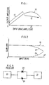
- FIG. 1 illustrates the typical case.
- the amplitude transfer characteristic of a typical velocity-modulated amplifier consists of a linear portion 10 followed at high drive levels by a smoothly saturating portion 12, reaching a peak output at the "saturation" point 14 when the drive is the "saturation drive” 13.
- FIG. 2 this is plotted as a gain curve to illustrate compensation.
- Curve 12 ⁇ is the tube's gain in dB vs. drive amplitude. If the tube were preceded by a circuit with gain response as shown by curve 16, an amplitude expansion with increasing signal, the resulting over-all response would be greatly linearized, approaching the straight line 18.
- FIG. 3 An early scheme for doing this is shown in FIG. 3.
- a back-to-back pair of diodes such as semiconductor Schottky diodes 22, 24 which have a conductance increasing with signal amplitude.
- diodes such as semiconductor Schottky diodes 22, 24 which have a conductance increasing with signal amplitude.
- This scheme has many weaknesses.
- the characteristics of the diodes do not match the TWT's very well. Also, different TWT's have different saturation characteristics, and it is not feasible to find diodes with all the desired characteristics.
- An object of the invention is to provide a traveling-wave-tube power amplifier having linear amplitude response up to a drive level approaching saturation.
- a further object is to provide an amplifier with constant phase response.
- a further object is to provide an amplifier with reduced harmonic and intermodulation distortion.
- a still further object is to provide an amplifier of increased efficiency and power.
- the linearizer circuit is adjustable to fit a wide variety of amplifier tubes.
- the invention can best be understood by dividing it into two sections, although the performance in combination is the important result.
- FIG. 4 we see a simplified schematic circuit of the basically amplitude-linearizing section.
- this section is in series with the phase linearizer, to be described below, which latter also corrects a small phase distortion introduced by the amplitude section.
- Both sections are in series with the input signal to the amplifier.
- the amplitude predistorter or corrector section has an input terminal 26 and output terminal 28. Between them are connected two pairs of semiconductor diodes such as Schottky diodes 30 and 32, the diodes of each pair being of like polarity and opposite to the diodes of the other pair. Thus the D.C. rectified current merely circulates and the overall impedance is non-directional. This much of the circuit resembles the prior-art circuit of FIG.3. Additional components make the circuit adjustable to provide the desired characteristics to match particular amplifier tubes. A resistor 34 is connected in parallel with the diode pairs to provide an unvarying component of conduction. Individual adjustment is provided by connecting an additional diode 36 and 44 between the junction 38, 48 of the diodes of each pair and rf ground 40.
- a resistor 34 is connected in parallel with the diode pairs to provide an unvarying component of conduction. Individual adjustment is provided by connecting an additional diode 36 and 44 between the junction 38, 48 of the diodes of each pair and rf ground 40.
- D.C. bias currents are fed into the junctions 38, 48. They control the rf levels at which the various diodes become lower impedances and hence expand the transfer characteristic as desired.
- Each D.C. bias is fed through a series inductor 52 bypassed to ground by a capacitor 54, and fed through a resistor 56 connected to an adjustable bias voltage source 58.
- an additional diode 33 may be added in series with one pair 32.
- the diodes preferably comprise a combination of low, medium and high-barrier Schottky diodes in order to better approximate certain distortion characteristics.
- resistors 62 may be placed in series with one or both pairs.
- a buffer amplifier 60 may be used to isolate the circuit section.
- the amplitude predistorting section in combination with any amplitude effects introduced by the phase section and the inherent distortion of the TWT is discussed below.
- the amplitude section also introduces non-linear phase distortion, due to diose capacitance and lead inductance, which combines with the other non-linear phase characteristics.
- FIG. 5 is shown a set of amplitude-expansion characteristics obtained with the circuit of FIG. 4 with various settings of bias currents I + and I - , illustrating the range of control available with just two external D.C. controls.
- FIG. 6 is a schematic diagram of the phase predistortion section of the linearizer.
- the phase corrector section is thus to introduce a phase advance with increasing drive power.
- FIG. 6 includes pairs of back-to-front diodes similar to the amplitude expander circuit of FIG. 4. Similar components in FIG. 6 are numbered like the corresponding ones in FIG. 4.
- a phase-delay network between input 26 ⁇ and output 28 ⁇ consisting of replacing resistor 34 with a pair of series resistors 60, 62 shunted at their mid-connection to ground 40 ⁇ by a capacitor 64.
- a conventional matching transformer 25 between the incoming RF driver signal and circuit input 26 ⁇ .
- the matching transformer reduces the impedance accordingly; it can for example be a quarter wave matching transformer. It should also be noted that the matching transformer can help to alleviate source loading effects on the phase predistortion section. Because of this benefit, it will be preferable to utilize such a matching transformer also in the input of the amplitude predistortion section. In this way optimal performance is facilitated since source loading effects are minimized.
- the diode pairs 30 ⁇ and 32 ⁇ become lower impedance, reducing the current through the R-C network 60, 62, 64 and thus reducing its inherent phase delay. Also, the series capacitances of diodes 30 ⁇ , 32 ⁇ become more effective in providing phase-advanced current.
- the amount of predistortion is controlled by the bias currents fed into auxiliary diodes 36 ⁇ and 38 ⁇ . Also analogously with the amplitude predistortion section, the diodes of this section preferably comprise both low and medium barrier Schottky diodes, to better approximate desired distortion characteristics.
- phase predistortion section The positioning of matching transformer 25 ahead of the phase predistortion section of course assumes that the input signal is first to be directed through the phase predistortion section, rather than the amplitude predistortion section. This is in fact the preferred arrangement; however, an arrangement in which the amplitude predistortion section is positioned first may also be possible.
- control of the predistortion is provided by the D.C. bias currents.
- the predistortion will in both cases depend also on the amplitude level of the input signal, due to the nature of these diode circuits. If the level of input drive into both sections is not above a certain range, they will not be operating within the appropriate transfer region which would provide a proper predistortion function. Also the optimal degree of predistortion may not be obtainable without controlling the gain level of the input signal. Accordingly, it is preferred to insert a conventional linear gain control circuit (not shown) in series with and ahead of each section. The capability to adjust the input signal drive level thereby provided will make possible optimal adjustability of the predistortion and these provide optimal compatability between the successive stages.
- a further conventional linear gain control circuit which may preferably be utilized in series between the output of the linearizer and the TWT amplifier sought to be driven are a further conventional linear gain control circuit, and a conventional amplitude equalizer.
- the utility for this linear gain control occurs when the output of the linearizer is within a range which is either too high or too low for a particular TWT.
- the range of the drive signal must not be so great as to drive the TWT into saturation, nor so low that only a fraction of the expected power output is produced.
- a final linear gain control may be useful where it is necessary to match the dynamic range of the linearizer output to the input requirements of a TWT which may demand a somewhat different range.
- the signal from the linearizer may also not have the degree of flatness of response over a desired frequency range for a given communications application.
- the network may not have the same response to a given signal level at one frequency as compared to another frequency in the desired range.
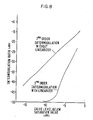
- FIG. 7 is a graph of relative phase delay of the uncompensated TWT amplifier 70 and the integrated amplifier 72 as linearized with the inventive circuit.
- FIG. 8 is a graph of the intermodulation ratio of the dominant third order intermodulation product of an uncompensated TWT amplifier 74 and the linearized integrated amplifier 76. Higher order odd intermodulation ratios are well below the third order.
Abstract
Description
- The invention pertains to microwave amplifiers using linear-beam electron tubes such as traveling-wave tubes or klystrons as the power output generators. These tubes have transfer characteristics which saturate with increasing rf drive levels. When amplifying amplitude-modulated signals such as television the modulation level must be limited to the linear part of the characteristic to preserve amplitude linearity and low harmonic and intermodulation distortion. (In satellite transmission systems several channels are often transmitted by the same tube. Thus the high efficiencies obtained by driving near saturation are not obtainable.)
- It is known that the distortions incurred in driving the output tube near saturation can be lessened by predistorting their input signals in amplitude and phase response to the inverse of the tube's transfer characteristic, so the overall response approaches linearity.
- FIG. 1 illustrates the typical case. The amplitude transfer characteristic of a typical velocity-modulated amplifier consists of a
linear portion 10 followed at high drive levels by a smoothly saturatingportion 12, reaching a peak output at the "saturation"point 14 when the drive is the "saturation drive" 13. In FIG. 2 this is plotted as a gain curve to illustrate compensation. Curve 12ʹ is the tube's gain in dB vs. drive amplitude. If the tube were preceded by a circuit with gain response as shown bycurve 16, an amplitude expansion with increasing signal, the resulting over-all response would be greatly linearized, approaching thestraight line 18. - An early scheme for doing this is shown in FIG. 3. In series with the input signal line are inserted a back-to-back pair of diodes, such as
semiconductor Schottky diodes - This scheme has many weaknesses. The characteristics of the diodes do not match the TWT's very well. Also, different TWT's have different saturation characteristics, and it is not feasible to find diodes with all the desired characteristics.
- An object of the invention is to provide a traveling-wave-tube power amplifier having linear amplitude response up to a drive level approaching saturation.
- A further object is to provide an amplifier with constant phase response.
- A further object is to provide an amplifier with reduced harmonic and intermodulation distortion.
- A still further object is to provide an amplifier of increased efficiency and power.
- These objects are realized by a circuit for predistortion to cancel the distortion produced in the velocity-modulated output tube. The linearizer circuit is adjustable to fit a wide variety of amplifier tubes.
-
- FIG. 1 is a sketch of the amplitude transfer characteristic of a typical traveling-wave tube.
- FIG. 2 is a sketch of the transfer characteristic of FIG. 1 plotted on a scale of decibel gains.
- FIG. 3 is a schematic diagram of a prior-art compensating circuit.
- FIG. 4 is a schematic diagram of a circuit embodying the amplitude section of the invention.
- FIG. 5 is a set of typical amplitude-expansion characteristics.
- FIG. 6 is a schematic diagram of a circuit embodying the phase section of the invention.
- FIG. 7 is a graph of the uncorrected and corrected phase response of a typical amplifier.
- FIG. 8 is a graph of the intermodulation distortion of a typical amplifier.
- The invention can best be understood by dividing it into two sections, although the performance in combination is the important result.
- In FIG. 4 we see a simplified schematic circuit of the basically amplitude-linearizing section. In operation this section is in series with the phase linearizer, to be described below, which latter also corrects a small phase distortion introduced by the amplitude section. Both sections are in series with the input signal to the amplifier.
- The amplitude predistorter or corrector section has an
input terminal 26 andoutput terminal 28. Between them are connected two pairs of semiconductor diodes such as Schottkydiodes resistor 34 is connected in parallel with the diode pairs to provide an unvarying component of conduction. Individual adjustment is provided by connecting anadditional diode junction rf ground 40. D.C. bias currents are fed into thejunctions series inductor 52 bypassed to ground by acapacitor 54, and fed through aresistor 56 connected to an adjustablebias voltage source 58. - For certain distortion characteristics an
additional diode 33 may be added in series with onepair 32. The diodes preferably comprise a combination of low, medium and high-barrier Schottky diodes in order to better approximate certain distortion characteristics. Alsoresistors 62 may be placed in series with one or both pairs. Abuffer amplifier 60 may be used to isolate the circuit section. - The performance of the amplitude predistorting section, in combination with any amplitude effects introduced by the phase section and the inherent distortion of the TWT is discussed below. Of course the amplitude section also introduces non-linear phase distortion, due to diose capacitance and lead inductance, which combines with the other non-linear phase characteristics.
- In FIG. 5 is shown a set of amplitude-expansion characteristics obtained with the circuit of FIG. 4 with various settings of bias currents I+ and I-, illustrating the range of control available with just two external D.C. controls.
- FIG. 6 is a schematic diagram of the phase predistortion section of the linearizer. In the TWT amplifier tube, there is a phase lag that sets in at drive levels approaching saturation and increases with increasing drive. This is due to the inherent non-linearity of the velocity modulation process for large signals and the slowing down of the electrons as energy is extracted from them into the interaction circuit. The purpose of the phase corrector section is thus to introduce a phase advance with increasing drive power.
- The circuit to do this, FIG. 6, includes pairs of back-to-front diodes similar to the amplitude expander circuit of FIG. 4. Similar components in FIG. 6 are numbered like the corresponding ones in FIG. 4. In addition there is a phase-delay network between input 26ʹ and output 28ʹ consisting of replacing
resistor 34 with a pair ofseries resistors capacitor 64. Also preferably added is aconventional matching transformer 25 between the incoming RF driver signal and circuit input 26ʹ. If as is typical, the impedance of the input signal source is the 50-ohm standard impedance of typical microwave networks, and the phase predistortion section would like to see a lower impedance, for example 25 ohms, then the matching transformer reduces the impedance accordingly; it can for example be a quarter wave matching transformer. It should also be noted that the matching transformer can help to alleviate source loading effects on the phase predistortion section. Because of this benefit, it will be preferable to utilize such a matching transformer also in the input of the amplitude predistortion section. In this way optimal performance is facilitated since source loading effects are minimized. - As the signal rises the diode pairs 30ʹ and 32ʹ become lower impedance, reducing the current through the
R-C network - It will be recalled in the case of the amplitude predistortion section, that the curves illustrated in FIG. 5, plotting loss in dB with input power, showed some of the various amplitude expansion characteristics possible with various settings of D.C. bias. These curves are also generally illustrative of some of the phase expansion characteristics obtainabler from the phase predistortion section at various settings of D.C. bias. Utilizing the vertical left hand axis, it will be seen that these curves may also be considered plots of phase shift in degrees with input power. Just as in the case of the amplitude predistortion section, a good range of adjustability for various desired predistortion characteristics is therefore obtainable.
- The positioning of matching
transformer 25 ahead of the phase predistortion section of course assumes that the input signal is first to be directed through the phase predistortion section, rather than the amplitude predistortion section. This is in fact the preferred arrangement; however, an arrangement in which the amplitude predistortion section is positioned first may also be possible. - In both the amplitude and phase predistortion sections, it has been stated above that control of the predistortion is provided by the D.C. bias currents. However, the predistortion will in both cases depend also on the amplitude level of the input signal, due to the nature of these diode circuits. If the level of input drive into both sections is not above a certain range, they will not be operating within the appropriate transfer region which would provide a proper predistortion function. Also the optimal degree of predistortion may not be obtainable without controlling the gain level of the input signal. Accordingly, it is preferred to insert a conventional linear gain control circuit (not shown) in series with and ahead of each section. The capability to adjust the input signal drive level thereby provided will make possible optimal adjustability of the predistortion and these provide optimal compatability between the successive stages.
- Other components which may preferably be utilized in series between the output of the linearizer and the TWT amplifier sought to be driven are a further conventional linear gain control circuit, and a conventional amplitude equalizer. The utility for this linear gain control occurs when the output of the linearizer is within a range which is either too high or too low for a particular TWT. As is well-known, the range of the drive signal must not be so great as to drive the TWT into saturation, nor so low that only a fraction of the expected power output is produced. Thus a final linear gain control may be useful where it is necessary to match the dynamic range of the linearizer output to the input requirements of a TWT which may demand a somewhat different range.
- The signal from the linearizer, adjusted as above, may also not have the degree of flatness of response over a desired frequency range for a given communications application. In particular, the network may not have the same response to a given signal level at one frequency as compared to another frequency in the desired range. Thus depending on the application, it can be desirable to add a conventional amplitude equalizer to compensate this response between the linearizer output and the TWT input to achieve a desired reasonable degree of flatness of frequency response.
- FIG. 7 is a graph of relative phase delay of the
uncompensated TWT amplifier 70 and theintegrated amplifier 72 as linearized with the inventive circuit. - An important net effect on the performance degradation from the combined amplitude and phase non-linearity of the TWT is the resultant intermodulation distortion. This is most important during simultaneous transmission of several signal channels as is usual with satellite communication networks. FIG. 8 is a graph of the intermodulation ratio of the dominant third order intermodulation product of an uncompensated TWT amplifier 74 and the linearized integrated amplifier 76. Higher order odd intermodulation ratios are well below the third order.
- The above particular embodiments are examplary. It will be obvious to those skilled in the art that many variations may be substituted within the scope of the invention, as different types of diodes such as PIN diodes, etc. Many kinds of circuit wiring may be used, with discrete at integrated circuits.
- The scope of the invention is to be limited only by the following claims and their legal equivalents.
Claims (4)
an amplitude compensating section and a phase compensating section, in series, each of said compensating sections comprising:
an input terminal and an output terminal,
a first pair of semiconductor diodes connected in series in the same, first direction of polarization between said input and output terminals,
a second pair of semiconductor diodes connected in series in the same, second direction opposite to said first direction between said input and output terminals,
A resistor connected between said input and output terminals,
a fifth semiconductor diode connected from the first common connection between said first pair of diodes and a radio-frequency ground,
means for supplying an adjustable forward bias current through said fifth diode,
a sixth semiconductor diode connected in a polarity opposite to said fifth diode from a second common connection between said second pair of diodes and said radio-frequency ground, means for supplying an independently adjustable forward bias current through said sixth diode,
said phase compensating section also comprising a capacitor connected between a midpoint of said resistor and said ground.
Applications Claiming Priority (2)
| Application Number | Priority Date | Filing Date | Title |
|---|---|---|---|
| US912448 | 1986-09-26 | ||
| US06/912,448 US4752743A (en) | 1986-09-26 | 1986-09-26 | Linearizer for TWT amplifiers |
Publications (3)
| Publication Number | Publication Date |
|---|---|
| EP0261813A2 true EP0261813A2 (en) | 1988-03-30 |
| EP0261813A3 EP0261813A3 (en) | 1989-02-22 |
| EP0261813B1 EP0261813B1 (en) | 1992-04-15 |
Family
ID=25431940
Family Applications (1)
| Application Number | Title | Priority Date | Filing Date |
|---|---|---|---|
| EP87307604A Expired - Lifetime EP0261813B1 (en) | 1986-09-26 | 1987-08-27 | Linearizer for twt amplifiers |
Country Status (4)
| Country | Link |
|---|---|
| US (1) | US4752743A (en) |
| EP (1) | EP0261813B1 (en) |
| JP (1) | JP2529114B2 (en) |
| DE (1) | DE3778271D1 (en) |
Cited By (4)
| Publication number | Priority date | Publication date | Assignee | Title |
|---|---|---|---|---|
| EP0620661A1 (en) * | 1993-04-14 | 1994-10-19 | Sumitomo Electric Industries, Limited | Distortion generating circuit |
| US5452389A (en) * | 1993-04-16 | 1995-09-19 | Sumitomo Electric Industries, Ltd. | Semiconductor element module |
| EP1871005A1 (en) * | 2006-06-21 | 2007-12-26 | Emcore Corporation | In-line distortion cancellation circuits for linearization of electronic and optical signals with phase and frequency adjustment |
| CN101127534B (en) * | 2007-08-14 | 2010-05-26 | 锐德科无线通信技术(上海)有限公司 | Simulated pre-distortion circuit and method |
Families Citing this family (19)
| Publication number | Priority date | Publication date | Assignee | Title |
|---|---|---|---|---|
| US5210633A (en) * | 1990-09-12 | 1993-05-11 | General Instrument Corporation | Apparatus and method for linearizing the operation of an external optical modulator |
| US5172068A (en) * | 1990-09-17 | 1992-12-15 | Amoco Corporation | Third-order predistortion linearization circuit |
| US5394113A (en) * | 1992-08-28 | 1995-02-28 | Harris Corporation | High impedance low-distortion linear amplifier |
| US5523716A (en) * | 1994-10-13 | 1996-06-04 | Hughes Aircraft Company | Microwave predistortion linearizer |
| US5838195A (en) * | 1996-08-06 | 1998-11-17 | Northrop Grumman Corporation | Reduction of second order harmonic distortion in high power TWT amplifiers |
| US5789978A (en) * | 1996-11-25 | 1998-08-04 | Space Systems/Loral, Inc. | Ku-band linearizer bridge |
| FI103743B (en) * | 1997-08-27 | 1999-08-31 | Insinoeoeritoimisto Juhana Yli | predistortion linearizer |
| US6204718B1 (en) * | 1999-06-25 | 2001-03-20 | Scientific-Atlanta, Inc. | Method and apparatus for generating second-order predistortion without third-order distortion |
| US6255908B1 (en) | 1999-09-03 | 2001-07-03 | Amplix | Temperature compensated and digitally controlled amplitude and phase channel amplifier linearizer for multi-carrier amplification systems |
| US6188279B1 (en) * | 1999-11-03 | 2001-02-13 | Space Systems/Loral, Inc. | Low cost miniature broadband linearizer |
| US7242725B2 (en) * | 2003-04-02 | 2007-07-10 | Harris Stratex Networks Operating Corporation | Adaptive broadband post-distortion receiver for digital radio communication system |
| JP4546052B2 (en) * | 2003-07-24 | 2010-09-15 | 日本電気株式会社 | AM-PM distortion compensation circuit and method |
| JP4739717B2 (en) * | 2004-09-21 | 2011-08-03 | 古野電気株式会社 | Distortion compensation circuit |
| JP4319681B2 (en) * | 2004-10-28 | 2009-08-26 | 三菱電機株式会社 | Linearizer |
| US7596326B2 (en) * | 2005-10-27 | 2009-09-29 | Emcore Corporation | Distortion cancellation circuitry for optical receivers |
| US7508266B1 (en) | 2006-08-29 | 2009-03-24 | Pmc-Sierra, Inc. | Method for enhancing linearity of a transistor amplifier using switched capacitive loads |
| CN103580658B (en) * | 2013-11-07 | 2016-06-29 | 中国电子科技集团公司第四十一研究所 | A kind of radio-frequency switch circuit |
| US9625515B2 (en) | 2014-06-09 | 2017-04-18 | Communications & Power Industries Llc | Predicting the end of service life for a vacuum electron device |
| CN113285679B (en) * | 2021-04-23 | 2022-08-23 | 中国电子科技集团公司第二十九研究所 | Ultra-wideband miniaturized amplitude expanding circuit |
Citations (4)
| Publication number | Priority date | Publication date | Assignee | Title |
|---|---|---|---|---|
| US3210680A (en) * | 1962-12-24 | 1965-10-05 | Collins Radio Co | Audio signal variable attentuating circuit |
| US3675138A (en) * | 1970-09-23 | 1972-07-04 | Communications Satellite Corp | Reduction of intermodulation products |
| DE2140851A1 (en) * | 1971-08-14 | 1973-02-15 | Rohde & Schwarz | PRE-DISTORTION CIRCUIT FOR NONLINEAR AMPLIFIER |
| GB1419519A (en) * | 1972-10-02 | 1975-12-31 | Pye Ltd | Correcting amplifier non-linearity |
Family Cites Families (1)
| Publication number | Priority date | Publication date | Assignee | Title |
|---|---|---|---|---|
| FR2204334A5 (en) * | 1972-10-20 | 1974-05-17 | Thomson Csf |
-
1986
- 1986-09-26 US US06/912,448 patent/US4752743A/en not_active Expired - Fee Related
-
1987
- 1987-08-27 EP EP87307604A patent/EP0261813B1/en not_active Expired - Lifetime
- 1987-08-27 DE DE8787307604T patent/DE3778271D1/en not_active Expired - Fee Related
- 1987-09-10 JP JP62225447A patent/JP2529114B2/en not_active Expired - Lifetime
Patent Citations (4)
| Publication number | Priority date | Publication date | Assignee | Title |
|---|---|---|---|---|
| US3210680A (en) * | 1962-12-24 | 1965-10-05 | Collins Radio Co | Audio signal variable attentuating circuit |
| US3675138A (en) * | 1970-09-23 | 1972-07-04 | Communications Satellite Corp | Reduction of intermodulation products |
| DE2140851A1 (en) * | 1971-08-14 | 1973-02-15 | Rohde & Schwarz | PRE-DISTORTION CIRCUIT FOR NONLINEAR AMPLIFIER |
| GB1419519A (en) * | 1972-10-02 | 1975-12-31 | Pye Ltd | Correcting amplifier non-linearity |
Cited By (5)
| Publication number | Priority date | Publication date | Assignee | Title |
|---|---|---|---|---|
| EP0620661A1 (en) * | 1993-04-14 | 1994-10-19 | Sumitomo Electric Industries, Limited | Distortion generating circuit |
| US5600472A (en) * | 1993-04-14 | 1997-02-04 | Sumitomo Electric Industries, Ltd. | Distortion generating circuit |
| US5452389A (en) * | 1993-04-16 | 1995-09-19 | Sumitomo Electric Industries, Ltd. | Semiconductor element module |
| EP1871005A1 (en) * | 2006-06-21 | 2007-12-26 | Emcore Corporation | In-line distortion cancellation circuits for linearization of electronic and optical signals with phase and frequency adjustment |
| CN101127534B (en) * | 2007-08-14 | 2010-05-26 | 锐德科无线通信技术(上海)有限公司 | Simulated pre-distortion circuit and method |
Also Published As
| Publication number | Publication date |
|---|---|
| DE3778271D1 (en) | 1992-05-21 |
| EP0261813A3 (en) | 1989-02-22 |
| EP0261813B1 (en) | 1992-04-15 |
| JP2529114B2 (en) | 1996-08-28 |
| JPS6386603A (en) | 1988-04-18 |
| US4752743A (en) | 1988-06-21 |
Similar Documents
| Publication | Publication Date | Title |
|---|---|---|
| EP0261813B1 (en) | Linearizer for twt amplifiers | |
| US6538509B2 (en) | Linearizer for a power amplifier | |
| US5606286A (en) | Predistortion linearization | |
| KR100887116B1 (en) | Class e doherty amplifier topology for high efficiency signal transmitters | |
| CA2616285C (en) | Predistortion linearization device with adjustable amplitude and shape | |
| US3755754A (en) | Predistortion compensation for a microwave amplifier | |
| US4068186A (en) | Circuit for compensating for nonlinear characteristics in high-frequency amplifiers | |
| US7288987B2 (en) | RF amplifier employing active load linearization | |
| US4554514A (en) | Predistortion circuit with feedback | |
| US4465980A (en) | Predistortion circuit for a power amplifier | |
| US5966049A (en) | Broadband linearizer for power amplifiers | |
| US4588958A (en) | Adjustable reflective predistortion circuit | |
| US4453133A (en) | Active predistorter for linearity compensation | |
| US5576660A (en) | Broadband predistortion linearizer with automatic temperature compensation for microwave amplifiers | |
| EP0603687B1 (en) | Gain linearization with coplanar waveguide | |
| GB2229057A (en) | Drive network for multichannel amplifiers | |
| JPH03195101A (en) | Feed-forward predistortion linearizer | |
| US4532477A (en) | Distortion compensation for a microwave amplifier | |
| JP2002076781A (en) | High frequency amplifier, feed forward amplifier and distortion compensated amplifier | |
| US6188279B1 (en) | Low cost miniature broadband linearizer | |
| JP3335907B2 (en) | Distortion compensation circuit and low distortion semiconductor amplifier | |
| US4733194A (en) | Apparatus and method for paralleling power field effect transistors in high frequency amplifiers | |
| US4119923A (en) | Distortion corrector for wide-band transistorized amplification stages | |
| CN113630092B (en) | Reflection type adjustable predistorter | |
| Katz et al. | The evolution of linearizers for high power amplifiers |
Legal Events
| Date | Code | Title | Description |
|---|---|---|---|
| PUAI | Public reference made under article 153(3) epc to a published international application that has entered the european phase |
Free format text: ORIGINAL CODE: 0009012 |
|
| AK | Designated contracting states |
Kind code of ref document: A2 Designated state(s): DE FR GB |
|
| PUAL | Search report despatched |
Free format text: ORIGINAL CODE: 0009013 |
|
| AK | Designated contracting states |
Kind code of ref document: A3 Designated state(s): DE FR GB |
|
| 17P | Request for examination filed |
Effective date: 19890710 |
|
| 17Q | First examination report despatched |
Effective date: 19910709 |
|
| GRAA | (expected) grant |
Free format text: ORIGINAL CODE: 0009210 |
|
| AK | Designated contracting states |
Kind code of ref document: B1 Designated state(s): DE FR GB |
|
| REF | Corresponds to: |
Ref document number: 3778271 Country of ref document: DE Date of ref document: 19920521 |
|
| ET | Fr: translation filed | ||
| PLBE | No opposition filed within time limit |
Free format text: ORIGINAL CODE: 0009261 |
|
| STAA | Information on the status of an ep patent application or granted ep patent |
Free format text: STATUS: NO OPPOSITION FILED WITHIN TIME LIMIT |
|
| 26N | No opposition filed | ||
| PGFP | Annual fee paid to national office [announced via postgrant information from national office to epo] |
Ref country code: FR Payment date: 19980619 Year of fee payment: 12 |
|
| PGFP | Annual fee paid to national office [announced via postgrant information from national office to epo] |
Ref country code: GB Payment date: 19980624 Year of fee payment: 12 |
|
| PGFP | Annual fee paid to national office [announced via postgrant information from national office to epo] |
Ref country code: DE Payment date: 19980930 Year of fee payment: 12 |
|
| PG25 | Lapsed in a contracting state [announced via postgrant information from national office to epo] |
Ref country code: GB Free format text: LAPSE BECAUSE OF NON-PAYMENT OF DUE FEES Effective date: 19990827 |
|
| GBPC | Gb: european patent ceased through non-payment of renewal fee |
Effective date: 19990827 |
|
| PG25 | Lapsed in a contracting state [announced via postgrant information from national office to epo] |
Ref country code: FR Free format text: LAPSE BECAUSE OF NON-PAYMENT OF DUE FEES Effective date: 20000428 |
|
| PG25 | Lapsed in a contracting state [announced via postgrant information from national office to epo] |
Ref country code: DE Free format text: LAPSE BECAUSE OF NON-PAYMENT OF DUE FEES Effective date: 20000601 |
|
| REG | Reference to a national code |
Ref country code: FR Ref legal event code: ST |