EP0260365A1 - Position and displacement sensor, particularly for the position and displacement of a human finger, in particular for realising an attenuator - Google Patents
Position and displacement sensor, particularly for the position and displacement of a human finger, in particular for realising an attenuator Download PDFInfo
- Publication number
- EP0260365A1 EP0260365A1 EP86401840A EP86401840A EP0260365A1 EP 0260365 A1 EP0260365 A1 EP 0260365A1 EP 86401840 A EP86401840 A EP 86401840A EP 86401840 A EP86401840 A EP 86401840A EP 0260365 A1 EP0260365 A1 EP 0260365A1
- Authority
- EP
- European Patent Office
- Prior art keywords
- sensor
- strip
- voltage
- substrate
- output voltage
- Prior art date
- Legal status (The legal status is an assumption and is not a legal conclusion. Google has not performed a legal analysis and makes no representation as to the accuracy of the status listed.)
- Ceased
Links
Images


Classifications
-
- G—PHYSICS
- G01—MEASURING; TESTING
- G01D—MEASURING NOT SPECIALLY ADAPTED FOR A SPECIFIC VARIABLE; ARRANGEMENTS FOR MEASURING TWO OR MORE VARIABLES NOT COVERED IN A SINGLE OTHER SUBCLASS; TARIFF METERING APPARATUS; MEASURING OR TESTING NOT OTHERWISE PROVIDED FOR
- G01D5/00—Mechanical means for transferring the output of a sensing member; Means for converting the output of a sensing member to another variable where the form or nature of the sensing member does not constrain the means for converting; Transducers not specially adapted for a specific variable
- G01D5/12—Mechanical means for transferring the output of a sensing member; Means for converting the output of a sensing member to another variable where the form or nature of the sensing member does not constrain the means for converting; Transducers not specially adapted for a specific variable using electric or magnetic means
- G01D5/14—Mechanical means for transferring the output of a sensing member; Means for converting the output of a sensing member to another variable where the form or nature of the sensing member does not constrain the means for converting; Transducers not specially adapted for a specific variable using electric or magnetic means influencing the magnitude of a current or voltage
- G01D5/16—Mechanical means for transferring the output of a sensing member; Means for converting the output of a sensing member to another variable where the form or nature of the sensing member does not constrain the means for converting; Transducers not specially adapted for a specific variable using electric or magnetic means influencing the magnitude of a current or voltage by varying resistance
- G01D5/165—Mechanical means for transferring the output of a sensing member; Means for converting the output of a sensing member to another variable where the form or nature of the sensing member does not constrain the means for converting; Transducers not specially adapted for a specific variable using electric or magnetic means influencing the magnitude of a current or voltage by varying resistance by relative movement of a point of contact or actuation and a resistive track
Definitions
- the present invention generally relates to position and / or displacement sensors, in particular such sensors capable of producing an attenuator of the potentiometric type.
- It relates more particularly to a sensor for the position and / or displacement of a human finger.
- potentiometers and voltage dividers comprising a fixed electrical resistance and a cursor able to move along this resistance and coming into contact with a variable area of this resistance.
- the subject of the present invention is a sensor comprising such a resistance, in which the cursor is replaced by a human finger, or by another mobile element, capable of pressing, in a determined position of said resistance, an area of a conductive element. substantially parallel to the resistor, so as to make an electrical contact, at the pressure zone, between said resistor and said conductive element.
- the subject of the invention is therefore a position and displacement sensor characterized in that it comprises: a conductive strip established on one face of a first elongated insulating substrate; an elongated resistive strip established on one face of a second elongated insulating substrate, at least one of the two substrates being flexible and these two substrates being arranged opposite one another so that the resistive strip is opposite the conductive strip, a short distance from it; a pair of electrical conductors each having a first end connected to a different end of the resistive strip; and a third electrical conductor having a first end connected to the conductive strip.
- the substrate of the resistive strip is flexible, while the substrate of the conductive strip is rigid.
- the aforementioned sensor can be applied to produce an attenuator in which the reduced potential difference is taken between the second end of the third conductor connected to the conductive strip and the second end of one of the conductors connected to one end of the resistive strip. , with respect to the potential difference, the total potential difference being applied between the second ends of the two conductors connected to the ends of the resistive strip.
- Means can be provided in such a sensor to check the quality of the local contact between the resistive strip and the conductive strip, due to the pressure, at this area, of a finger or other element on the flexible substrate.
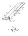
- FIGS. 1 to 3 showing the structure of the sensor according to the invention, as well as to FIGS. 4 and 5 illustrating this sensor in operation.
- the flexible substrate 3 is concave opposite the rigid substrate 1, its concavity being caused for example by the deposition of the conductive plastic on it.
- the two substrates 1 and 3 are joined together along their lateral edges 8 and 9, while they are spaced apart in their elongated middle zone, a space 10 normally existing (as visible in FIG. 2 in particular) between the collector 2 and track 4.
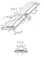
- FIGS. 4 and 5 it can be seen that when pressure is exerted, for example by means of a human finger 11, on the flexible substrate 3, in a determined zone 12 thereof, the track 4 comes into contact, in this zone 12, with the collector 2, as visible in particular in FIG. 5. At the level of zone 12, the track 4 is in mechanical and electrical contact with the collector 2.
- the device of FIGS. 1 to 3 makes it possible to perform a function equivalent to that of a potentiometer, the pressure of the finger filling the role of the cursor of a classic potentiometer.
- rectangle X we find - schematically the resistive track 4 and the conductive collector 2, as well as the electrical conductors 5, 6 and 7 with their respective first ends 5a, 6a and 7a.
- the resistive track 4 can be either linear or functional. Furthermore, it can include intermediate sockets, a midpoint and / or at least one heel resistance (as will be illustrated below) to perform additional functions.
- measurements of the ratiometric type are generally carried out by determining the ratio , by calling VA, V B , V c the potentials at points A, B, C respectively (see FIG. 6), that is to say at the second ends of the conductors 5, 6 and 7 respectively.
- FIG. 6 is shown - schematically by a block Y the processing electronics comprising three inputs connected to points A, B and C and a digital output S.
- FIG. 7 illustrates the part of FIG. 6 included in rectangle X, but by adding a heel resistor 13 connected in series with the resistive track 4; the end 13a of the heel resistor 13 not connected to the resistive track 4 is connected to the first end of a conductor 14.
- the second ends, not connected to the terminals have been noted Ai, Bi, Ci and Di respectively. elements 4, 2 and 13, conductors 14, 5, 7 and 6 respectively.
- One of the problems posed by the sensor according to the invention is the control of the contact between the track 4 and the collector 2 in the zone 12 - in particular the detection of a good contact between these two elements under the effect of an exerted pressure. on track 4, for example using a finger - to eliminate non-significant measurements when the pressure is not clear.
- a curve d is shown showing the variation of the voltage V B 1 (at point Bi in FIG. 7) as a function of time t, when the assembly of FIG. 7 is supplied between the points A 1 and Di, with a voltage U, and when we observe the voltage V B , with respect to V D1 .
- the horizontal line W represents the good contact threshold, V a1 being less than the threshold W in the event of good contact between the track 4 and the collector 2 (zone c), while V B1 is greater than the threshold W in the event of absence of contact (outside zone c, i.e. to the right and left of it).
- the curve d therefore shows what happens when the finger 11 is pressed on track 4 in zone 12, with passage from non-contact to contact (in the zone of good contact c).
- the variation of the voltage V B1 depends of course on the pressure exerted by the finger, on the surface on which the pressure is exerted (therefore on the zone e of the track 4 short-circuited by the collector 4, zone e illustrated on FIG. 6) and also of the voltage U and of the relationship between the value R of the heel resistance 13 and the resistance P of the track 4.
- V B1 The variation of V B1 is given by the formula
- FIGS. 9 and 10 two assemblies have been illustrated making it possible to detect a good frank contact between the track 4 and the collector 2.
- a comparator 15 is used to detect the variation of V B1 with respect to a bias voltage V E defined by a voltage divider with two resistors 16 and 17 of respective values R 1 and R 2 .
- the comparator 15 will output a validation output signal v when V B1 is greater than V e which in fact corresponds to the threshold voltage W defined in FIG. 8 and which is obtained thanks to the voltage divider 16, 17.
- the absence of the validation signal v means that the contact between track 4 and collector 2 does not exist or is not straightforward and that the measurement must be eliminated.
- an analog multiplexer 16b and an analog / digital (or analog / digital) converter 17b are used to measure V S1 -V to check the good contact between the track 4 and the collector 3. D1 and V C1 -V D i.
- the multiplexer 16b multiplexes the voltages V B1 and V C1 , the output of the multiplexer 16b constituting the main input of the converter 17b which receives the voltages V A1 and V D1 as positive and negative reference voltages respectively.
- the digital output is available in Si and it consists, in the event of frank contact between track 4 and collector 2, by a validation signal vi.
- the sensor according to the invention can not only serve as an attenuator, but can provide various information in the case where the finger is replaced by an element movable relative to the sensor, for example the position, the displacement and / or the speed of this element. mobile (or possibly with your finger). It is also possible to perform control functions with the sensor according to the invention.
- This sensor can operate in different ways, namely incrementally, absolutely, parallel, series, synchronously, etc.
- FIGs 11, 12 and 13 there are illustrated three embodiments of a treatment using the sensor according to the invention as - shown diagrammatically in Figures 6 and 7 (without or with heel resistance).
- the assembly of FIG. 9 has been resumed with a comparator 15 for debiting a validation signal v, in the event of good contact;
- the processing unit proper comprises an analog / digital converter 18 receiving V C1 on its main input and V B1 and V D1 on its positive and negative reference inputs respectively.
- the output S 2 of the converter 18 directly represents the position of the contact between the track 4 and the collector 2 when the output of the comparator 15 outputs the validation signal V.
- the output S 2 is absolute in this arrangement.
- FIG. 12 also repeats FIG. 9 with a comparator 15 debiting a validation signal v, in the event of good contact, and it also includes, like FIG. 11, an analog / digital converter 18 with the same inputs as the converter 18 of Figure 11 for connection to Bi, Ci and Di.
- FIG. 12 differs from that of FIG. 11 in that it comprises a lock or memory 19 for recording the preceding digital value s 3 debited by the converter 18 on its output S 2 .
- a control unit 20 controls the converter 18, the lock 19 and a comparator 21 which receives, on the one hand, the previous digital value S 3 of the lock 19 and, on the other hand, the current digital value S4 of the converter 18.
- an AND gate 22 only outputs on its output 23 if it receives the validation signal v from the comparator 15, a control signal from the unit 20 and a non-equality signal from the equality output 21 a of the comparator 21, and this through a NON gate 24 (alternatively the input of the AND gate 22 connected to the output 21 a may be a muting input, which avoids using a separate NOT gate).
- Each comparison between sa and s 3 commanded by the control unit 20 will provide meaning information on the output 21a a and possibly a pulse on the output 23, if there is good contact and if the two values compared S 4 and s 3 are different.
- This is relative, incremental information, which indicates only a change in position of the finger or other mobile element, without any reference of absolute origin.
- FIG. 13 it represents the implementation of a microprocessor 25 connected to them points A 1 , Bi, C 1 , C2 of a sensor according to the invention with track 2 and collector 4, with a heel resistance 13, the voltage + U being applied between point A 1 and point Di, the latter connected to ground.
- the microprocessor can for example be of the ⁇ PD 7816 (or u.PD 7811) type, eight-bit monocircuit, with incorporated analog / digital converter having a digital output S 4 .
- FIG. 14 implements, like FIG. 13, a microprocessor 25a which can also be of the uPD 7811 or u.PD 7816 type.
- This microprocessor comprises a multiplexer 16a and an analog / digital converter 17a of the same type as the multiplexer 16b and the converter 17b of FIG. 10; the connections of the units 16a and 17a are analogous to the connections of the units 16b and 17b in FIG. 10.
- the microprocessor is designed to also include a correction unit 26 connected to the digital output Sa of the converter 17a, the digital output S 5 of the microprocessor 25a being constituted by a digital signal j.
- W threshold (see FIG. 8 and its description) for deciding a good contact for the value read in G (sufficient pressure of a finger or of a mobile element)
- Vp value read previously by the converter 17a on the mumplexed input H of the multiplexer 16a, namely V C1 -V D1
- the senor according to the invention illustrated in Figures 1 to 3 although of a very simple and inexpensive embodiment, can be used in very different arrangements for constituting an attenuator, and in particular an attenuator touch, or to make devices for determining the position, displacement and / or speed of displacement of a movable element relative to the sensor, for example for a robotics application.
Landscapes
- Physics & Mathematics (AREA)
- General Physics & Mathematics (AREA)
- Measurement Of Length, Angles, Or The Like Using Electric Or Magnetic Means (AREA)
Abstract
Description
La présente invention concerne généralement les capteurs de position et/ou de déplacement, en particulier de tels capteurs aptes à réaliser un atténuateur du type potentiométrique.The present invention generally relates to position and / or displacement sensors, in particular such sensors capable of producing an attenuator of the potentiometric type.
Elle concerne plus particulièrement un capteur de la position et/ou du déplacement d'un doigt humain.It relates more particularly to a sensor for the position and / or displacement of a human finger.
La technique connaît des potentiomètres et des diviseurs de tension comportant une résistance électrique fixe et un curseur apte à se déplacer le long de cette résistance et entrant en contact avec une zone variable de cette résistance.The technique knows potentiometers and voltage dividers comprising a fixed electrical resistance and a cursor able to move along this resistance and coming into contact with a variable area of this resistance.
La présente invention a pour objet un capteur comportant une telle résistance, dans lequel le curseur est remplacé par un doigt humain, ou par un autre élément mobile, apte à appuyer, en une position déterminée de ladite résitance, une zone d'un élément conducteur sensiblement parallèle à la résistance, de manière à réaliser un contact électrique, au niveau de la zone de pression, entre ladite résistance et ledit élément conducteur.The subject of the present invention is a sensor comprising such a resistance, in which the cursor is replaced by a human finger, or by another mobile element, capable of pressing, in a determined position of said resistance, an area of a conductive element. substantially parallel to the resistor, so as to make an electrical contact, at the pressure zone, between said resistor and said conductive element.
L'invention a donc pour objet un capteur de position et de déplacement caractérisé en ce qu'il comprend : une bande conductrice établie sur une face d'un premier substrat isolant allongé; une bande résistive allongée établie sur une face d'un second substrat isolant allongé, au moins un des deux substrats étant souple et ces deux substrats étant disposés en regard l'un de l'autre de manière que la bande résistive se trouve en face de la bande conductrice, à une faible distance de celle-ci; une paire de conducteurs électriques ayant chacun une première extrémité connectée à une extrémité différente de la bande résistive; et un troisième conducteur électrique ayant une première extrémité connectée à la bande conductrice.The subject of the invention is therefore a position and displacement sensor characterized in that it comprises: a conductive strip established on one face of a first elongated insulating substrate; an elongated resistive strip established on one face of a second elongated insulating substrate, at least one of the two substrates being flexible and these two substrates being arranged opposite one another so that the resistive strip is opposite the conductive strip, a short distance from it; a pair of electrical conductors each having a first end connected to a different end of the resistive strip; and a third electrical conductor having a first end connected to the conductive strip.
De préférence le substrat de la bande résistive est souple, tandis que le substrat de la bande conductrice est rigide.Preferably the substrate of the resistive strip is flexible, while the substrate of the conductive strip is rigid.
En particulier on peut appliquer le capteur précité pour réaliser un atténuateur dans lequel la différence de potentiel réduite est prélevée entre la seconde extrémité du troisième conducteur relié à la bande conductrice et la seconde extrémité d'un des conducteurs relié à une extrémité de la bande résistive, par rapport à la différence de potentiel, la différence de potentiel totale étant appliquée entre les secondes extrémités des deux conducteurs reliés aux extrémités de la bande résistive.In particular, the aforementioned sensor can be applied to produce an attenuator in which the reduced potential difference is taken between the second end of the third conductor connected to the conductive strip and the second end of one of the conductors connected to one end of the resistive strip. , with respect to the potential difference, the total potential difference being applied between the second ends of the two conductors connected to the ends of the resistive strip.
On peut prévoir, dans un tel capteur, des moyens pour vérifier la qualité du contact local entre la bande résistive et la bande conductrice , du fait de la pression, au niveau de cette zone, d'un doigt ou d'un autre élément sur le substrat souple.Means can be provided in such a sensor to check the quality of the local contact between the resistive strip and the conductive strip, due to the pressure, at this area, of a finger or other element on the flexible substrate.
On peut prévoir par ailleurs, connectés aux secondes extrémités des trois conducteurs, un ensemble électronique contrôlé par le capteur, avec éventuellement des moyens pour vérifier le bon contact local entre la bande résistive et la bande conductrice.One can also provide, connected to the second ends of the three conductors, an electronic assembly controlled by the sensor, possibly with means for checking the good local contact between the resistive strip and the conductive strip.
L'invention pourra, de toute façon, être bien comprise à l'aide du complément de description qui suit, ainsi que des dessins ci-annexés, lesquels complément et dessins sont, bien entendu, donnés surtout à titre d'indication.The invention may, in any case, be well understood with the aid of the additional description which follows, as well as of the appended drawings, which supplement and drawings are, of course, given mainly by way of indication.
- La figure 1 représente en perspective un capteur doté des perfectionnements selon l'invention.Figure 1 shows in perspective a sensor with improvements according to the invention.
- La figure 2 est une coupe par II-II de la figure 1.Figure 2 is a section through II-II of Figure 1.
- La figure 3 est une vue éclatée du capteur de la figure 1.Figure 3 is an exploded view of the sensor of Figure 1.
- La figure 4 représente le capteur de la figure 1 en fonctionnement, un doigt assurant un contact entre une zone de la bande résistive avec la bande conductrice.4 shows the sensor of Figure 1 in operation, a finger ensuring contact between an area of the resistive strip with the conductive strip.
- La figure 5 est une coupe par V-V de la figure 4.Figure 5 is a section through V-V of Figure 4.
- La figure 6 illustre, schématiquement, l'analogie d'un capteur selon l'invention avec un potentiomètre classique, ainsi que l'électronique d'utilisation du capteur.FIG. 6 schematically illustrates the analogy of a sensor according to the invention with a conventional potentiometer, as well as the electronics for using the sensor.
- La figure 7 représente un mode d'utilisation du capteur selon l'invention avec une résistance talon.FIG. 7 represents a mode of use of the sensor according to the invention with a heel resistance.
- La figure 8 montre la variation , en fonction du temps, de la tension de sortie d'un tel capteur en l'absence de contact et en cas de contact.FIG. 8 shows the variation, as a function of time, of the output voltage of such a sensor in the absence of contact and in the event of contact.
- Les figures 9 et 10 illustrent deux modes de réalisation d'un montage destiné à vérifier l'existence d'un bon contact entre une zone de la bande résistive et la bande conductrice.Figures 9 and 10 illustrate two embodiments of an assembly intended to verify the existence of a good contact between an area of the resistive strip and the conductive strip.
- Les figures 11, 12 et 13 illustrent trois modes de réalisation de schémas électroniques d'utilisation du capteur des figures 1 à 3 doté d'une résistance talon.Figures 11, 12 and 13 illustrate three embodiments of electronic diagrams of use of the sensor of Figures 1 to 3 with a heel resistance.
- La figure 14 illustre un autre mode de réalisation de l'ensemble électronique d'utilisation d'un tel capteur avec une résistance talon.FIG. 14 illustrates another embodiment of the electronic assembly for using such a sensor with a heel resistance.
- La figure 15, enfin, représente l'organigramme de la mise en oeuvre du montage de la figure 14.FIG. 15, finally, represents the flowchart of the implementation of the assembly of FIG. 14.
Selon l'invention et plus spécialement selon celui de ses modes d'application, ainsi que selon ceux des modes de réalisation de ses diverses parties, auxquels il semble qu'il y ait lieu d'accorder la préférence, se proposant, par exemple, de réaliser un capteur de position et de déplacement, on s'y prend comme suit ou d'une manière analogue.According to the invention and more particularly according to that of its modes of application, as well as according to those of the embodiments of its various parts, to which it seems that there is reason to be given preference, proposing, for example, to make a position and displacement sensor, this is done as follows or in a similar manner.
On se réfère tout d'abord aux figures 1 à 3 montrant la structure du capteur selon l'invention, ainsi qu'aux figures 4 et 5 illustrant ce capteur en fonctionnement.Reference is firstly made to FIGS. 1 to 3 showing the structure of the sensor according to the invention, as well as to FIGS. 4 and 5 illustrating this sensor in operation.
Le capteur selon l'invention comporte :
- -un premier substrat isolant allongé 1, appelé "collecteur", qui est rigide et qui est réalisé par exemple en résine époxy, sur lequel on a déposé une bande ou surface conductrice 2, par exemple en cuivre, revêtu d'un métal noble, tel que l'or, l'argent;
- -un second substrat isolant allongé 3, appelé "piste", qui est souple et qui est réalisé par exemple en "kapton", sur lequel on a déposé une bande ou surface résistive 4, par exemple en une matière plastique conductrice ;
- -une paire de conducteurs électriques 5, 6, dont les
premières extrémités piste 4; et - -un troisième conducteur électrique 7, dont une
première extrémité 7a est connectée aucollecteur 2.
- a first elongated
insulating substrate 1, called a "collector", which is rigid and which is made for example of epoxy resin, on which a conductive strip orsurface 2, for example of copper, coated with a noble metal, has been deposited, such as gold, silver; - a second elongated
insulating substrate 3, called "track", which is flexible and which is produced for example from "kapton", on which a resistive strip orsurface 4 has been deposited, for example from a conductive plastic material; - a pair of
electrical conductors first ends track 4; and - a third
electrical conductor 7, afirst end 7a of which is connected to thecollector 2.
Le substrat souple 3 est concave en regard du substrat rigide 1, sa concavité étant provoquée par exemple par le dépôt de la matière plastique conductrice sur lui.The
Les deux substrats 1 et 3 sont solidarisés le long de leurs bords latéraux 8 et 9, alors qu'ils sont écartés à distance dans leur zone médiane allongée, un espace 10 existant normalement (comme visible sur la figure 2 en particulier) entre le collecteur 2 et la piste 4.The two
En se référant maintenant plus particulièrement aux figures 4 et 5, on voit que lorsqu'on exerce une pression, par exemple au moyen d'un doigt humain 11, sur le substrat souple 3, en une zone déterminée 12 de celui-ci, la piste 4 vient au contact, dans cette zone 12, du collecteur 2, comme visible en particulier sur la figure 5. Au niveau de la zone 12 la piste 4 est en contact mécanique et électrique avec le collecteur 2.Referring now more particularly to FIGS. 4 and 5, it can be seen that when pressure is exerted, for example by means of a
Comme on le voit sur la partie de gauche de la figure 6 (partie entourée par un rectangle X en traits interrompus), le dispositif des figures 1 à 3 permet de réaliser une fonction équivalente à celle d'un potentiomètre, la pression du doigt remplissant le rôle du curseur d'une potentiomètre classique. Dans le rectangle X on retrouve - schématiquement la piste résistive 4 et le collecteur conducteur 2, ainsi que les conducteurs électriques 5, 6 et 7 avec leurs premières extrémités respectives 5a, 6a et 7a.As can be seen on the left-hand part of FIG. 6 (part surrounded by a rectangle X in broken lines), the device of FIGS. 1 to 3 makes it possible to perform a function equivalent to that of a potentiometer, the pressure of the finger filling the role of the cursor of a classic potentiometer. In rectangle X we find - schematically the
Comme dans un potentiomètre classique, la piste résistive 4 peut être soit linéaire, soit fonctionnelle. Par ailleurs, elle peut comporter des prises intermédiaires, un point milieu et/ou au moins une résistance talon (comme cela sera d'ailleurs illustré ci-après) pour réaliser des fonctions annexes.As in a conventional potentiometer, the
Avec un capteur selon l'invention on effectue généralement des mesures du type ratiométrique en déterminant le rapport
Sur la figure 6 on a représenté - schématiquement par un bloc Y l'électronique de traitement comportant trois entrées connectées aux points A, B et C et une sortie numérique S.In FIG. 6 is shown - schematically by a block Y the processing electronics comprising three inputs connected to points A, B and C and a digital output S.
Sur la figure 7 on a illustré la partie de la figure 6 comprise dans le rectangle X, mais en y ajoutant une résistance talon 13 connectée en série avec la piste résistive 4; l'extrémité 13a de la résistance talon 13 non connectée à la piste résistive 4 est connectée à la première extrémité d'un conducteur 14. Sur la figure 7 on a noté respectivement Ai, Bi, Ci et Di les deuxièmes extrémités, non connectées aux éléments 4, 2 et 13, des conducteurs 14, 5, 7 et 6 respectivement.FIG. 7 illustrates the part of FIG. 6 included in rectangle X, but by adding a
Un des problèmes posés par le capteur selon l'invention est le contrôle du contact entre la piste 4 et le collecteur 2 dans la zone 12 - notamment la détection d'un bon contact entre ces deux éléments sous l'effet d'une pression exercée sur la piste 4, par exemple au moyen d'un doigt - afin d'éliminer les mesures non significatives lorsque la pression n'est pas franche.One of the problems posed by the sensor according to the invention is the control of the contact between the
Sur la figure 8 on a représenté une courbe d montrant la variation de la tension VB1 (au point Bi de la figure 7) en fonction du temps t, lorsqu'on alimente le montage de la figure 7 entre les points A1 et Di, avec une tension U, et lorsqu'on observe la tension VB,par rapport à VD1. La droite horizontale W représente le seuil de bon contact, Va1 étant inférieur au seuil W en cas de bon contact entre la piste 4 et le collecteur 2 (zone c), alors que VB1 est supérieur au seuil W en cas d'absence de contact (en dehors de la zone c, c'est-à-dire à droite et à gauche de celle-ci). La courbe d montre donc ce qui se produit lorsqu'on appuie le doigt 11 sur la piste 4 dans la zone 12, avec passage du non contact au contact (dans la zone de bon contact c).In FIG. 8 a curve d is shown showing the variation of the voltage V B 1 (at point Bi in FIG. 7) as a function of time t, when the assembly of FIG. 7 is supplied between the points A 1 and Di, with a voltage U, and when we observe the voltage V B , with respect to V D1 . The horizontal line W represents the good contact threshold, V a1 being less than the threshold W in the event of good contact between the
La variation de la tension VB1 depend bien sûr de la pression exercée par le doigt, de la surface sur laquelle s'exerce la pression (donc de la zone e de la piste 4 court-circuitée par le collecteur 4, zone e illustrée sur la figure 6) et également de la tension U et de la relation entre la valeur R de la résistance talon 13 et la résistance P de la piste 4.The variation of the voltage V B1 depends of course on the pressure exerted by the finger, on the surface on which the pressure is exerted (therefore on the zone e of the
La variation de V B1 est donnée par la formule
Sur les figures 9 et 10 on a illustré deux montages permettant de détecter un bon contact franc entre la piste 4 et le collecteur 2.In FIGS. 9 and 10 two assemblies have been illustrated making it possible to detect a good frank contact between the
Sur la figure 9 on met en oeuvre un comparateur 15 pour détecter la variation de VB1 par rapport à une tension de polarisation VE définie par un diviseur de tension à deux résistances 16 et 17 de valeurs respectives R1 et R2. Le comparateur 15 débitera un signal de sortie de validation v lorsque VB1 est supérieur à Vequi correspond en fait à la tension de seuil W définie sur la figure 8 et qui est obtenue grâce au diviseur de tension 16, 17. L'absence du signal de validation v signifie que le contact entre la piste 4 et le collecteur 2 n'existe pas ou n'est pas franc et que la mesure doit être éliminée.In FIG. 9, a
Dans le cas de la figure 10, on met en oeuvre, pour vérifier le bon contact entre la piste 4 et le collecteur 3, un multiplexeur analogique 16b et un convertisseur analogique/digital (ou analogique/numérique) 17b pour mesurer VS1 -VD1 et VC1 -VDi. Le multiplexeur 16b multiplexe les tensions VB1 et VC1, la sortie du multiplexeur 16b constituant l'entrée principale du convertisseur 17b qui reçoit les tensions VA1 et VD1 comme tensions de référence positive et négative respectivement. La sortie numérique est disponible en Si et elle est constituée, en cas de contact franc entre la piste 4 et le collecteur 2, par un signal de validation vi.In the case of FIG. 10, an analog multiplexer 16b and an analog / digital (or analog / digital)
Le capteur selon l'invention peut non seulement servir d'atténuateur, mais fournir différentes informations dans le cas où le doigt est remplacé par un élément mobile par rapport au capteur, par exemple la position, le déplacement et/ou la vitesse de cet élément mobile (ou éventuellement du doigt). On peut également réaliser des fonctions de commande avec le capteur selon l'invention.The sensor according to the invention can not only serve as an attenuator, but can provide various information in the case where the finger is replaced by an element movable relative to the sensor, for example the position, the displacement and / or the speed of this element. mobile (or possibly with your finger). It is also possible to perform control functions with the sensor according to the invention.
Ce capteur peut fonctionner de différentes ma nières, à savoir de manière incrémentale, absolue, parallèle, série, synchrone, etc.This sensor can operate in different ways, namely incrementally, absolutely, parallel, series, synchronously, etc.
Sur les figures 11, 12 et 13 on a illustré trois modes de réalisation d'un traitement mettant en oeuvre le capteur selon l'invention tel que - schématisé sur les figures 6 et 7 (sans ou avec résistance talon).In Figures 11, 12 and 13 there are illustrated three embodiments of a treatment using the sensor according to the invention as - shown diagrammatically in Figures 6 and 7 (without or with heel resistance).
Sur la figure 11 on a repris le montage de la figure 9 avec un comparateur 15 pour débiter un signal de validation v, en cas de bon contact; l'unité de traitement proprement dite comprend un convertisseur analogique/digital 18 recevant VC1 sur son entrée principale et VB1 et VD1 sur ses entrées de référence positive et négative respectivement. La sortie S2 du convertisseur 18 représente directement la position du contact entre la piste 4 et le collecteur 2 lorsque la sortie du comparateur 15 débite le signal de validation V. La sortie S2 est absolue dans ce montage.In FIG. 11, the assembly of FIG. 9 has been resumed with a
La figure 12 reprend également la figure 9 avec un comparateur 15 débitant un signal de validation v, en cas de bon contact, et elle comporte également, comme la figure 11, un convertisseur analogique/digital 18 avec les mêmes entrées que le convertisseur 18 de la figure 11 pour la connexion à Bi, Ci et Di.FIG. 12 also repeats FIG. 9 with a
Le montage de la figure 12 se distingue de celui de la figure 11 du fait qu'il comporte un verrou ou mémoire 19 pour enregistrer la valeur numérique précédente s3 débitée par le convertisseur 18 sur sa sortie S2. Une unité de contrôle 20 contrôle le convertisseur 18, le verrou 19 et un comparateur 21 qui reçoit, d'une part, la valeur numérique précédente S3 du verrou 19 et, d'autre part, la valeur numérique actuelle S4 du convertisseur 18. Enfin une porte ET 22 ne débite sur sa sortie 23 que si elle reçoit le signal de validation v du comparateur 15, un signal de contrôle de l'unité 20 et un signal de non égalité à partir de la sortie d'égalité 21 a du comparateur 21, et ceci à travers une porte NON 24 (en variante l'entrée de la porte ET 22 connectée à la sortie 21 a peut être une entrée d'inhibition, ce qui évite d'utiliser une porte NON séparée).The assembly of FIG. 12 differs from that of FIG. 11 in that it comprises a lock or
Finalement sur la sortie 23 on a un signal d'horloge et sur la sortie 21 b du comparateur 21 un signal indiquant le signe de la différence entre s4 et S3.Finally on
Chaque comparaison entre sa et s3 commandée par l'unité de contrôle 20 fournira une information de sens sur la sortie 21a a et éventuellement une impulsion sur la sortie 23, s'il y a bon contact et si les deux valeurs comparées S4 et s3 sont différentes. Il s'agit là d'une information relative, incrémentale, qui indique seulement un changement de position du doigt ou autre élément mobile, sans aucune référence d'origine absolue.Each comparison between sa and s 3 commanded by the
Quant à la figure 13, elle représente la mise en oeuvre d'un microprocesseur 25 connecté eux points A1, Bi, C1, C2 d'un capteur selon l'invention à piste 2 et collecteur 4, avec une résistance talon 13, la tension + U étant appliquée entre le point A1 et le point Di, ce dernier connecté à la masse.As for FIG. 13, it represents the implementation of a
Le microprocesseur peut par exemple être du type µPD 7816 (ou u.PD 7811), monocircuit à huit bits, avec convertisseur analogique/digital incorporé ayant une sortie numérique S4.The microprocessor can for example be of the µPD 7816 (or u.PD 7811) type, eight-bit monocircuit, with incorporated analog / digital converter having a digital output S 4 .
La figure 14 met en oeuvre, comme la figure 13, un microprocesseur 25a qui peut également être du type uPD 7811 ou u.PD 7816. Ce microprocesseur comporte un multiplexeur 16a et un convertisseur analogique/digital 17a du même type que le multiplexeur 16b et le convertisseur 17b de la figure 10; les connexions des unités 16a et 17a sont analogues aux connexions des unités 16b et 17b de la figure 10. Le microprocesseur est prévu pour comporter également une unité de correction 26 connectée à la sortie numérique Sa du convertisseur 17a, la sortie numérique S5 du microprocesseur 25a étant constituée par un signal numérique j.FIG. 14 implements, like FIG. 13, a
On va exposer maintenant, avec référence à la figure 15, le fonctionnement du microprocesseur 25a de la figure 14, en définissant préalablement les symboles utilisés dans l'organigramme représentatif du fonctionnement : g : valeur numérique, fournie par le convertisseur 17a, de la tension présente, à l'instant de la mesure, sur l'entrée muftiplexée G du multiplexeur 16a, à savoir VB1 -VD1 h : valeur numérique, fournie par le convertisseur 17a, de la tension présente, à l'instant de la mesure, sur l'entrée multiplexée H du multiplexeur 16a, à savoir VC1 -VD1 We will now expose, with reference to FIG. 15, the operation of the
W : seuil (voir figure 8 et sa description) de décision d'un bon contact pour la valeur lue en G (pression suffisante d'un doigt ou d'un élément mobile)W: threshold (see FIG. 8 and its description) for deciding a good contact for the value read in G (sufficient pressure of a finger or of a mobile element)
Vp: valeur lue précédemment par le convertisseur 17a sur l'entrée mumplexée H du multiplexeur 16a, à savoir VC1 -VD1 Vp: value read previously by the
F : indicateur permettant de mémoriser l'information "bon contact" (action volontaire du doigt, par exemple), matérialisée par F = 1F: indicator allowing to memorize the information "good contact" (voluntary action of the finger, for example), materialized by F = 1
j : valeur numérique de correction, à savoir écart entre deux mesures successives de h (sur H) en présence de l'information "bon contact" (F = 1), donc valeur représentative du déplacement de la zone de pression du doigt ou de l'élément mobile actionnant le capteur.j: digital correction value, namely the difference between two successive measurements of h (on H) in the presence of the "good contact" information (F = 1), therefore a value representative of the displacement of the finger pressure zone or of the movable element actuating the sensor.
Ces symboles étant définis, on peut se reporter maintenant à l'organigramme de la figure 15 dont les dix opérations peuvent être résumées comme suit :
- Opération 1 : à la mise en route du système (mise sous tension), sans aucune action sur le sous capteur, lire la valeur de g
- Opération 2 : calculer le seuil W pour avoir un bon fonctionnement du système et donc détecter un "bon contact" du collecteur sur la piste; pour cela on retranche une unité à la valeur g que l'on vient de lire W = g - 1; mettre les registres "VP" et "F" à zéro
- Opération 3 : lire la valeur de g
- Opération 4 : comparer la valeur g que l'on vient de lire à la valeur W calculée à la mise en route:
- -si g est plus petit que W, cela veut dire qu'une portion suffisante de piste est court-circuitée et qu'il y a donc présence d'un doigt sur le capteur; on peut donc continuer le cycle ("bon contact")
- Opération 5 : si g est supérieur ou égal à W, il n'y a pas à coup sûr un bon contact; on recommence le cycle en mettant à "0" l'indicateur F, puis en allant à l'opération 3
- Opération 6 : si la condition est remplie, on actionne à "1 " l'indicateur F
- Opération 7 : lire la valeur de g
- Opération 8 : calculer la correction (l'écart de position entre la mesure précédente et l'actuelle) j = g - Vp -remplacer la valeur précédente V p par la nouvelle valeur g |Vp = g
- Opération 9 : tester l'indicateur F -si F = 1, transmettre la correction j -si F = 0, mettre l'indicateur F à 1, puis recommencer l'opération 3
- Opération 10 : transmission de la valeur j du déplacement du contact sur la piste ("correction"), puis recommencer l'opération 3
- Operation 1: when the system is started (power up), without any action on the sub-sensor, read the value of g
- Operation 2: calculate the threshold W to have a good functioning of the system and therefore detect a "good contact" of the collector on the track; for this we subtract a unit from the value g which we have just read W = g - 1; set registers "VP" and "F" to zero
- Operation 3: read the value of g
- Operation 4: compare the value g that we have just read with the value W calculated at start-up:
- -if g is smaller than W, this means that a sufficient portion of the track is short-circuited and that there is therefore a finger on the sensor; we can therefore continue the cycle ("good contact")
- Operation 5: if g is greater than or equal to W, there is certainly no good contact; the cycle is restarted by setting the indicator F to "0", then going to
operation 3 - Operation 6: if the condition is met, the indicator F is set to "1"
- Operation 7: read the value of g
- Operation 8: calculate the correction (the position difference between the previous and the current measurement) j = g - Vp - replace the previous value V p with the new value g | V p = g
- Operation 9: test the indicator F -if F = 1, transmit the correction j -if F = 0, set the indicator F to 1, then repeat
operation 3 - Operation 10: transmission of the value j of the displacement of the contact on the track ("correction"), then repeat
operation 3
On voit donc en définitive que le capteur selon l'invention illustré sur les figures 1 à 3, quoique d'une réalisation très simple et peu coûteuse, peut être utilisé dans des montages très différents permettant de constituer un atténuateur, et en particulier un atténuateur tactile, ou de réaliser des dispositifs pour déterminer la position, le déplacement et/ou la vitesse de déplacement d'un élément mobile par rapport au capteur, par exemple pour une application en robotique.It is therefore seen ultimately that the sensor according to the invention illustrated in Figures 1 to 3, although of a very simple and inexpensive embodiment, can be used in very different arrangements for constituting an attenuator, and in particular an attenuator touch, or to make devices for determining the position, displacement and / or speed of displacement of a movable element relative to the sensor, for example for a robotics application.
On peut bien entendu disposer en parallèle plusieurs capteurs selon les figures 1 à 3 pour réaliser des égaliseurs ou correcteurs haute fidélité ou d'autres dispositifs.It is of course possible to have in parallel several sensors according to FIGS. 1 to 3 for producing high fidelity equalizers or correctors or other devices.
Comme il va de soi et comme il résulte d'ailleurs déjà de ce qui précède, l'invention ne se limite nullement à ceux de ses modes d'application et de réalisation qui ont été plus spécialement envisagés; elle en embrasse, au contraire, toutes les variantes.As goes without saying and as it already follows from the foregoing, the invention is in no way limited to those of its modes of application and embodiments which have been more especially envisaged; on the contrary, it embraces all its variants.
Claims (11)
Priority Applications (2)
| Application Number | Priority Date | Filing Date | Title |
|---|---|---|---|
| FR8503061A FR2578321B1 (en) | 1985-03-01 | 1985-03-01 | POSITION AND DISPLACEMENT SENSOR, PARTICULARLY OF THE POSITION AND DISPLACEMENT OF A HUMAN FINGER, PARTICULARLY FOR REALIZING A MITIGATOR. |
| EP86401840A EP0260365A1 (en) | 1986-08-19 | 1986-08-19 | Position and displacement sensor, particularly for the position and displacement of a human finger, in particular for realising an attenuator |
Applications Claiming Priority (1)
| Application Number | Priority Date | Filing Date | Title |
|---|---|---|---|
| EP86401840A EP0260365A1 (en) | 1986-08-19 | 1986-08-19 | Position and displacement sensor, particularly for the position and displacement of a human finger, in particular for realising an attenuator |
Publications (1)
| Publication Number | Publication Date |
|---|---|
| EP0260365A1 true EP0260365A1 (en) | 1988-03-23 |
Family
ID=8196334
Family Applications (1)
| Application Number | Title | Priority Date | Filing Date |
|---|---|---|---|
| EP86401840A Ceased EP0260365A1 (en) | 1985-03-01 | 1986-08-19 | Position and displacement sensor, particularly for the position and displacement of a human finger, in particular for realising an attenuator |
Country Status (1)
| Country | Link |
|---|---|
| EP (1) | EP0260365A1 (en) |
Cited By (2)
| Publication number | Priority date | Publication date | Assignee | Title |
|---|---|---|---|---|
| EP0455838B1 (en) * | 1990-02-09 | 1992-07-08 | Oerlikon-Contraves AG | High-speed orienting device on an observation and/or armoured vehicle |
| EP0523343A1 (en) * | 1991-05-23 | 1993-01-20 | Ivac Corporation | Driving apparatus for syringe plunger providing position detection and alarm generation |
Citations (4)
| Publication number | Priority date | Publication date | Assignee | Title |
|---|---|---|---|---|
| DE2517769A1 (en) * | 1975-04-18 | 1976-10-28 | Stephen Hanson Lampen | Manually operated voltage divider with no sliding contacts - depends on finger contact between divider elements |
| GB1554094A (en) * | 1978-04-18 | 1979-10-17 | Standard Telephones Cables Ltd | Potentiometer arrangement |
| US4270171A (en) * | 1979-03-07 | 1981-05-26 | Maples James A | Position sensing and indicating device |
| US4494105A (en) * | 1982-03-26 | 1985-01-15 | Spectra-Symbol Corporation | Touch-controlled circuit apparatus for voltage selection |
-
1986
- 1986-08-19 EP EP86401840A patent/EP0260365A1/en not_active Ceased
Patent Citations (4)
| Publication number | Priority date | Publication date | Assignee | Title |
|---|---|---|---|---|
| DE2517769A1 (en) * | 1975-04-18 | 1976-10-28 | Stephen Hanson Lampen | Manually operated voltage divider with no sliding contacts - depends on finger contact between divider elements |
| GB1554094A (en) * | 1978-04-18 | 1979-10-17 | Standard Telephones Cables Ltd | Potentiometer arrangement |
| US4270171A (en) * | 1979-03-07 | 1981-05-26 | Maples James A | Position sensing and indicating device |
| US4494105A (en) * | 1982-03-26 | 1985-01-15 | Spectra-Symbol Corporation | Touch-controlled circuit apparatus for voltage selection |
Non-Patent Citations (1)
| Title |
|---|
| ELECTRONIC DESIGN, vol. 19, 16 septembre 1982, pages 71-82, Waseca, MN, Denville, New Jersey, US; F. GOODENOUGH: "Analog 1/0 boards unburden host muP, system designer, and ultimate user" * |
Cited By (3)
| Publication number | Priority date | Publication date | Assignee | Title |
|---|---|---|---|---|
| EP0455838B1 (en) * | 1990-02-09 | 1992-07-08 | Oerlikon-Contraves AG | High-speed orienting device on an observation and/or armoured vehicle |
| US5151677A (en) * | 1990-02-09 | 1992-09-29 | Oerlikon-Contraves Ag | Rapid orientation apparatus for an observation and/or weapon-carrying vehicle |
| EP0523343A1 (en) * | 1991-05-23 | 1993-01-20 | Ivac Corporation | Driving apparatus for syringe plunger providing position detection and alarm generation |
Similar Documents
| Publication | Publication Date | Title |
|---|---|---|
| EP0739460B1 (en) | Disc brake with improved safety | |
| EP0068949B1 (en) | Method and device for optical analogue to digital conversion | |
| EP0866958B1 (en) | Wheatstone bridge with temperature gradient compensation | |
| FR2802302A1 (en) | APPARATUS FOR MEASURING THE CURRENT INTENSITY IN A CONDUCTOR | |
| CA1126852A (en) | Image analysis signal processor | |
| EP0510061B1 (en) | Device for measuring the variations in the capacitance of a capacitor, particularly a detector | |
| EP0612982B2 (en) | Conditioning circuit for analogue resistance sensor, especially for fuel gauge | |
| WO2013001081A1 (en) | Resistive device comprising a silcon-nanowire-comprising strain gauge and method for optimizing the electrical consumption of such a device | |
| FR2975187A1 (en) | DIFFERENTIAL VOLTAGE MEASUREMENT | |
| FR2743631A1 (en) | EXTERIOR PRESSURE OR FORCE SENSOR | |
| EP0065901B1 (en) | Potentiometric transducer system | |
| EP0990128B1 (en) | Pressure sensor with compensation for null shift non-linearity at very low temperatures | |
| EP0260365A1 (en) | Position and displacement sensor, particularly for the position and displacement of a human finger, in particular for realising an attenuator | |
| CH629632A5 (en) | DEVICE FOR AUTOMATICALLY CONTROLLING THE GAIN OF A RECEPTION CHANNEL OF A TRANSMISSION INSTALLATION COMPRISING OPTICAL LINKS. | |
| FR2578321A1 (en) | Position and displacement sensor, in particular of the position and the displacement of a human finger, in particular for making an attenuator | |
| FR2549232A1 (en) | IMPROVEMENTS ON DEVICES FOR READING THE QUANTITIES OF ELECTRIC CHARGES CARRIED BY A DIELECTRIC | |
| FR2670342A1 (en) | DEVICE FOR DETECTING PINCHING AND / OR CUTTING A RESISTIVE SEAL. | |
| EP0796421B1 (en) | Filtering device particularly for a fuel gauge of a motor vehicle | |
| EP0269531B1 (en) | Device for detecting the nature of meat | |
| EP0877231B1 (en) | Device for non-contact measuring of positon and displacement | |
| EP1771741B1 (en) | Device and method for testing at least one conducting joint forming an electrical connection between an electric component and a printed circuit | |
| FR2850219A1 (en) | Piezoelectric activator control device for use in scanner, has control unit receiving potential at output terminal of device to control operational amplifier that imposes potential of capacitive unit based on input signal | |
| FR2637985A1 (en) | Method and apparatus for measuring resistance, particularly for temperature measurement | |
| FR2925668A1 (en) | Capacitive unit's gain correcting method for mechanical resonator in axisymmetric vibrating gyroscope, involves measuring output signal of capacitive unit, and calculating gain correction of capacitive unit | |
| FR2541010A1 (en) | POSITION DETECTOR WITH POTENTIOMETRIC SENSOR IN PARTICULAR FOR MULTIDIRECTIONAL SELECTOR |
Legal Events
| Date | Code | Title | Description |
|---|---|---|---|
| PUAI | Public reference made under article 153(3) epc to a published international application that has entered the european phase |
Free format text: ORIGINAL CODE: 0009012 |
|
| AK | Designated contracting states |
Kind code of ref document: A1 Designated state(s): AT BE CH DE GB IT LI LU NL SE |
|
| 17P | Request for examination filed |
Effective date: 19880902 |
|
| 17Q | First examination report despatched |
Effective date: 19900802 |
|
| RAP1 | Party data changed (applicant data changed or rights of an application transferred) |
Owner name: M C B |
|
| STAA | Information on the status of an ep patent application or granted ep patent |
Free format text: STATUS: THE APPLICATION HAS BEEN REFUSED |
|
| 18R | Application refused |
Effective date: 19910810 |
|
| RIN1 | Information on inventor provided before grant (corrected) |
Inventor name: TAILLEBOIS, JACQUES Inventor name: HOUARD, PHILIPPE Inventor name: MARCHAND, VERONIQUE Inventor name: CAULLET, ALAIN |