EP0259705B1 - Verfahren zur Aufnahme von Zeitparametern in der Synthesis von logischen Schaltungsentwürfen - Google Patents
Verfahren zur Aufnahme von Zeitparametern in der Synthesis von logischen Schaltungsentwürfen Download PDFInfo
- Publication number
- EP0259705B1 EP0259705B1 EP87112428A EP87112428A EP0259705B1 EP 0259705 B1 EP0259705 B1 EP 0259705B1 EP 87112428 A EP87112428 A EP 87112428A EP 87112428 A EP87112428 A EP 87112428A EP 0259705 B1 EP0259705 B1 EP 0259705B1
- Authority
- EP
- European Patent Office
- Prior art keywords
- timing
- circuit
- delay
- terminal
- budget
- Prior art date
- Legal status (The legal status is an assumption and is not a legal conclusion. Google has not performed a legal analysis and makes no representation as to the accuracy of the status listed.)
- Expired - Lifetime
Links
Images


Classifications
-
- G—PHYSICS
- G06—COMPUTING OR CALCULATING; COUNTING
- G06F—ELECTRIC DIGITAL DATA PROCESSING
- G06F30/00—Computer-aided design [CAD]
- G06F30/30—Circuit design
- G06F30/32—Circuit design at the digital level
- G06F30/33—Design verification, e.g. functional simulation or model checking
- G06F30/3308—Design verification, e.g. functional simulation or model checking using simulation
- G06F30/3312—Timing analysis
-
- G—PHYSICS
- G06—COMPUTING OR CALCULATING; COUNTING
- G06F—ELECTRIC DIGITAL DATA PROCESSING
- G06F30/00—Computer-aided design [CAD]
- G06F30/30—Circuit design
- G06F30/32—Circuit design at the digital level
- G06F30/327—Logic synthesis; Behaviour synthesis, e.g. mapping logic, HDL to netlist, high-level language to RTL or netlist
-
- G—PHYSICS
- G06—COMPUTING OR CALCULATING; COUNTING
- G06F—ELECTRIC DIGITAL DATA PROCESSING
- G06F2119/00—Details relating to the type or aim of the analysis or the optimisation
- G06F2119/12—Timing analysis or timing optimisation
Definitions
- This invention relates generally to the automated synthesis of logic circuits and more particularly to the inclusion in the logic circuit synthesis of criteria relating to the timing delays in the circuit, delays that can impact the performance of the synthesized circuits.
- An essential element in the operation of a circuit can be the simultaneous presence of a plurality of signals at a predetermined location in the data processing system. Because the signals typically pass through circuit components and travel a finite distance along the conducting leads, the required simultaneity of the signals may not exist.
- Model definition data structures from a library of component definitions is entered into the data structures associated with the synthesis data base in step 11.
- the information related to the instances of the circuit design including the connectivity information is entered in the data base.
- the instances of the circuit design are generally in a behavorial or functional form when entered in the synthesis data base.
- the synthesis procedure relates the instances of the circuit design to the model instances in step 13.
- a set of rules for the synthesis procedure is applied to each of the model instances and the model instances are altered and connected in such a way as to maximize certain parameter such as size, path delay, power, etc.
- the resulting circuit design is placed in a format that can control the automated fabrication of the circuit.
- the foregoing procedure suffers from the lack flexibility, particularly with respect to timing parameters.
- a model instance or component will find a single definition in the model definition library.
- Associated with each model definition is a timing delay that will be found in the resulting synthesized circuit.
- the automatic synthesis procedure typically does not have the capability to select a component based on the timing delays. In fact, the capability is not present to determine conveniently that a timing problem is present. Furthermore, the critical paths in which the timing delays are providing the most serious problems can not be automatically identified.
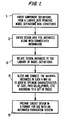
- Figure 1 is a block diagram of the method for synthesizing a circuit according to the related art.
- Figure 2 is a block diagram showing the method for synthesizing a logic circuit design capable of utilizing the present invention.
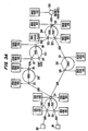
- Figure 3A is a generalized block diagram of a circuit illustrating the calculation of the parameters of the present invention.
- Figure 3B illustrates the definitions of quantities associated with selected locations of the circuit being synthesized.
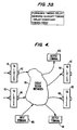
- Figure 4 is a block diagram illustrating the application of the present invention to a circuit including latch circuit elements activated by clock signals.
- Figure 5 is a flow chart describing the computation of parameters associated with selected locations in the circuit and the application of these parameters.
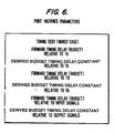
- Figure 6 illustrates the possible timing parameters associated with a port instances of a circuit design according to the present invention.
- Fig. 1 has previously been described in relation to the related art.
- step 21 abstract component data from a library of such data is entered into model definition data structures of the synthesis procedure.
- step 22 component data relating to the target technology from the library is entered into model definition data structures of the synthesis procedure.
- the circuit design data with the connected model instances described in terms of abstract components is entered into the synthesis procedure in step 23.
- step 24 the synthesis procedure provides two sets of pointers. The first set of pointers permits the synthesis procedure to follow any arbitrary path through the design circuit. The second set of pointers couples rules with associated data base structures.
- step 25 the associated rules are tested for each instance and when the test provides a 'true' result, the consequences of the rule is implemented.
- each rule has an antecedent portion and a consequence portion.
- the antecedent portion includes a test algorithm, and the consequence portion provides the information required to implement a result of the test. Because the rules are applied to instances in a sequential manner, and because in the preferred embodiment the test procedures can involve neighboring instances that were changed as a result of a test applied to that instance, the process is repeated until the circuit design has stabilized. In step 27, the final version of the circuit design is placed in a format suitable for use in an automated circuit fabrication system.
- FIG. 3 the technique for establishing a criterion for use in synthesizing the designed circuit is shown.
- a group of group of model instances 350 - 354 are being used as the basis for synthesizing the circuit.
- Associated with each model instance is at least one input terminal and at least one output terminal.
- model instance 350 has input terminals 312 and 313 and an output terminal 314.
- the files of the program associated with each model instance has stored therein data related to the delay of the elements and this information is displayed in Fig. 3.
- the data files associated with model instance 350 has a 1000 unit delay between input terminal 312 and output terminal 314, while model instance 350 has a delay of 1500 units between input terminal 313 and output terminal 314.
- the delay between terminals is also stored in the appropriate files and is illustrated in Fig. 3 by a number between terminals.
- the time delay between input terminal 310 and terminal 312 of model instance 350 is 500 units In Fig. 3, each terminal has associated therewith a group of three numbers, the interpretation of which is illustrated in Fig. 3B.
- the first number is the total time delay from the input terminal.
- the media delay is 500 units. Therefore, the first number in the group of numbers associated with terminal 314 is 500.
- a signal is next delayed by 1000 units by the model instance 350 between input terminal 312 and output terminal 314. Therefore, the first number associated with the path between terminal 310 and terminal 314 is 1500, i.e.
- the forward time delay in the path from input terminal 311 to the output terminal 314 of model instance 350 is given by 2100 units, i.e., 600 units of media delay between terminal 311 and terminal 313 plus 1500 units of model instance delay between terminal 313 and terminal 314.
- the longest delay is chosen to provide consistent results.
- the second number associated with each terminal in Fig. 3B is the derived budget timing delay constant. This reverse time delay is determined in the following manner. At an output terminal 325, a time budget is associated therewith. This time budget is the time delay permitted or preestablished by the circuit design.
- the time delay budget for the circuit illustrated in Fig. 3A is 9000 units. Beginning with the delay time requirement for the output terminal(s), the time delays associated with the model instances and the media delays of the intervening paths are subtracted from the time delay budget or requirement to provide the derived budget timing delay constant or second number (of Fig. 3B) associated with each terminal. By way of further illustration at the output terminal 325, the second number or reverse time delay is 9000 units, the budget or required time delay.
- the output terminal of the model instance 354 the derived budget timing delay constant is 8400 units, the difference between 9000 units at the output terminal and the 600 unit media time delay.
- the derived budget delay constant at terminal 323 of model instance 354 is 4900 units, the difference between the derived timing delay constant of 8400 units at terminal 324 and the delay of 3500 units of the model instance 354 on this signal path.
- a third quantity referred in Fig. 3B as the timing debt is an indication of the actual delay versus the required delay and is determined by subtracting the forward time delay from the derived budget timing delay constant.
- the timing debt at the output of model instance 352 is 200 units, i.e. 4600 units minus 4400 units.
- the timing debt a terminal 314 is 1500 units minus 1700 units or minus 200 units.
- the minus quantity indicates that, at that position of the path, the signal is being delayed by an amount that will not impact the delay of the signal in meeting the timing budget.
- an input terminal includes a signal that is not relevant to the timing delays of the circuit. This signal can generally be referred to as a "don't care" signal and is ignored by the program.
- a generalized block diagram for a portion of the circuit that includes latch elements activated by clock signals is shown.
- the signals from one set of latches 41 and 43, activated by a clock signal TA, must be received by the latches 47 and 49 when the latches 47 and 49 are activated at a second clock signal TB.
- the clock signal TB will have a predetermined delay as compared to clock signal TA, i.e., the TB equal TA + N.
- the signals must pass through the network to be synthesized, illustrated as portion 45. N, the difference between the clock signal TB and the clock signal TA, can serve the same function as the timing budget in the discussion related to Fig. 3A.
- the forward time delays can be computed from the output terminals 42 and 44 of latch elements 41 and 42 respectively to the input terminals 46 and 48 of latch element 47 and 49 respectively.
- N TB - TA can be used as figure of merit, being the difference between as the budget time delay at terminals 46 and 48 of the latches activated by the TB clock signal and the derived budget timing delay constant associated with the model instances of in the network portion 45.
- the timing debt can be determined for each model instance and the timing debt can be used in determining the course of the synthesis procedure activity.
- the circuit instances in network 45 can have timing data associated with input terminals 401 and output terminals 410 and 411.
- step 51 the forward timing delays are calculated for a given location in the circuit by adding together the individual timing delays of model instances and media timing delays between an input terminal or synchronized input terminals and the given location. In the event that a plurality of values for the timing delays are available, the worst possible timing delay is associated with the given location as the forward timing delay.
- step 52 the derived budget timing delay constant is calculated by taking the required or budget timing delay associated with an output terminal or output terminals and subtracting the timing delays of the model instances and media between the given location and the output terminal from the budget timing delay.
- step 53 the timing debt for each given location is determined by subtracting the forward timing delay from the derived budget timing delay constant.
- the circuit is synthesized and model instances resulting from the synthesis have as a least one criterion, the effect of the synthesis on the timing debt a each given location.
- the timing debts are again calculated and the synthesis is repeated. This process is repeated until no change in the circuit design will result from the synthesis procedure.
- the timing delays at the output terminals can be compared with the budget timing delays to determine if the resulting circuit is acceptable.
- the timing parameters that can be associated with a port instance in the circuit design is illustrated.
- the example involves a latch type system having two system clock signals, TA and TB.
- the port instance can be associated with the input or output terminals of a component (or instance of the circuit design).
- the stored parameters include a forward timing delay relative to a path from a TA latch, a derived budget timing delay constant relative to the arrival of a signal along a reverse path direction relative to a TB latch, a forward timing delay relative to a signal originating at a TB latch, a derived budget timing delay constant relative to a signal arriving at a TA latch, a forward timing delay relative to an input terminal and a derived budget timing delay constant relative to output terminals.
- the timing debt is the worst case of the result of subtracting a derived budget timing delay constant from a forward timing delay.
- the procedure that can utilize the present invention most advantageous can typically examine a plurality of circuit design criteria to determine which possible synthesis component, if any, is to replace the original component.
- a plurality of components can acceptable as synthesis components and a priority procedure is imposed to determine which synthesis component, if any, is to replace the present component in the circuit.
- the timing debt at each location can be incorporated as an additional priority factor as the sole criterion for the selection of a replacement synthesis component.
- the priority for circuit synthesis can be imposed that, for any model instances or combination of model instances resulting from the synthesis, the timing budget be reduced when such a new synthesis model instance replaces an original model instance.
- the timing debt parameter also provides a convenient quantity for identifying where the major unacceptable delays are found.
- a port instance can have a plurality of forward and reverse timing delays, each associated with a different path in the design circuit.
- Timing debt is stored with each selected location, however, a multiplicity of data groups shown in Fig. 3B, one of reach path, can be associated with the selected location.
- the procedure herein described becomes progressively longer to execute as the multiplicity of possible paths increases.
- the circuit to be synthesized has latches that are activated by clock signals, then the analysis can be performed form the clock signal driven latch element to clock signal driven latch element, the timing delay between the clock signals can be used in a manner as the budget timing delay for the latch receiving the delayed signal.
- the timing debt can be determined for each location and the timing debt can then be used as one of the criterion by which the synthesis is the logic circuit is controlled.
- Timing information with respect to input signal terminal and output signal terminals can be associated with each port instance. The parameters associated with each port instance in the situation illustrated by Fig. 4 are shown in Fig. 6.
- each port instance therefore has reduced number of timing parameters associated therewith as compared with the situation in which the timing delay parameters are associated with a multiplicity of paths intersecting the port instance. In this manner greatly expanded circuit designs can be analyzed with respect to timing delays.
- the present invention can work most advantageously with a synthesis system that permits the following of circuit paths in a forward or reverse direction relative to the signal flow direction and having the capability of storing potentially large data structures in association with appropriate (terminal and component port) locations.
- the existence of a process for following a signal path in the reverse direction permits the calculation of the reverse time delay without a complicated procedure.
Landscapes
- Engineering & Computer Science (AREA)
- Computer Hardware Design (AREA)
- Physics & Mathematics (AREA)
- Theoretical Computer Science (AREA)
- Evolutionary Computation (AREA)
- Geometry (AREA)
- General Engineering & Computer Science (AREA)
- General Physics & Mathematics (AREA)
- Logic Circuits (AREA)
- Tests Of Electronic Circuits (AREA)
- Recording Measured Values (AREA)
- Image Generation (AREA)
- Apparatus For Radiation Diagnosis (AREA)
- Stereophonic System (AREA)
- Design And Manufacture Of Integrated Circuits (AREA)
- Image Processing (AREA)
- Medicines That Contain Protein Lipid Enzymes And Other Medicines (AREA)
- Peptides Or Proteins (AREA)
Claims (8)
- Verfahren zum Einbringen von Timing-Information in eine Schaltkreissyntheprozedur, die von einem Datenverarbeitungssystem mit einem Speicher ausgeführt wird, wobei die Prozedur eine Schaltkreisrepräsentation benutzt, welche in dem Speicher gespeichert ist, welche einen Haupteingangsanschluß (310), einen Hauptausgangsanschluß (325) und eine Vielzahl von miteinander verbundenen Schaltkreisplätzen, enthaltend eine Vielzahl von Modellbeispielen (model instances) (350-354), die zumindest einen Eingangsanschluß (312; 313: 315: 320: 322, 323; 317, 319) und zumindest einen Ausgangsanschluß (314, 316, 321, 318, 324), die mit diesen assoziiert sind, aufweist und zumindest ein Modellbeispiel (model instance) (350, 354) aufweist, welches zumindest zwei Eingangsanschlüsse (312, 313; 322, 323) und zumindest einen Ausgangsanschluß (314, 324) aufweist, wobei die Timing-Information in dem Speicher gespeichert ist, und für zumindest einen Eingangsanschluß und einen Ausgangsanschluß für jeden aus der Vielzahl von ausgewählten Schaltkreisplätzen der Schaltkreisrepräsentation zumindest einen vorbestimmten Modellbeispiel-Verzögerungswert enthält, welcher eine Timing-Verzögerung innerhalb des Modellbeispiels (model instance) der Schaltkreisrepräsentation repräsentiert, und zumindest einen vorgegebenen mittleren Verzögerungswert enthält, welcher die Timing-Verzögerung zwischen den Anschlüssen unterschiedlicher Modellbeispiele der Schaltkreisrepräsentation repräsentiert und weiterhin für zumindest zwei Eingangsanschlüsse (312, 313; 322, 323) und den zumindest einen Ausgangsanschluß des zumindest einen Modellbeispiels (350, 354) zumindest zwei vorgegebene Modellbeispiel-Verzögerungs- werte enthält, welche die Zeitverzögerungen repräsentieren, die mit den unterschiedlichen Eingangsanschlüssen assoziiert sind und zumindest einen vorgegebenen mittleren Verzögerungswert enthält, welcher eine Timing-Verzögerung zwischen den Anschlüssen unterschiedler Modellbeispiele (model instances) der Schaltkreisrepräsentation repräsentiert, wobei das Verfahren die folgenden Schritte aufweist:
Berechnen einer Vorwärtszeitverzögerung für einen ersten Anschluß eines ausgewählten Schaltkeisplatzes entsprechend jedem Modellbeispiel und eines mittleren Verzögerungswertes, welcher zwischen dem ersten Anschluß und dem Haupteingangsanschluß (310) angeordnet ist, wobei die Vorwärtszeitverzögerung die Zeit repräsentiert, die ein Signal benötigt, um zwischen dem Haupteingangsanschluß der Schaltkreisrepräsentation und des ersten Anschlusses fortzuschreiten; und Ausführen einer entsprechenden Berechnung auch für zumindest ein Modellbeispiel für jeden von zumindest zwei Eingangsanschlüssen,
Zuteilen eines Budget-Zeitverzögerungswertes für den Hauptausgangsanschluß der Schaltkreisrepräsentation, welcher Wert ein Maximum an akzeptierbarer Zeitverzögerung für ein Signal, welches von dem Haupteingangsanschluß an den Hauptausgangsanschluß fortschreitet, repräsentiert;
Berechnen einer erhaltenen Budget-Zeitverzögerungskonstante für den ersten Anschluß eines jeden ausgewählten Schaltkreisplatzes, in dem jedes Modellbeispiel und mittlerer Verzögerungswert zwischen dem ersten Anschluß und dem Hauptausgangsanschluß von dem Budget-Zeitverzögerungswert des Schaltkreisplatzes abgezogen wird; und Ausführen einer entsprechenden Berechnung auch für zumindest ein Modellbeispiel für jeden von seinen zumindest zwei Eingangsanschlüssen,
Berechnen einer Zeitschuld für jeden Anschluß des ausgewählten Schaltkreisplatzes, in dem die erhaltene Budget-Zeitverzögerungskonstante des ersten Anschlusses von der Vorwärtszeitverzögerung des ersten Anschlusses abgezogen wird und in dem eine entsprechende Berechnung auch für zumindest ein Modellbeispiel für jeden dessen zumindest zwei Eingangsanschlüssen ausgeführt wird,
Bestimmen, ob die Schaltkreisrepräsentation, basierend auf einem Wert von zumindest einer der berechneten Zeitschuld, modifiziert werden sollte, und
Modifizieren der Schaltkreisdarstellung, wie sie in dem Speicher gespeichert ist gemäß dem Wert von zumindest einer berechneten Zeitschulden, wenn in dem Bestimmungsschritt bestimmt wurde, daß die Schaltkreisrepräsentation modifiziert werden soll. - Verfahren nach Anspruch 1, bei dem der erste Anschluß von zumindest einem der ausgewählten Schaltkreisplätze relativ zu verschiedenen Punkten in der Schaltkreisrepräsentation eine Vielzahl von berechneten Vorwärtszeitverzögerungen, eine Vielzahl von erhaltenen Budget-Zeitverzögerungskonstanten und eine Vielzahl von Zeitschulden enthält, wobei jede davon dadurch berechnet wird, daß eine der behaltenen Budget-Zeitverzögerungskonstanten des ersten Anschlusses von einer entsprechenden Vorwärtszeitverzögerung des ersten Anschlusses abgezogen wird und wobei das Verfahren weiterhin den Schritt des Auswählens eines der Zeitschulden des ersten Anschlusses als die Zeitschuld aufweist, die zum Bestimmen verwendet wird, ob die Schaltkreisrepräsentation modifiziert werden sollte.
- Verfahren nach Anspruch 1 oder 2, weiterhin enthaltend den Schritt des Ersetzens von zumindest einem ausgewählten Modellbeispiel der Schaltkreisrepräsentation, wie sie in dem Speicher gespeichert ist, durch ein unterschiedliches Modellbeispiel in Antwort auf die Berechnung von zumindest einer der Zeitschulden.
- Verfahren nach Anspruch 2 oder 3, bei dem eine Vielzahl von Timing-Datengruppen enthaltend zumindest eine der Vorwärtszeitverzögerungen, einen der erhaltenen Budget-Zeitverzöge- rungskonstanten und der Zeitschulden mit zumindest einem ausgewählten Schaltkreisplatz der Schaltkreisrepräsentation assoziiert wird, und wobei das Verfahren weiterhin den Schritt des Assoziierens einer jeden aus der Vielzahl von Timing-Gruppen mit einem Schaltkreisplatzverbindungspfad der Schaltkreisrepräsentation aufweist.
- Verfahren nach Anspruch 4, bei dem die Schaltkreisrepräsentation weiterin Latch-Komponenten aufweist, von denen jede zumindest einen der Eingangsanschlüsse und zumindest einen der Ausgangsanschlüsse aufweist.
- Verfahren nach einem der Ansprüche 2 bis 5, bei dem die Schaltkreisrepräsentation weiterhin Latch-Komponenten aufweist, von denen jede zumindest einen der Eingangsanschlüsse und zumindest einen der Ausgangsanschlüsse aufweist und wobei jede Latch-Komponente eine Vielzahl von berechneten Vorwärtszeitverzögerungen aufweist und das Verfahren weiterhin den Schritt des Auswählens der längsten Vorwärtsverzögerungszeit für die Latch-Komponente als die Vorwärtsverzögerungszeit, die für die Berechnung der Zeitschuld für zumindest einen der Anschlüsse der Latch-Komponente verwendet wird, aufweist.
- Verfahren nach einem der Ansprüche 4 bis 6, bei dem die Vielzahl von Timing-Datengruppen, die mit jedem ausgewählten Schaltkreisplatz assoziiert sind, weiterhin die Zeitverzögerungsinformation für eine getaktete Latch-Komponente enthält.
- Verfahren nach einem der Ansprüche 1 bis 7, bei dem die verbundenen Schaltkreisplätze in jede beliebige Richtung durch die Syntheseprozedur durchlaufen werden können.
Applications Claiming Priority (2)
| Application Number | Priority Date | Filing Date | Title |
|---|---|---|---|
| US90751486A | 1986-09-12 | 1986-09-12 | |
| US907514 | 2001-07-16 |
Publications (3)
| Publication Number | Publication Date |
|---|---|
| EP0259705A2 EP0259705A2 (de) | 1988-03-16 |
| EP0259705A3 EP0259705A3 (en) | 1990-10-03 |
| EP0259705B1 true EP0259705B1 (de) | 1994-09-28 |
Family
ID=25424232
Family Applications (1)
| Application Number | Title | Priority Date | Filing Date |
|---|---|---|---|
| EP87112428A Expired - Lifetime EP0259705B1 (de) | 1986-09-12 | 1987-08-26 | Verfahren zur Aufnahme von Zeitparametern in der Synthesis von logischen Schaltungsentwürfen |
Country Status (8)
| Country | Link |
|---|---|
| EP (1) | EP0259705B1 (de) |
| JP (1) | JPS63155268A (de) |
| AT (1) | ATE112403T1 (de) |
| AU (1) | AU7728387A (de) |
| DE (1) | DE3750602T2 (de) |
| DK (1) | DK473587A (de) |
| FI (1) | FI873922A7 (de) |
| IL (1) | IL83618A (de) |
Cited By (1)
| Publication number | Priority date | Publication date | Assignee | Title |
|---|---|---|---|---|
| DE10101540A1 (de) * | 2001-01-15 | 2002-08-01 | Infineon Technologies Ag | Verfahren zur Bestimmung des kritischen Pfades einer integrierten Schaltung |
Families Citing this family (2)
| Publication number | Priority date | Publication date | Assignee | Title |
|---|---|---|---|---|
| US5003487A (en) * | 1988-06-28 | 1991-03-26 | International Business Machines Corporation | Method and apparatus for performing timing correction transformations on a technology-independent logic model during logic synthesis |
| US5210700A (en) * | 1990-02-20 | 1993-05-11 | International Business Machines Corporation | Automatic delay adjustment for static timing analysis |
Family Cites Families (1)
| Publication number | Priority date | Publication date | Assignee | Title |
|---|---|---|---|---|
| US4263651A (en) * | 1979-05-21 | 1981-04-21 | International Business Machines Corporation | Method for determining the characteristics of a logic block graph diagram to provide an indication of path delays between the blocks |
-
1987
- 1987-08-20 AU AU77283/87A patent/AU7728387A/en not_active Abandoned
- 1987-08-23 IL IL83618A patent/IL83618A/xx not_active IP Right Cessation
- 1987-08-26 AT AT87112428T patent/ATE112403T1/de not_active IP Right Cessation
- 1987-08-26 DE DE3750602T patent/DE3750602T2/de not_active Expired - Fee Related
- 1987-08-26 EP EP87112428A patent/EP0259705B1/de not_active Expired - Lifetime
- 1987-09-10 FI FI873922A patent/FI873922A7/fi not_active Application Discontinuation
- 1987-09-11 DK DK473587A patent/DK473587A/da not_active Application Discontinuation
- 1987-09-11 JP JP62226728A patent/JPS63155268A/ja active Pending
Non-Patent Citations (1)
| Title |
|---|
| IEEE 20TH DESIGN AUTOMATION CONFERENCE 1983, paper 27.3, pages 411-418; N.P.JOUPPI: "Timing analysis for nMOS VLSI" * |
Cited By (2)
| Publication number | Priority date | Publication date | Assignee | Title |
|---|---|---|---|---|
| DE10101540A1 (de) * | 2001-01-15 | 2002-08-01 | Infineon Technologies Ag | Verfahren zur Bestimmung des kritischen Pfades einer integrierten Schaltung |
| US7096443B2 (en) | 2001-01-15 | 2006-08-22 | Infineon Technologies Ag | Method for determining the critical path of an integrated circuit |
Also Published As
| Publication number | Publication date |
|---|---|
| DK473587D0 (da) | 1987-09-11 |
| EP0259705A3 (en) | 1990-10-03 |
| DK473587A (da) | 1988-03-13 |
| FI873922A7 (fi) | 1988-03-13 |
| JPS63155268A (ja) | 1988-06-28 |
| IL83618A0 (en) | 1988-01-31 |
| EP0259705A2 (de) | 1988-03-16 |
| FI873922A0 (fi) | 1987-09-10 |
| DE3750602D1 (de) | 1994-11-03 |
| IL83618A (en) | 1991-08-16 |
| DE3750602T2 (de) | 1995-03-09 |
| AU7728387A (en) | 1988-03-17 |
| ATE112403T1 (de) | 1994-10-15 |
Similar Documents
| Publication | Publication Date | Title |
|---|---|---|
| US5168455A (en) | Procedure for incorporating timing parameters in the synthesis of logic circuit designs | |
| US5251147A (en) | Minimizing the interconnection cost of electronically linked objects | |
| US5210700A (en) | Automatic delay adjustment for static timing analysis | |
| US5437007A (en) | Control sequencer in an iconic programming system | |
| Hitchcock et al. | A method of automatic data path synthesis | |
| US5287289A (en) | Logic synthesis method | |
| US4263651A (en) | Method for determining the characteristics of a logic block graph diagram to provide an indication of path delays between the blocks | |
| US5333032A (en) | Logic design system and method in the same | |
| US5113352A (en) | Integrating the logical and physical design of electronically linked objects | |
| US20050066297A1 (en) | System and method for correlated process pessimism removal for static timing analysis | |
| US7346872B2 (en) | Functional timing analysis for characterization of virtual component blocks | |
| EP0814420A1 (de) | Interaktiver cad-apparat zum entwerfen des zusammenbaus von logischen schaltungen | |
| US4922445A (en) | Logic circuit simulation method | |
| US6145116A (en) | Layout design apparatus | |
| US6907590B1 (en) | Integrated circuit design system and method for reducing and avoiding crosstalk | |
| US20050081171A1 (en) | Timing analysis apparatus, timing analysis method and program product | |
| US6697981B2 (en) | System and method for evaluating the location of a failure in a logic circuit, and machine-readable recording medium having a recorded program | |
| EP0259705B1 (de) | Verfahren zur Aufnahme von Zeitparametern in der Synthesis von logischen Schaltungsentwürfen | |
| US6308305B1 (en) | Method and apparatus for circuit designing of an LSI circuit without error paths | |
| Yalcin et al. | An approximate timing analysis method for datapath circuits | |
| US3684871A (en) | Network plotting system | |
| US5490082A (en) | Method of graphically designing circuits | |
| Nagle | Automatic synthesis of microcontrollers | |
| US5796622A (en) | Apparatus for logical simulation and method for producing logical circuit data | |
| Wang et al. | A sequential circuit fault simulation by surrogate fault propagation |
Legal Events
| Date | Code | Title | Description |
|---|---|---|---|
| PUAI | Public reference made under article 153(3) epc to a published international application that has entered the european phase |
Free format text: ORIGINAL CODE: 0009012 |
|
| AK | Designated contracting states |
Kind code of ref document: A2 Designated state(s): AT BE CH DE ES FR GB GR IT LI LU NL SE |
|
| PUAL | Search report despatched |
Free format text: ORIGINAL CODE: 0009013 |
|
| AK | Designated contracting states |
Kind code of ref document: A3 Designated state(s): AT BE CH DE ES FR GB GR IT LI LU NL SE |
|
| 17P | Request for examination filed |
Effective date: 19910319 |
|
| 17Q | First examination report despatched |
Effective date: 19920716 |
|
| GRAA | (expected) grant |
Free format text: ORIGINAL CODE: 0009210 |
|
| AK | Designated contracting states |
Kind code of ref document: B1 Designated state(s): AT BE CH DE ES FR GB GR IT LI LU NL SE |
|
| PG25 | Lapsed in a contracting state [announced via postgrant information from national office to epo] |
Ref country code: NL Effective date: 19940928 Ref country code: LI Effective date: 19940928 Ref country code: GR Free format text: LAPSE BECAUSE OF FAILURE TO SUBMIT A TRANSLATION OF THE DESCRIPTION OR TO PAY THE FEE WITHIN THE PRESCRIBED TIME-LIMIT Effective date: 19940928 Ref country code: CH Effective date: 19940928 Ref country code: BE Effective date: 19940928 Ref country code: AT Effective date: 19940928 |
|
| REF | Corresponds to: |
Ref document number: 112403 Country of ref document: AT Date of ref document: 19941015 Kind code of ref document: T |
|
| REF | Corresponds to: |
Ref document number: 3750602 Country of ref document: DE Date of ref document: 19941103 |
|
| ITF | It: translation for a ep patent filed | ||
| ET | Fr: translation filed | ||
| PG25 | Lapsed in a contracting state [announced via postgrant information from national office to epo] |
Ref country code: SE Effective date: 19941228 |
|
| PG25 | Lapsed in a contracting state [announced via postgrant information from national office to epo] |
Ref country code: ES Free format text: LAPSE BECAUSE OF FAILURE TO SUBMIT A TRANSLATION OF THE DESCRIPTION OR TO PAY THE FEE WITHIN THE PRESCRIBED TIME-LIMIT Effective date: 19950108 |
|
| REG | Reference to a national code |
Ref country code: CH Ref legal event code: PL |
|
| NLV1 | Nl: lapsed or annulled due to failure to fulfill the requirements of art. 29p and 29m of the patents act | ||
| PGFP | Annual fee paid to national office [announced via postgrant information from national office to epo] |
Ref country code: LU Payment date: 19950701 Year of fee payment: 9 |
|
| PGFP | Annual fee paid to national office [announced via postgrant information from national office to epo] |
Ref country code: NL Payment date: 19950719 Year of fee payment: 9 |
|
| PLBE | No opposition filed within time limit |
Free format text: ORIGINAL CODE: 0009261 |
|
| STAA | Information on the status of an ep patent application or granted ep patent |
Free format text: STATUS: NO OPPOSITION FILED WITHIN TIME LIMIT |
|
| PGFP | Annual fee paid to national office [announced via postgrant information from national office to epo] |
Ref country code: ES Payment date: 19950809 Year of fee payment: 9 |
|
| 26N | No opposition filed | ||
| PG25 | Lapsed in a contracting state [announced via postgrant information from national office to epo] |
Ref country code: LU Free format text: LAPSE BECAUSE OF NON-PAYMENT OF DUE FEES Effective date: 19960826 |
|
| PGFP | Annual fee paid to national office [announced via postgrant information from national office to epo] |
Ref country code: FR Payment date: 19980720 Year of fee payment: 12 |
|
| PGFP | Annual fee paid to national office [announced via postgrant information from national office to epo] |
Ref country code: GB Payment date: 19980724 Year of fee payment: 12 |
|
| PGFP | Annual fee paid to national office [announced via postgrant information from national office to epo] |
Ref country code: DE Payment date: 19980729 Year of fee payment: 12 |
|
| PG25 | Lapsed in a contracting state [announced via postgrant information from national office to epo] |
Ref country code: GB Free format text: LAPSE BECAUSE OF NON-PAYMENT OF DUE FEES Effective date: 19990826 |
|
| GBPC | Gb: european patent ceased through non-payment of renewal fee |
Effective date: 19990826 |
|
| PG25 | Lapsed in a contracting state [announced via postgrant information from national office to epo] |
Ref country code: FR Free format text: LAPSE BECAUSE OF NON-PAYMENT OF DUE FEES Effective date: 20000428 |
|
| PG25 | Lapsed in a contracting state [announced via postgrant information from national office to epo] |
Ref country code: DE Free format text: LAPSE BECAUSE OF NON-PAYMENT OF DUE FEES Effective date: 20000601 |
|
| REG | Reference to a national code |
Ref country code: FR Ref legal event code: ST |
|
| PG25 | Lapsed in a contracting state [announced via postgrant information from national office to epo] |
Ref country code: IT Free format text: LAPSE BECAUSE OF NON-PAYMENT OF DUE FEES;WARNING: LAPSES OF ITALIAN PATENTS WITH EFFECTIVE DATE BEFORE 2007 MAY HAVE OCCURRED AT ANY TIME BEFORE 2007. THE CORRECT EFFECTIVE DATE MAY BE DIFFERENT FROM THE ONE RECORDED. Effective date: 20050826 |