EP0258874A2 - An object detecting switch - Google Patents
An object detecting switch Download PDFInfo
- Publication number
- EP0258874A2 EP0258874A2 EP87112745A EP87112745A EP0258874A2 EP 0258874 A2 EP0258874 A2 EP 0258874A2 EP 87112745 A EP87112745 A EP 87112745A EP 87112745 A EP87112745 A EP 87112745A EP 0258874 A2 EP0258874 A2 EP 0258874A2
- Authority
- EP
- European Patent Office
- Prior art keywords
- gate
- signal
- circuit
- transducer
- switch device
- Prior art date
- Legal status (The legal status is an assumption and is not a legal conclusion. Google has not performed a legal analysis and makes no representation as to the accuracy of the status listed.)
- Withdrawn
Links
Images


Classifications
-
- G—PHYSICS
- G01—MEASURING; TESTING
- G01S—RADIO DIRECTION-FINDING; RADIO NAVIGATION; DETERMINING DISTANCE OR VELOCITY BY USE OF RADIO WAVES; LOCATING OR PRESENCE-DETECTING BY USE OF THE REFLECTION OR RERADIATION OF RADIO WAVES; ANALOGOUS ARRANGEMENTS USING OTHER WAVES
- G01S15/00—Systems using the reflection or reradiation of acoustic waves, e.g. sonar systems
- G01S15/02—Systems using the reflection or reradiation of acoustic waves, e.g. sonar systems using reflection of acoustic waves
- G01S15/06—Systems determining the position data of a target
- G01S15/08—Systems for measuring distance only
- G01S15/10—Systems for measuring distance only using transmission of interrupted, pulse-modulated waves
- G01S15/18—Systems for measuring distance only using transmission of interrupted, pulse-modulated waves wherein range gates are used
-
- G—PHYSICS
- G01—MEASURING; TESTING
- G01S—RADIO DIRECTION-FINDING; RADIO NAVIGATION; DETERMINING DISTANCE OR VELOCITY BY USE OF RADIO WAVES; LOCATING OR PRESENCE-DETECTING BY USE OF THE REFLECTION OR RERADIATION OF RADIO WAVES; ANALOGOUS ARRANGEMENTS USING OTHER WAVES
- G01S15/00—Systems using the reflection or reradiation of acoustic waves, e.g. sonar systems
- G01S15/02—Systems using the reflection or reradiation of acoustic waves, e.g. sonar systems using reflection of acoustic waves
- G01S15/04—Systems determining presence of a target
-
- Y—GENERAL TAGGING OF NEW TECHNOLOGICAL DEVELOPMENTS; GENERAL TAGGING OF CROSS-SECTIONAL TECHNOLOGIES SPANNING OVER SEVERAL SECTIONS OF THE IPC; TECHNICAL SUBJECTS COVERED BY FORMER USPC CROSS-REFERENCE ART COLLECTIONS [XRACs] AND DIGESTS
- Y10—TECHNICAL SUBJECTS COVERED BY FORMER USPC
- Y10S—TECHNICAL SUBJECTS COVERED BY FORMER USPC CROSS-REFERENCE ART COLLECTIONS [XRACs] AND DIGESTS
- Y10S367/00—Communications, electrical: acoustic wave systems and devices
- Y10S367/901—Noise or unwanted signal reduction in nonseismic receiving system
-
- Y—GENERAL TAGGING OF NEW TECHNOLOGICAL DEVELOPMENTS; GENERAL TAGGING OF CROSS-SECTIONAL TECHNOLOGIES SPANNING OVER SEVERAL SECTIONS OF THE IPC; TECHNICAL SUBJECTS COVERED BY FORMER USPC CROSS-REFERENCE ART COLLECTIONS [XRACs] AND DIGESTS
- Y10—TECHNICAL SUBJECTS COVERED BY FORMER USPC
- Y10S—TECHNICAL SUBJECTS COVERED BY FORMER USPC CROSS-REFERENCE ART COLLECTIONS [XRACs] AND DIGESTS
- Y10S367/00—Communications, electrical: acoustic wave systems and devices
- Y10S367/903—Transmit-receive circuitry
Definitions
- an object detecting switch device which can detect an object located at a short distance, as well as at a long distance.
- the suppressing gate circuit 4 provides the amplifier 31 with a suppressing signal "b" during a period corresponding to an echo from a gate signal "a” provided by the transmitting gate circuit 11.
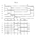
- the signal processing circuit 5 has a short-distance gate 52 and a long-distance gate 51 which, in turn, can receive a gate signal "a" from the transmitting gate circuit 11. Both gates 51 and 52 provide gate signals “c” and “d”, respectively, which rise with gate signal "a” and fall on 5 and 15 cm., respectively, as shown in Fig. 2.
- the gate signals "a”, “b”, “c”, and “d” have respective fixed gate timing periods.
- gate signals "e”. "f”, and “g” rise on 5 cm., 10 cm., and 15 cm., respectively, while falling on detecting ranges designated as “n”, “2n”, and “3n”, respectively (wherein “n” is less than 10 cm.), which are variable according to detecting ranges.
- the gate signal "e” is suppressed by suppress signal "b” so that wave forming circuit 33 does not receive any pulse signals and output Q of flip-flop circuit 57 stays low.
- the second reflective signal returns at the point of 14 cm., designated as "i” in Fig. 2, whereby gate signal “f” is high so that flip-flop circuit 56 is set to make its output Q high, designated as "j” in Fig. 2.
- the AND gate 60 provides an output "k” at the distance of 15 cm., wherein gate signal “g” becomes high. The output "k” remains high up to the point of 24 cm., wherein gate signal "g” goes down.
- the output "k” remains high up to 30 cm., wherein gate signal “g” goes down.
- the second reflective signal “i” comes in at the point of 28 cm., wherein flip-flop circuit 58 is set to provide a signal "l".
- the signal "l” is inputted into flip-flop circuit 59 through the OR gate 61, in order to produce a detecting signal "o".
- presetting of gate timings using preset circuit 6 is performed so that gate signals "e", "f", and “g" have opening periods of 5 to 20 cm., 10 to 20 cm., and 15 to 30 cm., respectively.
Abstract
Description
- This invention relates to an object detecting switch device. More particularly, the invention relates to an object detecting switch device which makes use of a common transducer for transmission and reception of ultrasonic signals.
- Conventionally, an ultrasonic switch device transmits and receives ultrasonic signals to and from an object to be detected. However, this kind of ultrasonic switch produces echoes which prevents the switch from detecting the object unless the object is located close enough to reflect the ultrasonic signals within the range of the echoes.
- In order to detect a short-distant object having reflective ultrasonic signals within the range of the echoes, the distance of the object is calculated by measuring a time period between first and second receiving signals. In another manner, a detection signal is produced if a signal is received during the opening period of a gate.
- As illustrated in Figs. 5(A) and 5(B), immediately after an echo E, it is impossible to determine whether or not a receiving signal is a first receiving signal unless a second receiving signal arrives. In Fig. 5(A), an object is shown to be in a location of 12 cm., while in Fig. 5(B) the object is shown at a distance of 6 cm. away, which is understood by referring to the second and third receiving signals (b2 and b3), respectively.
- For this purpose, however, a detecting gate needs to be kept open for a period corresponding to 40 cm. if a detecting switch is intended for detecting an object located at a distance of 20 cm.. Thus, constant reference to the first and second signals takes time in terms of object detection, and further has the disadvantage of easily picking up noises.
- On the other hand, if reference is made only to the second receiving signal in the detection of an object, signals b1 and b2 cannot be distinguished between a detection range of 8 cm. or 16 cm., as shown in Figs. 6(A) and 6(B). Thus, it is difficult to determine the range of detection displayed on a switch. Further, in Fig. 6(A), in a case wherein a detection gate is set up, for example, between a range of 10 to 15 cm., the detectable ranges are 10 to 15 cm. and 5.0 to 7.5 cm., which results in an undetectable range of 7.5 to 10.0 cm.. Consequently, a noncontinuous range is detected.
- In order to solve the above-described problems, it is a primary object of this invention to provide an object detecting switch device which can detect an object located at a short distance, as well as at a long distance.
- It is another object of this invention to provide an object detecting switch device which avoids picking up noises by shortening the opening time of a detection gate.
- It is still another object of this invention to provide an object detecting switch device which can continuously vary its detecting range.
- In accordance with one embodiment of this invention, there is provided an object detecting switch device which comprises a transducer for emitting and receiving ultrasonic signals to and from an object, a transmitter for driving the transducer, a receiver for receiving a signal from the transducer, a gate for detecting a short-distant object, a gate for detecting a long-distant object, and a circuit for setting the timings of the gates in accordance with the detecting ranges of the object.
- The foregoing and other objects, features and advantages of this invention will be apparent from the following, more particular, description of the preferred embodiments of this invention, as illustrated in the accompanying drawings.
-
- Fig. 1 is a circuit diagram representing an embodiment of an object detecting switch device in accordance with this invention;
- Fig. 2 is a time chart of a wave form under a detecting range of 8 cm. when using the instant invention as shown in Fig. 1;
- Fig. 3 is a time chart of a wave form under a detecting range of 15 cm. when using the instant invention as shown in Fig. 1;
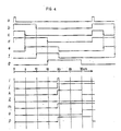
- Fig. 4 is a time chart of a wave form under a detecting range of 20 cm. when using the instant invention as shown in Fig. 1;
- Figs. 5(A) and 5(B) are time charts for use in describing a problem inherent in a conventional detecting switch device; and
- Figs. 6(A) and 6(B) are time charts for use in describing another problem inherent in a conventional detecting switch device.
- Fig. 1 is an embodiment of this invention which comprises a
transmitter 1, an ultrasonic transducer 2 driven by thetransmitter 1, areceiver 3 for receiving a reflected signal, a suppressinggate 4 for suppressing an output ofreceiver 3 during a period corresponding to an echo, asignal processing circuit 5 for processing an output ofreceiver 3 to produce a detection signal, and a preset circuit 6 for presetting the timings of gates contained within thesignal processing circuit 5 in accordance with a detecting range. - The
transmitter 1 comprises atransmitting gate circuit 11, anoscillator 12 which is operable during an open period of the transmittinggate circuit 11, and adrive circuit 13 for driving the transducer 2 by theoscillator 12. - The
receiver 3 comprises anamplifier 31 for amplifying an oscillating signal of the transducer 2, awave detector 32, and awave forming circuit 33 for forming an output pulse of thewave detector 32. - The suppressing
gate circuit 4 provides theamplifier 31 with a suppressing signal "b" during a period corresponding to an echo from a gate signal "a" provided by the transmittinggate circuit 11. - The
signal processing circuit 5 has a short-distance gate 52 and a long-distance gate 51 which, in turn, can receive a gate signal "a" from the transmittinggate circuit 11. Bothgates - The outputs of long-
distance gate 51 and short-distance gate 52 are respectively connected togate pulse generators 53 and 55. The output signal of suppressinggate circuit 4 is also applied to agate pulse generator 54. Thegate pulse generators - The
gate pulse generator 53 provides a gate signal "e" which rises on a falling edge of signal "c" and falls on a detecting range, designated as "n" (see Figure 2), which is preset by preset circuit 6. Thegate pulse generator 54 provides a gate signal "f" which rises on a falling edge of signal "b" and falls on a detecting range, designated as "2n". The pulse generator 55 provides a gate signal "g" which rises on a falling edge of signal "d" and falls on a detecting range, designated as "3n". - Thus, gate signals "e". "f", and "g" rise on 5 cm., 10 cm., and 15 cm., respectively, while falling on detecting ranges designated as "n", "2n", and "3n", respectively (wherein "n" is less than 10 cm.), which are variable according to detecting ranges.
- The output of
wave forming circuit 33 is connected to cp terminals of flip-flop circuits gate pulse generators flop circuits AND gate 60 and a cp terminal of a flip-flop circuit 59 through aninverter 64. An output Q of flip-flop circuit 56 is connected to theAND gate 60 having its output in turn connected to a D terminal of flip-flop circuit 58. An output Q of flip-flop circuit 58 is connected to a D terminal of flip-flop circuit 59 through anOR gate 61 and its output Q' is connected to one input of prohibit gate 62. The other input of prohibit gate 62 is connected from output Q' of flip-flop circuit 56. The output of prohibit gate 62 is connected to anAND gate 63. Another input of theAND gate 63 is provided from an output Q of flip-flop circuit 57. The output of theAND gate 63 is in turn connected to the D terminal of flip-flop circuit 59 through the ORgate 61. - The operation of an embodiment of the object detecting switch device of the instant invention is hereinafter described. The following examples of detecting ranges at 8 cm., 15 cm. and 20 cm. are described for illustrating the operation of the above-discussed embodiment of the object detecting switch device:
- Gate signals "a", "b", "c" and "d" are fixed as shown in Fig. 2. Gate signals "e", "f" and "g" are preset by preset circuit 6 to have opening periods of 5 to 8 cm., 10 to 16 cm., and 15 to 24 cm., respectively.
- Assuming that the distance of an object to be detected is 7 cm., wherein the first reflective signal is obtained within a period of gate signal "e", the gate signal "e" is suppressed by suppress signal "b" so that
wave forming circuit 33 does not receive any pulse signals and output Q of flip-flop circuit 57 stays low. The second reflective signal returns at the point of 14 cm., designated as "i" in Fig. 2, whereby gate signal "f" is high so that flip-flop circuit 56 is set to make its output Q high, designated as "j" in Fig. 2. The ANDgate 60 provides an output "k" at the distance of 15 cm., wherein gate signal "g" becomes high. The output "k" remains high up to the point of 24 cm., wherein gate signal "g" goes down. - The third reflective signal, designated as "i", comes at a distance of 21 cm.. Here, the flip-
flop circuit 58 is set to make its output "l" at a high level based on the output of the ANDgate 60. The output "m" of prohibit gate 62 remains high after the setting of flip-flop circuit 56 and until the setting of flip-flop circuit 58 in which case the signal "l" goes up (see Fig. 2). However, the output signal "m" is low at the point of 24 cm., wherein gate signal "g" goes down. When gate signal "g" goes down, cp terminal of flip-flop circuit 59 is set at a high level throughinverter 64, so that flip-flop circuit 59 is set to provide a detection signal "o", as shown in Figure 2. - In this case, gate signals "e", "f" and "g" are preset to provide gate opening periods of 5 to 15 cm., 10 to 20 cm., and 15 to 30 cm., respectively. Assuming that the distance of an object to be detected is 14 cm., wherein the first reflective signal comes back at a point wherein gate signals "e" and "f" are high and the suppressing gate signal "b" is low, receiving signal "i" is applied from
wave forming circuit 33 to the cp terminals of the flip-flop circuits flop circuits gate 60 provides output "k" when gate signal "g" becomes high at the point of 15 cm.. The output "k" remains high up to 30 cm., wherein gate signal "g" goes down. As illustrated in Fig. 3, the second reflective signal "i" comes in at the point of 28 cm., wherein flip-flop circuit 58 is set to provide a signal "l". At the distance of 30 cm. wherein gate signal "g" goes down, the signal "l" is inputted into flip-flop circuit 59 through theOR gate 61, in order to produce a detecting signal "o". - In this case, presetting of gate timings using preset circuit 6 is performed so that gate signals "e", "f", and "g" have opening periods of 5 to 20 cm., 10 to 20 cm., and 15 to 30 cm., respectively.
- Here, it is assumed that the distance of an object to be detected is 19 cm., wherein the first reflective signal comes in when gate signals "e", "f" and "g" are all high and suppressing signal "b" is low, as illustrated in Fig. 4. Consequently, a reflective signal "i" is provided from
wave forming circuit 33 and inputted to the cp terminals of flip-flop circuits flop circuits - The AND
gate 60 produces output "k" at a distance of 19 cm. which remains at a high level up to 30 cm., wherein gate signal "g" goes down. However, another reflective signal is not received at the cp. terminal of flip-flop circuit 58 which consequently keeps the output Q of flip-flop circuit 58, designated as "l" shown in Fig. 4, at a low level. - On the other hand, when the output Qʹ of the flip-
flop circuit 56 becomes low at the distance of 19 cm., wherein the first reflective signal comes in, the output "m" of the prohibit gate 62 becomes high resulting in the high-state of the ANDgate 63. The high signal from the ANDgate 63 is applied to the D terminal of flip-flop circuit 59 through theOR gate 61, and thereafter inputted into flip-flop circuit 59 in order to produce a detection signal "o" at the point of 30 cm., wherein the gate signal "g" goes down. - In the above-described structural arrangement and operations, in accordance to an embodiment of this invention, it is possible to detect an object not only at a short distance away, but also at a long distance by continuously adjusting the detecting range. Moreover, multiple reflective signals are applied only for detecting a short-distance object, so that it is possible to generally keep reflective signals at high levels. Further, gate opening periods are shorter with the instant invention, thereby significantly reducing the noise being picked up.
- While the invention has been particularly shown and described in reference to preferred embodiments thereof, it will be understood by those skilled in the art that changes in form and details may be made without departing from the spirit and scope of the invention.
Claims (8)
a transducer for emitting and receiving ultrasonic signals to and from an object;
a transmitter for driving the transducer;
a receiver for receiving a signal from the transducer;
a gate for detecting a short-distant object;
a gate for detecting a long-distant object; and
a circuit for setting timings of the gates in accordance with the detecting ranges of the object.
a transmitting gate circuit;
an oscillator which is operable during an open period of the transmitting gate circuit; and
a drive circuit for driving the transducer by the oscillator.
an amplifier for amplifying an oscillating signal of the transducer;
a wave detector; and
a wave forming circuit for forming an output pulse of the wave detector.
a transducer for emitting and receiving ultrasonic signals to and from an object;
a transmitter for driving the transducer;
a receiver for receiving a reflected signal from the transducer;
a gate for suppressing an output of the receiver during a period corresponding to an echo;
a signal processing circuit for processing an output of the receiver for producing a detection signal; and
a preset circuit for presetting the timings of gates contained within the signal processing circuit in accordance with a detecting range.
a transmitting gate circuit;
an oscillator which is operable during an open period of the transmitting gate circuit; and
a drive circuit for driving the transducer by the oscillator.
an amplifier for amplifying an oscillating signal of the transducer;
a wave detector; and
a wave forming circuit for forming an output pulse of the wave detector.
Applications Claiming Priority (2)
| Application Number | Priority Date | Filing Date | Title |
|---|---|---|---|
| JP61207455A JPH06100651B2 (en) | 1986-09-02 | 1986-09-02 | Ultrasonic switch |
| JP207455/86 | 1986-09-02 |
Publications (2)
| Publication Number | Publication Date |
|---|---|
| EP0258874A2 true EP0258874A2 (en) | 1988-03-09 |
| EP0258874A3 EP0258874A3 (en) | 1989-01-18 |
Family
ID=16540053
Family Applications (1)
| Application Number | Title | Priority Date | Filing Date |
|---|---|---|---|
| EP87112745A Withdrawn EP0258874A3 (en) | 1986-09-02 | 1987-09-01 | An object detecting switch |
Country Status (3)
| Country | Link |
|---|---|
| US (1) | US5008862A (en) |
| EP (1) | EP0258874A3 (en) |
| JP (1) | JPH06100651B2 (en) |
Families Citing this family (5)
| Publication number | Priority date | Publication date | Assignee | Title |
|---|---|---|---|---|
| US5177711A (en) * | 1986-09-02 | 1993-01-05 | Omron Tateisi Electronics | Object detecting switch device |
| US5373482A (en) * | 1990-02-26 | 1994-12-13 | Trend Tec Inc. | Distance measuring system arranged to limit false indications of distance measurements |
| US5459698A (en) * | 1993-03-08 | 1995-10-17 | The Rexroth Corporation | Noninvasive ultrasonic proximity detector for a fluid actuated cylinder |
| JP2002090452A (en) * | 2000-09-14 | 2002-03-27 | Nippon Ceramic Co Ltd | Ultrasonic range finder |
| JP5807197B2 (en) * | 2011-04-13 | 2015-11-10 | パナソニックIpマネジメント株式会社 | Object detection device |
Citations (6)
| Publication number | Priority date | Publication date | Assignee | Title |
|---|---|---|---|---|
| US2629867A (en) * | 1943-04-17 | 1953-02-24 | Allen H Schooley | Range aperturing device |
| US3412390A (en) * | 1965-10-14 | 1968-11-19 | Westinghouse Electric Corp | Echo ranging system for monitoring plurality of detection zones to determine presence of absence of objects |
| US3680039A (en) * | 1970-10-08 | 1972-07-25 | Thomas K Tsao | Apparatus for detecting movable objects |
| US3760343A (en) * | 1969-10-20 | 1973-09-18 | Gen Signal Corp | Apparatus for controlling sonic energy distribution |
| US3781772A (en) * | 1972-02-25 | 1973-12-25 | Matsushita Electric Works Ltd | Ultrasonic detection apparatus |
| EP0156636A2 (en) * | 1984-03-22 | 1985-10-02 | Salubre Investments Limited | The processing of reflected signals |
Family Cites Families (8)
| Publication number | Priority date | Publication date | Assignee | Title |
|---|---|---|---|---|
| US4332016A (en) * | 1979-01-26 | 1982-05-25 | A/S Tomra Systems | Method, apparatus and transducer for measurement of dimensions |
| US4326273A (en) * | 1980-07-23 | 1982-04-20 | Hurst Performance, Inc. | Ultrasonic ranging device |
| US4489319A (en) * | 1981-03-06 | 1984-12-18 | Raytheon Company | Detector with variance sensitivity |
| DE3207950A1 (en) * | 1982-03-05 | 1983-09-15 | Bosch Gmbh Robert | DISTANCE MEASURING DEVICE |
| JPS5937459A (en) * | 1982-08-27 | 1984-02-29 | Automob Antipollut & Saf Res Center | Body detector by ultrasonic wave |
| US4679175A (en) * | 1984-12-13 | 1987-07-07 | Honeywell Inc. | Ultrasonic distance sensor with dual burst noise rejection |
| US4717916A (en) * | 1986-05-16 | 1988-01-05 | Holodyne Ltd., 1986 | High resolution imaging doppler interferometer |
| US4785429A (en) * | 1987-03-04 | 1988-11-15 | Folwell Dale E | Range control system |
-
1986
- 1986-09-02 JP JP61207455A patent/JPH06100651B2/en not_active Expired - Lifetime
-
1987
- 1987-09-01 EP EP87112745A patent/EP0258874A3/en not_active Withdrawn
-
1990
- 1990-01-18 US US07/465,603 patent/US5008862A/en not_active Expired - Fee Related
Patent Citations (6)
| Publication number | Priority date | Publication date | Assignee | Title |
|---|---|---|---|---|
| US2629867A (en) * | 1943-04-17 | 1953-02-24 | Allen H Schooley | Range aperturing device |
| US3412390A (en) * | 1965-10-14 | 1968-11-19 | Westinghouse Electric Corp | Echo ranging system for monitoring plurality of detection zones to determine presence of absence of objects |
| US3760343A (en) * | 1969-10-20 | 1973-09-18 | Gen Signal Corp | Apparatus for controlling sonic energy distribution |
| US3680039A (en) * | 1970-10-08 | 1972-07-25 | Thomas K Tsao | Apparatus for detecting movable objects |
| US3781772A (en) * | 1972-02-25 | 1973-12-25 | Matsushita Electric Works Ltd | Ultrasonic detection apparatus |
| EP0156636A2 (en) * | 1984-03-22 | 1985-10-02 | Salubre Investments Limited | The processing of reflected signals |
Also Published As
| Publication number | Publication date |
|---|---|
| JPS6361976A (en) | 1988-03-18 |
| EP0258874A3 (en) | 1989-01-18 |
| US5008862A (en) | 1991-04-16 |
| JPH06100651B2 (en) | 1994-12-12 |
Similar Documents
| Publication | Publication Date | Title |
|---|---|---|
| US4382291A (en) | Surveillance system in which a reflected signal pattern is compared to a reference pattern | |
| DE3176130D1 (en) | Circuit for determining and displaying when the distance between a vehicle and an obstacle falls below predetermined minimum values | |
| US4482889A (en) | Device for detecting failure of ultrasonic apparatus | |
| WO2000005597A3 (en) | Precision short-range pulse-echo systems with automatic pulse detectors | |
| US4622553A (en) | Radar detector | |
| US4914951A (en) | Apparatus for remote distance measurement | |
| US5177711A (en) | Object detecting switch device | |
| US5008862A (en) | Object detecting switch device | |
| JPH02223884A (en) | Moving object detecting device | |
| JP2828678B2 (en) | Ultrasonic detector | |
| US4214314A (en) | Precision transponder and method of communicating therewith | |
| JPS61172085A (en) | Range finding type matter detection apparatus | |
| JP2904391B2 (en) | Ultrasonic sensor | |
| JP3066545B2 (en) | Ultrasonic sensor with intruding object detection function | |
| JPH037827Y2 (en) | ||
| JP2801997B2 (en) | Tidal current measurement method | |
| JPH03180794A (en) | Method and instrument for ultrasonic distance measurement | |
| JPS63128278A (en) | Detector using ultrasonic wave or the like | |
| JPS6147387B2 (en) | ||
| KR860000456B1 (en) | The apparatus for measuring distance | |
| JPS6343718B2 (en) | ||
| JPH0334710Y2 (en) | ||
| JPH0483192A (en) | Ultrasonic sensor | |
| JPH04242189A (en) | Ultrasonic detector | |
| JP2849417B2 (en) | Ultrasonic detector |
Legal Events
| Date | Code | Title | Description |
|---|---|---|---|
| PUAI | Public reference made under article 153(3) epc to a published international application that has entered the european phase |
Free format text: ORIGINAL CODE: 0009012 |
|
| 17P | Request for examination filed |
Effective date: 19870901 |
|
| AK | Designated contracting states |
Kind code of ref document: A2 Designated state(s): AT BE CH DE ES FR GB GR IT LI LU NL SE |
|
| PUAL | Search report despatched |
Free format text: ORIGINAL CODE: 0009013 |
|
| AK | Designated contracting states |
Kind code of ref document: A3 Designated state(s): AT BE CH DE ES FR GB GR IT LI LU NL SE |
|
| 17Q | First examination report despatched |
Effective date: 19901129 |
|
| STAA | Information on the status of an ep patent application or granted ep patent |
Free format text: STATUS: THE APPLICATION HAS BEEN WITHDRAWN |
|
| 18W | Application withdrawn |
Withdrawal date: 19910405 |
|
| R18W | Application withdrawn (corrected) |
Effective date: 19910405 |
|
| RIN1 | Information on inventor provided before grant (corrected) |
Inventor name: SHIMAMOTO, HIROSHIOMRON TATEISI ELECTRONICS CO. Inventor name: YAMAGUCHI, YUKIOOMRON TATEISI ELECTRONICS CO. Inventor name: SUZAKI, HIDEYUKIOMRON TATEISI ELECTRONICS CO. Inventor name: KAWANO, ATUSI OMRON TATEISI ELECTRONICS CO. |