EP0258383B1 - Masked ion beam lithography system and method - Google Patents
Masked ion beam lithography system and method Download PDFInfo
- Publication number
- EP0258383B1 EP0258383B1 EP87901780A EP87901780A EP0258383B1 EP 0258383 B1 EP0258383 B1 EP 0258383B1 EP 87901780 A EP87901780 A EP 87901780A EP 87901780 A EP87901780 A EP 87901780A EP 0258383 B1 EP0258383 B1 EP 0258383B1
- Authority
- EP
- European Patent Office
- Prior art keywords
- lens
- ion
- source
- ions
- magnet
- Prior art date
- Legal status (The legal status is an assumption and is not a legal conclusion. Google has not performed a legal analysis and makes no representation as to the accuracy of the status listed.)
- Expired - Lifetime
Links
- 238000000034 method Methods 0.000 title claims abstract description 24
- 238000002164 ion-beam lithography Methods 0.000 title abstract description 5
- 150000002500 ions Chemical class 0.000 claims abstract description 73
- 238000010884 ion-beam technique Methods 0.000 claims abstract description 43
- 238000000605 extraction Methods 0.000 claims abstract description 29
- 239000002245 particle Substances 0.000 claims abstract description 20
- 239000000758 substrate Substances 0.000 claims abstract description 20
- 230000007246 mechanism Effects 0.000 claims abstract description 15
- 230000005465 channeling Effects 0.000 claims abstract description 13
- 230000003287 optical effect Effects 0.000 claims description 9
- 230000009977 dual effect Effects 0.000 claims description 5
- 230000008569 process Effects 0.000 claims description 5
- 230000005684 electric field Effects 0.000 claims description 4
- 238000004519 manufacturing process Methods 0.000 claims description 4
- 230000003362 replicative effect Effects 0.000 claims description 3
- 238000005468 ion implantation Methods 0.000 abstract description 6
- 239000004065 semiconductor Substances 0.000 abstract description 4
- 210000002381 plasma Anatomy 0.000 description 9
- 230000001133 acceleration Effects 0.000 description 7
- 239000007789 gas Substances 0.000 description 7
- XEEYBQQBJWHFJM-UHFFFAOYSA-N Iron Chemical compound [Fe] XEEYBQQBJWHFJM-UHFFFAOYSA-N 0.000 description 5
- 230000008901 benefit Effects 0.000 description 5
- 239000012212 insulator Substances 0.000 description 5
- 238000001015 X-ray lithography Methods 0.000 description 4
- 230000000694 effects Effects 0.000 description 4
- 238000000609 electron-beam lithography Methods 0.000 description 4
- 239000012535 impurity Substances 0.000 description 4
- 239000000463 material Substances 0.000 description 4
- 238000010521 absorption reaction Methods 0.000 description 3
- 229910052751 metal Inorganic materials 0.000 description 3
- 239000002184 metal Substances 0.000 description 3
- 230000007935 neutral effect Effects 0.000 description 3
- 238000005086 pumping Methods 0.000 description 3
- 238000013461 design Methods 0.000 description 2
- 238000010894 electron beam technology Methods 0.000 description 2
- 230000002708 enhancing effect Effects 0.000 description 2
- 230000004907 flux Effects 0.000 description 2
- 125000004435 hydrogen atom Chemical group [H]* 0.000 description 2
- 229910052742 iron Inorganic materials 0.000 description 2
- 230000000737 periodic effect Effects 0.000 description 2
- 229920002120 photoresistant polymer Polymers 0.000 description 2
- 238000012545 processing Methods 0.000 description 2
- 230000005855 radiation Effects 0.000 description 2
- 238000004544 sputter deposition Methods 0.000 description 2
- 229910052582 BN Inorganic materials 0.000 description 1
- PZNSFCLAULLKQX-UHFFFAOYSA-N Boron nitride Chemical compound N#B PZNSFCLAULLKQX-UHFFFAOYSA-N 0.000 description 1
- OKTJSMMVPCPJKN-UHFFFAOYSA-N Carbon Chemical compound [C] OKTJSMMVPCPJKN-UHFFFAOYSA-N 0.000 description 1
- 229910001209 Low-carbon steel Inorganic materials 0.000 description 1
- 230000009471 action Effects 0.000 description 1
- 238000013459 approach Methods 0.000 description 1
- 230000033228 biological regulation Effects 0.000 description 1
- 230000015572 biosynthetic process Effects 0.000 description 1
- 230000015556 catabolic process Effects 0.000 description 1
- 239000000919 ceramic Substances 0.000 description 1
- 230000008859 change Effects 0.000 description 1
- 238000006243 chemical reaction Methods 0.000 description 1
- 238000001816 cooling Methods 0.000 description 1
- 230000008878 coupling Effects 0.000 description 1
- 238000010168 coupling process Methods 0.000 description 1
- 238000005859 coupling reaction Methods 0.000 description 1
- 230000007812 deficiency Effects 0.000 description 1
- 230000003111 delayed effect Effects 0.000 description 1
- 239000002019 doping agent Substances 0.000 description 1
- 238000010891 electric arc Methods 0.000 description 1
- 230000008030 elimination Effects 0.000 description 1
- 238000003379 elimination reaction Methods 0.000 description 1
- 238000005516 engineering process Methods 0.000 description 1
- 229910002804 graphite Inorganic materials 0.000 description 1
- 239000010439 graphite Substances 0.000 description 1
- 238000010438 heat treatment Methods 0.000 description 1
- 238000002513 implantation Methods 0.000 description 1
- 238000002955 isolation Methods 0.000 description 1
- 239000012528 membrane Substances 0.000 description 1
- 229910021421 monocrystalline silicon Inorganic materials 0.000 description 1
- 238000013021 overheating Methods 0.000 description 1
- 238000000059 patterning Methods 0.000 description 1
- 238000007639 printing Methods 0.000 description 1
- 229910052761 rare earth metal Inorganic materials 0.000 description 1
- 150000002910 rare earth metals Chemical class 0.000 description 1
- 238000007493 shaping process Methods 0.000 description 1
- 239000002904 solvent Substances 0.000 description 1
- 230000006641 stabilisation Effects 0.000 description 1
- 238000011105 stabilization Methods 0.000 description 1
- WFKWXMTUELFFGS-UHFFFAOYSA-N tungsten Chemical compound [W] WFKWXMTUELFFGS-UHFFFAOYSA-N 0.000 description 1
- 229910052721 tungsten Inorganic materials 0.000 description 1
- 239000010937 tungsten Substances 0.000 description 1
Images


Classifications
-
- H—ELECTRICITY
- H01—ELECTRIC ELEMENTS
- H01J—ELECTRIC DISCHARGE TUBES OR DISCHARGE LAMPS
- H01J37/00—Discharge tubes with provision for introducing objects or material to be exposed to the discharge, e.g. for the purpose of examination or processing thereof
- H01J37/30—Electron-beam or ion-beam tubes for localised treatment of objects
- H01J37/317—Electron-beam or ion-beam tubes for localised treatment of objects for changing properties of the objects or for applying thin layers thereon, e.g. for ion implantation
-
- B—PERFORMING OPERATIONS; TRANSPORTING
- B82—NANOTECHNOLOGY
- B82Y—SPECIFIC USES OR APPLICATIONS OF NANOSTRUCTURES; MEASUREMENT OR ANALYSIS OF NANOSTRUCTURES; MANUFACTURE OR TREATMENT OF NANOSTRUCTURES
- B82Y10/00—Nanotechnology for information processing, storage or transmission, e.g. quantum computing or single electron logic
-
- B—PERFORMING OPERATIONS; TRANSPORTING
- B82—NANOTECHNOLOGY
- B82Y—SPECIFIC USES OR APPLICATIONS OF NANOSTRUCTURES; MEASUREMENT OR ANALYSIS OF NANOSTRUCTURES; MANUFACTURE OR TREATMENT OF NANOSTRUCTURES
- B82Y40/00—Manufacture or treatment of nanostructures
-
- H—ELECTRICITY
- H01—ELECTRIC ELEMENTS
- H01J—ELECTRIC DISCHARGE TUBES OR DISCHARGE LAMPS
- H01J37/00—Discharge tubes with provision for introducing objects or material to be exposed to the discharge, e.g. for the purpose of examination or processing thereof
- H01J37/30—Electron-beam or ion-beam tubes for localised treatment of objects
- H01J37/317—Electron-beam or ion-beam tubes for localised treatment of objects for changing properties of the objects or for applying thin layers thereon, e.g. for ion implantation
- H01J37/3174—Particle-beam lithography, e.g. electron beam lithography
-
- H—ELECTRICITY
- H01—ELECTRIC ELEMENTS
- H01J—ELECTRIC DISCHARGE TUBES OR DISCHARGE LAMPS
- H01J2237/00—Discharge tubes exposing object to beam, e.g. for analysis treatment, etching, imaging
- H01J2237/05—Arrangements for energy or mass analysis
- H01J2237/055—Arrangements for energy or mass analysis magnetic
-
- H—ELECTRICITY
- H01—ELECTRIC ELEMENTS
- H01J—ELECTRIC DISCHARGE TUBES OR DISCHARGE LAMPS
- H01J2237/00—Discharge tubes exposing object to beam, e.g. for analysis treatment, etching, imaging
- H01J2237/15—Means for deflecting or directing discharge
- H01J2237/151—Electrostatic means
- H01J2237/1516—Multipoles
-
- H—ELECTRICITY
- H01—ELECTRIC ELEMENTS
- H01J—ELECTRIC DISCHARGE TUBES OR DISCHARGE LAMPS
- H01J2237/00—Discharge tubes exposing object to beam, e.g. for analysis treatment, etching, imaging
- H01J2237/30—Electron or ion beam tubes for processing objects
- H01J2237/303—Electron or ion optical systems
-
- H—ELECTRICITY
- H01—ELECTRIC ELEMENTS
- H01J—ELECTRIC DISCHARGE TUBES OR DISCHARGE LAMPS
- H01J2237/00—Discharge tubes exposing object to beam, e.g. for analysis treatment, etching, imaging
- H01J2237/30—Electron or ion beam tubes for processing objects
- H01J2237/317—Processing objects on a microscale
- H01J2237/3175—Lithography
- H01J2237/31752—Lithography using particular beams or near-field effects, e.g. STM-like techniques
- H01J2237/31755—Lithography using particular beams or near-field effects, e.g. STM-like techniques using ion beams
-
- H—ELECTRICITY
- H01—ELECTRIC ELEMENTS
- H01J—ELECTRIC DISCHARGE TUBES OR DISCHARGE LAMPS
- H01J2237/00—Discharge tubes exposing object to beam, e.g. for analysis treatment, etching, imaging
- H01J2237/30—Electron or ion beam tubes for processing objects
- H01J2237/317—Processing objects on a microscale
- H01J2237/3175—Lithography
- H01J2237/31777—Lithography by projection
- H01J2237/31788—Lithography by projection through mask
Definitions
- This invention relates to the exposure of resists in the formation of integrated circuits, and more particularly to masked ion beam lithography exposure systems and methods.
- Integrated circuits are generally formed with a series of masks that are used to create desired patterns on a semiconductive substrate.
- the substrate is initially coated with a resist material, and a mask carrying a desired pattern is positioned over the coated substrate.
- the substrate is then exposed, fixing the resist except where it has been shaded by the mask pattern.
- the shaded resist is then washed away in a solvent bath, and any underlying layer etched to reveal the substrate (for negative resists, the unexposed portions are washed away).
- Appropriate dopants or materials are next applied to the substrate, followed by the removal of the remaining resist, the application of another resist layer, and another mask iteration. This process continues for successive masks until the circuit pattern has been completed.
- Ultraviolet light is commonly used in conjunction with a photoresist in fabricating integrated circuits. More recently, however, ion beam lithography techniques have been developed in which H + ions are used to expose an ion-sensitive resist material on the semiconductive substrate. Ion exposures yield much higher resolution patterns than those produced by ultraviolet light because, at submicrometer dimensions, light undergoes substantial diffraction whereas ions are not substantially influenced.
- MIBL basic masked ion beam lithography
- Ion implantation accelerators have previously been used for doping semiconductors in the fabricating of integrated circuits. These same machines have also been adapted for experimental use to provide the necessary ion exposure beam for an experimental MIBL system. While convenient because the equipment is already available, ion implantation accelerators are very large and overpowered for ion beam lithographic applications. Serious problems have been encountered in aligning the beam with the mask and the underlying substrate, in providing appropriate beam power, and in the expense of an exposure.
- EBL direct-write electron beam lithography
- XRL x-ray lithography
- focused ion beam microfabrication Each of these techniques has limitations that make a more efficient and practical MIBL system desirable.
- EBL is not well suited for high speed printing in the submicrometer feature size domain because of its slow, serial patterning with a finely focused beam.
- EBL systems used for integrated circuit fabrication are characterized by high cost and complexity, low throughput and marginal resolution.
- XRL for integrated circuit fabrication has been delayed because of low throughput for submicrometer features.
- Another object is the provision of such an MIBL-system and method, in which the ion beam is formed and directed to the mask in an energy efficient manner which utilizes much more of the initial beam current than in previous systems, and in which the beam energy may be conveniently varied.
- a further object is the provision of such a novel and improved system MIBL and method, in which extraneous particles are effectively removed and the beam consists substantially of pure H *- ions.
- a MIBL-system which includes means for holding a lithographic mask in a predetermined position for the respect to a target, an ion source, means for extracting ions from the source and forming them into an expanding beam, and means for substantially collimating the beam toward the mask position.
- a dual electrode extraction mechanism forms H + ions from the source into an initial beam with a predetermined angular divergence, while a first lens positioned in the beam path focuses the beam with an angular convergence substantially greater than its initial divergence, thus amplifying the beam's angular expansion beyond the lens' focal (cross-over) point.
- the beam is then substantially collimated by a second lens which is, positioned beyond the focal point of the first lens at a location corresponding to a desired collimated beam diameter.
- a sector magnet positioned in the beam path between the extraction mechanism and first lens deflects particles in the beam in accordance with their mass. The magnet transmits H + ions along the desired beam path, while deflecting higher mass particles out of the beam.
- An octupole deflector is used to steer the collimated beam into alignment with the channeling axis of the mask.
- the masked beam is received by a resist coated substrate which is aligned with the mask, and means are provided for rapidly moving the substrate relative to the beam for replicating the mask pattern on the substrate.
- the extraction mechanism includes a pair of electrodes spaced in succession from the ion source, with the spacings between electrodes and relative voltages applied to the electrodes designed to extract ions from the source in a beam having a predetermined angle of expansion.
- the electric field strength between the ion source and the nearer electrode is preferably about half of the electric field strength between the nearer and more distant electrodes.
- the first and second lenses each preferably comprise dual cylinder lenses, and include means for establishing predetermined voltage differential ratios across the entrance and exit cylinders of each lens to shape the beam and accelerate the H + ions therein.
- the first lens entrance cylinder is maintained at the same voltage as the exit electrode for the extraction mechanism, while its exit cylinder is maintained at the same voltage as the entrance cylinder for the second lens.
- the voltages of the ion source, extraction electrodes/first lens entrance cylinder, and first lens exit cylinder/ second lens entrance cylinder are preferably maintained within the approximate ranges of 200-300kV, 192-288kV and 160-240kV, respectively, relative to the second lens exit cylinder voltage.
- the absolute values of the voltage differentials across the entrance and exit cylinders of each lens can be varied while retaining the predetermined voltage differential ratios, thus providing control over the beam energy with a simple voltage adjustment.
- the sector magnet is specially designed to preserve an apparent point source for the intial expanding beam and to transmit only H + ions along the desired beam path. It is characterized as a 20° sector electromagnet with a 1.5cm. pole gap, a flat entrance pole face at a tilt angle of substantially +8.2°, and a flat exit pole face at a tilt angle of substantially +5.5°.
- FIG. 1 A schematic-type elevational drawing of an MIBL system contemplated by the present invention is shown in FIG. 1.
- the system features a compact, vertical ion beam column approximately 1.7 meters in total length, which is considerably smaller than prior ion implantation accelerators used for MIBL applications.
- the system is capable of producing an H + ion beam with energies up to 300keV and current densities up to 5J..lA/cm2.
- the MIBL optical column includes a surrounding vacuum enclosure, indicated by reference 2, which provides mechanical support for the various components of the system.
- a surrounding vacuum enclosure indicated by reference 2
- details of the vacuum enclosure are not shown, nor are cooling systems for some of the components or the details of electrical leads.
- a high efficiency H + ion source 4 is located at the top of the column.
- the ion source is of the arc- discharge type with magnetic multiple confinement. This type of device achieves high source efficiency by providing long confinement times for ionizing electrons, while maintaining a major portion of the plasma in an essentially field-free (less than 0.002T (20 Gauss)) region. Such field-free regions are occupied by uniform, quiescent plasmas with low effective plasma temperatures suitable for extracting high optical quality ion beams.
- a small (less than 5mm (0.2")), slowly diverging (less than 15 mrad) beam is extracted from the source by a two-stage extraction mechanism 6. Extractor 6, described in more detail below, regulates the extracted current level by the field in its first stage, and controls the extracted beam divergence predominantly by the field in its second stage.
- the beam After receiving its initial acceleration from extractor 6, the beam is directed to a variable field sector electromagnet 8, which causes the various particles within the beam to be angularly deflected by amounts that vary in proportion to the mass of each particle.
- the magnet is specially designed so that H + ions within the beam are deflected to a desired beam path 10, while heavier ions are deflected by lesser amounts and thereby eliminated from the beam.
- the magnet is further designed to preserve a high quality virtual point source for the beam, which is important in the further manipulation of the beam within the optical column, and also keeps the cross-section of the beam generally circular. The removal of higher mass ions and neutral beam components is necessary to control the resist exposure dose, and to reduce mask heating effects.
- Sector magnet 8 is positioned within the optical column at a location at which the beam has received an initial acceleration but prior to full acceleration to the final desired energy level, since the required magnetic fields at the lower energy location are considerably less.
- the magnet structure can thus be made more compact than would be the case for a magnet capable of handling H + ions with energies up to 300keV.
- the elimination of heavier particles prior to full acceleration reduces the electrical load on the high voltage supplies, and eliminates the radiation background produced by stopping high energy ions.
- the sector magnet is carefully designed so that the beam is matched to the optics of the acceleration stages, described below.
- the essentially pure H + beam is passed through the central aperture of a plate 12 to limit stray ions.
- the radius of the beam at the aperture is limited to about 0.15cm., and its angular divergence is limited to 10mrad.
- An octupole deflector 13 is positioned below aperture plate 12 to provide a mechanism for performing fine adjustments in the alignment of the mass analyzed beam with the optical axis of the column, and in the shape of the beam. This deflector can also be used in effect to periodically turn the beam "off" during the wafer stepping and alignment periods when the MIBL system is used in a high throughput mode.
- the beam is turned “on” only during those periods when actual resist exposure is desired, typically about 0.5 second out of a total 1.5 second step-align-expose cycle.
- Applying an appropriate voltage to octupole 13 deflects the beam out of the column path, in effect "blanking" the beam. While a lesser number of electrodes could be used to accomplish this periodic blanking, an octupole is preferred because the same device can be used to align and shape the beam.
- a DC voltage is applied to the octupole for the aligning and shaping function, with a much higher voltage super-imposed to control beam "blanking".
- the beam Upon emerging from aperture plate 12 and octupole 13 the beam is processed by a pair of dual cylinder lenses 14 and 16.
- the first lens 14 comprises a pair of hollow cylinders 18 and 20, between which a voltage differential is established to focus the beam at an angle of convergence which is at least three times its angular divergence upon entering the lens.
- the second lens 16 consists of another pair of hollow cylinders 22 and 24, between which another voltage differential is established.
- the first lens 14 focuses the beam to a crossover at the focal point of the second lens 16, so that the beam is highly collimated when it emerges from lens 16.
- each lens increases the beam energy by a factor of 5 for a total energy multiplication of 25 (the increase in beam energy by each lens is equal to the ratio of its exit voltage over its entrance voltage, all relative to the ion source voltage).
- the beam crossover point is mechanically limited by an aperture plate 26 on which current can be monitored to control a final adjustment of the first lens 14, fixing its demagnified image at the focal point of the second lens. From the crossover point, the beam expands at an amplified angular divergence compared to its initial divergence until it reaches the principle plane of the second lens 16. At the second lens the H + ions are collimated into a substantially parallel beam, with a divergence of less than 2mrad and a diameter of 1.7cm or greater.
- the use of the demagnifying first lens 14 enables the achievement of a small geometry in the ion source/magnet region by initially generating a small, low divergence beam and then expanding the beam in the first lens acceleration stage to obtain the final beam dimensions.
- the aperture plate 26 at the beam crossover point ensures proper beam optics upon entry to the second lens, while discriminating against any neutral beam components which may have formed between magnet 8 and the first lens 14.
- the overall length of the optical column from the entrance of the first lens to the exit of the second lens is approximately one meter.
- the lenses are thus contained within substantially the maximum lengths over which the maximum column voltage can be isolated by the atmospheric side of the insulating vacuum walls 2.
- These walls consist of a series of ceramic insulators capable of isolating a total of 300kV, while providing vacuum-tight seals to a level of 10- 3 Pa or less.
- the insulators are joined by means of bonded metal flanges which match the insulator expansion coefficient and are also used to support and align the lens elements.
- shadow rings made from insulating polymeric material are used to increase the insulator surface path and to support corona shields with a radius of 15cm (6") or more around the mated flanges.
- Another apertured plate 28 positioned immediately below the second lens 16 has a large aperture designed to conform the shape of the beam to the mask opening.
- another octupole deflector 30 is positioned in the beam path to steer the beam into alignment with channeling axis of the underlying mask.
- the mask is generally formed from a single crystal silicon membrane, characterized by periodic "channels" through which the beam can pass with minimum scatter, absorption and energy loss.
- An octupole deflector is preferred because it provides x-y deflection combinations in a very compact package. To steer a 300keV H + ion beam with a diameter of 2.3cm by ⁇ 1°,the octupole has a 10cm. bore and 20cm.
- the octupole power supply preferably regulates the biases applied to the octupole to within 0.1%, corresponding to a beam tilt angle of less than 0.025 mrad, and programs the voltages with an accuracy of 1% of full scale.
- the alignment position is determined by peaking of the transmitted proton flux, which is monitored by a Faraday cup placed behind the mask.
- octupole deflector 30 enables a convenient adjustment of the beam path to maintain a proper angular orientation between the beam and the channeling mask. This replaces the cumbersome prior technique which required a tilting of not only the mask but the wafer and its support stage to maintain the necessary angular alignment. With the present invention the mask position can be fixed.
- a mask 32 is positioned in the beam path below octupole deflector 30.
- the mask positioning mechanism includes an automatic alignment system 34 such as that disclosed in U.S. Patent Application Serial No. 590,135, (now US-A-4 596 467), filed March 16,1984 by John L. Bartelt, one of the present inventors and having a common assignee with this application (see also EP-A-174935).
- the system detects alignment marks on the mask and actuates a positioning adjustment mechanism to maintain proper alignment.
- a semiconductor wafer substrate 36 is supported on a wafer platform 37 below the mask.
- the shaped and collimated ion beam passes through the mask to expose a resist on the wafer, except for the areas delineated by the mask pattern.
- the wafer platform 37 is equipped with an appropriate mechanism to effect step and repeat movements, as known, in the art, for replicating the mask pattern on the substrate. It is important to note that the tilt of the ion beam produced by the octupole deflector 30 to align the beam with the possibly non-normal mask- channeling axis can cause an apparent image shift with respect to the mask-wafer alignment apparatus. This shift is corrected in real time by feeding the octupole deflection voltages into the mask-wafer alignment electronics. A wafer position change is thus produced that compensates for the ion beam shift.
- a variable power supply 38 provides the necessary voltages to the various stages of the acceleration column. To maintain beam stability and uniformity, a power supply having regulation and ripple of not more than 0.1 % should be used. If more stringent stabilization is necessary, closed feedback control loops can be inserted to control parameters such as the current level of the initial beam, or the beam energy after passage through the sector magnet. In general, the beam current intensity should be maintained to within 10% of a predetermined value.
- the power supply 38 provides a DC voltage in the range of 200-300kV to the ion source 4, a voltage in the range of 192-288kV to the extraction electrodes 6, aperture plate 12 and the entrance cylinder 18 of the first lens, and a voltage in the range of 160-240kV to the first lens exit cylinder 20, aperture plate 26 and the second lens entrance cylinder 22; the second lens exit cylinder 24 is grounded. All of the voltage outputs from the power supply vary together, so that all of the voltage outputs are at similar points within their respective ranges at any given time.
- the ratio of the voltages applied to the exit and entry cylinders of the first lens 14 is 5:1
- the ratio of the voltages applied to the exit and entrance cylinders of the second lens 16 is likewise 5:1.
- the various voltage outputs from power supply 38 are in the middle of their ranges, the voltage at the extraction electrode 6 and at the first lens entrance cylinder 18 relative to the ion source will be -10kV, the voltage at the first lens exit cylinder 20 and the second lens entrance cylinder 22 will be -50kV, and the voltage at the second lens exit cylinder 24 will be -250kV. Since the outputs from power supply 38 vary in tandem with each other, a simple adjustment of the power supply can be used to alter the beam power, while maintaining the voltage ratios across the two lenses at 5:1 to preserve the beam dimensions.
- H 2 gas is bled into an arc chamber 40, in which electrons from a tungsten filament 42 ionize the gas to produce a plasma discharge.
- Rare earth (Sm-Co) permanent magnets 44 are mounted in an octupole configuration centered about the cylindrical axis of the arc chamber to confine the plasma toward the center of the chamber.
- the magnet fields increase the electron pathlengths, causing more electron-ion collisions within the plasma, and enhancing the conversion of H 2 to H +.
- the magnetic field outside the chamber is clamped by mild steel yokes 46 connecting neighboring magnet pairs.
- a clamp 48 is provided within each yoke to hold it in place with respect to the arc chamber.
- the arc chamber is cooled by a forced Freon flow through an orifice 50 in the chamber back plate 52.
- the magnetic field intensity varies from about 0.15T (1.5kG) at the wall near a pole to less than 0.001T (10G) at the chamber axis.
- This configuration combines a high electron confinement at the anode walls, resulting in a high discharge efficiency, with a low field region (less than 0.002T (20G)) in which a quiescent plasma an be created.
- Electrons are confined at either end of the arc chamber by graphite electrodes 54 biased at the cathode potential. This bias on the plasma confinement electrodes provides some initial collimation of the emitted ions prior to the influence of the extraction electrodes, discussed immediately below.
- Confinement electrode 54 is mounted on a boron nitride insulating fixture 56 which extends forward from the emission end of the arc chamber.
- a first extraction electrode 58 is held by the insulating fixture parallel to and spaced away from the confinement electrode 54, while a second extraction electrode 60 is held by the insulating fixture parallel to and spaced away from first extraction electrode 58 on the opposite side thereof from confinement electrode 54.
- Each of the electrodes has a central aperture for the passage of an ion beam from within the arc chamber.
- a set of annular magnets concentric with the arc chamber and polarized in the axial direction may be used.
- This arrangement provides a somewhat larger field-free region, but has lower overall efficiency due to lower magnetic field strengths at the chamber wall, resulting in higher electron losses.
- the larger field-free region would permit the extraction of larger area beams if desired.
- FIG. 4 Details of the extraction mechanism used to obtain an ion beam with a virtual point source are shown in FIG. 4.
- the dimensions, relative positions and voltages applied to the electrodes are designed to produce an ion beam with a desired size and angular divergence.
- the orientation of the electrodes in FIG. 4 is a mirror image of the representation shown in FIG. 2.
- Confinement electrode 54 is about 0.25mm thick, with a 0.25mm diameter aperture 62 which flares outwardly away from its axis at an angle of 67°.
- the voltage potential of electrode 54 may be taken as a zero reference for purposes of comparison with the voltages applied to the other electrodes.
- the first extraction electrode 58 is spaced about 5mm from electrode 54, and is 0.5mm thick with a 0.25mm diameter aperture 64, and a nominal applied voltage of -2kV with respect to the voltage on electrode 54.
- the second extraction electrode 60 actually consists of a pair of parallel electrodes 66 and 68.
- the center of electrode 66 is spaced 10mm from the center of the first extraction electrode 58, and has a thickness of 1 mm.
- Electrode 68 the center of which is spaced 2mm from the center of electrode 66 on the other side from electrode 58, is 0.5mm thick.
- the respective apertures 70, 72 of electrodes 66 and 68 are each 0.25mm in diameter and are aligned with the apertures of electrodes 58 and 54. Nominal voltages of -10.1 kV and -10kV are applied to electrodes 66 and 68, respectively.
- Electrode 60 is implemented in a dual parallel electrode configuration with the first electrode having a slightly higher voltage to prevent the downstream electrons from entering the discharge chamber.
- the nominal voltages applied to the various electrodes can be adjusted by up to ⁇ 20% to control the output energy of the beam.
- H + beams of 8 to 12keV can be produced with current and collimation constant to within ⁇ 10%.
- this energy range corresponds to a final-beam energy of 200-300keV.
- the electric field strength in the first gap between electrodes 54 and 58 is one-half that of the field strength in the second gap between electrodes 58 and 66.
- Enhanced performance in terms of current intensity, source efficiency and beam collimation is achieved by biasing the plasma confinement electrode 54 at the source cathode potential, which in FIG. 4 is taken as a zero reference.
- the small diameter of aperture 62 in confinement electrode 54 provides a very low neutral gas flow from the ion source.
- the H 2 gas experiences a long residence time in the discharge chamber, enhancing the probability of H + ion generation.
- the low gas load permits background pressures of less than 1.33 x 10- 3 Pa (10- 5 Torr) to be maintained in the ion source region while vacuum pumping only from the low voltage end of the column in the region of the second lens 16.
- the beam extraction mechanism of FIG. 4 has been used to produce beams of 15-20uA at 10keV with angular divergences of 10-12 mrad at background pressures of less than 6.67 x 10- 4 Pa ( 5 x 10 - 6 Torr).
- variable field sector electromagnet 8 The preferred design of the variable field sector electromagnet 8 is shown in FIG. 5.
- the expanding beam 74 which emerges from the extraction electrodes generally includes undesired particles, such as H atoms and molecules, metal impurity ions resulting from sputtering inside the ion source, and sometimes ions from impurity gases.
- the magnet 8 angularly deflects the paths of the various particles within the beam. The amount by which each particle is deflected varies in inverse proportion to its mass, and the magnet is specially designed so that substantially only H + ions are transmitted along a desired path 76 corresponding to the axis of the MIBL column. The action of the magnet is to deflect H + ions into alignment with designed path 76 without substantially changing its cylindrical symmetry.
- the H + beam 78 emerging from the magnet is characterized by a virtual point source, which is important for the later processing of the beam by lenses 14 and 16. Heavier particles, such as beam 80 comprised of H' 2 , are deflected by lesser amounts and are blocked by aperture plate 12.
- magnet 8 The primary characteristics of magnet 8 are illustrated in FIG. 5.
- a 20° sector electromagnet is used with a 1.5cm pole gap and flat, tilted pole faces.
- the entrance and exit pole face tilt angles are +8.2° and +5.5°, respectively.
- the magnet For an incident beam energy of 10kev and a field of 0.1T (1kG), the magnet has a mass resolution of greater or equal to 3.2, and produces a symmetric beam which appears to originate from a point source 82 located 12.9cm behind aperture plate 12.
- the magnet pole structure is illustrated in FIG. 6.
- An iron yoke 84 supports and provides a magnetic coupling between an iron core 86 about which a conductive coil (not shown) is wrapped, and one of the magnetic pole pieces 88.
- An opposed magnetic pole piece 90 and the opposite end of core 86 are supported and magnetically coupled together by a second iron yoke (not shown). The ion beam passes between the two pole pieces, and is deflected by the magnetic field therebetween.
- the ion source/extractor mechanism be accurately fixed or positionally adjusted with respect to the magnet and to the column lens assembly. In general, the mechanical alignment accuracy should be less than 10% of the beam diameter.
- Mounting structures are preferably provided for both the ion source and magnet assembly which provide fine x, y and angular adjustments. A portion of the magnet mounting structure which is intended to facilitate alignment with the ion source is shown in FIG. 7.
- the support structure 92 which holds yoke 84 in place includes an entrance port 94 which admits the ion beam from the source and extractor electrodes, an exit port 96 which transmits the deflected H + beam emerging from the magnet, and an alignment port 98 which is coaxial with entrance port 94 on the opposite side of the magnet.
- a second alignment port 100 is formed on the opposite side of the magnet from, and coaxial with, exit port 96.
- the magnet assembly is aligned to the MIBL column axis using a laser beam directed along the axis of ports 96 and 100, while the magnet assembly is aligned with the ion source using a laser beam directed along the axis of apertures 94 and 98.
- the small physical dimensions of the source and magnet permit the complete assembly, which comprises the high voltage section of the MIBL system, to be packaged in a very compact geometry.
- the H + beam After the H + beam has passed through the magnet it arrives at the first lens 14, which increases the angular expansion of the beam by a factor greater than 3 beyond the beam crossover point at aperture plate 26. Beyond aperture plate 26 the beam expands as it drifts approximately 27cm. along the column axis, until it reaches the principal plane of the second lens 16.
- the H + ions are collimated into a parallel beam with a divergence of less than 2mrad and a diameter of 1.7cm or more.
- the H + ions emerge from the lens with a final energy of 200-300keV, depending upon the setting of the power supply.
- the beam After emerging from lens 16, the beam is apertured by plate 28 to about 1.5cm diameter to eliminate any non-uniformities in the fringes of the beam profile prior to its entrance into octupole deflector 30.
- octupole deflector 30 the beam is steered into alignment with the channeling axis of mask 32.
- MIBL system and method which offers considerable advantages over the prior art. It is much more compact than alternate systems, thereby reducing the costs associated with semiconductor fabrication clean rooms, lessening the possibility of beam deflection by external magnetic fields, and reducing vacuum pumping requirements.
- the described system provides all of the performance capabilities necessary for MIBL within a package that is 4-5 times smaller and much more energy efficient than typical ion implantation accelerators, and is comparable in size to an electron beam exposure column. It is believed to be the most compact of any ion beam exposure system with a similar range of beam energy and size requirements, and is considerably less expensive than ion implantation devices. As numerous variations and alternate embodiments will occur to those skilled in the art, it is intended that the invention be limited only in terms of the appended claims.
Landscapes
- Engineering & Computer Science (AREA)
- Chemical & Material Sciences (AREA)
- Nanotechnology (AREA)
- Physics & Mathematics (AREA)
- Crystallography & Structural Chemistry (AREA)
- Analytical Chemistry (AREA)
- Manufacturing & Machinery (AREA)
- General Physics & Mathematics (AREA)
- Condensed Matter Physics & Semiconductors (AREA)
- Mathematical Physics (AREA)
- Theoretical Computer Science (AREA)
- Physical Vapour Deposition (AREA)
- Exposure And Positioning Against Photoresist Photosensitive Materials (AREA)
- Electron Sources, Ion Sources (AREA)
- Electron Beam Exposure (AREA)
Abstract
Description
- This invention relates to the exposure of resists in the formation of integrated circuits, and more particularly to masked ion beam lithography exposure systems and methods.
- Integrated circuits are generally formed with a series of masks that are used to create desired patterns on a semiconductive substrate. The substrate is initially coated with a resist material, and a mask carrying a desired pattern is positioned over the coated substrate. The substrate is then exposed, fixing the resist except where it has been shaded by the mask pattern. The shaded resist is then washed away in a solvent bath, and any underlying layer etched to reveal the substrate (for negative resists, the unexposed portions are washed away). Appropriate dopants or materials are next applied to the substrate, followed by the removal of the remaining resist, the application of another resist layer, and another mask iteration. This process continues for successive masks until the circuit pattern has been completed.
- Ultraviolet light is commonly used in conjunction with a photoresist in fabricating integrated circuits. More recently, however, ion beam lithography techniques have been developed in which H+ ions are used to expose an ion-sensitive resist material on the semiconductive substrate. Ion exposures yield much higher resolution patterns than those produced by ultraviolet light because, at submicrometer dimensions, light undergoes substantial diffraction whereas ions are not substantially influenced. Much of the basic masked ion beam lithography (MIBL) technology is disclosed in U.S. Patent No. 4,101,782, R. L. Seliger, "Process For Making Patterns In Resist And For Making Ion Absorption Masks Useful Therewith", issued July 18, 1978, and U.S. Patent No. 4,158,141, R. L. Seliger et al., "Process For Channeling Ion Beams", issued June 12, 1979.
- Ion implantation accelerators have previously been used for doping semiconductors in the fabricating of integrated circuits. These same machines have also been adapted for experimental use to provide the necessary ion exposure beam for an experimental MIBL system. While convenient because the equipment is already available, ion implantation accelerators are very large and overpowered for ion beam lithographic applications. Serious problems have been encountered in aligning the beam with the mask and the underlying substrate, in providing appropriate beam power, and in the expense of an exposure.
- With the use of new channeling masks such as that disclosed in U.S. Patent No. 4,158,141 to Seliger et al. and assigned to the assignee of the present invention, the mask must be held in accurate angular alignment with the beam. If the beam angle changes, it has been necessary in the past to tilt the mask by a corresponding amount. This in turn has required a similar tilting of the wafer and the entire wafer stage, a cumbersome procedure.
- To generate the correct beam size, shape and collimation for illuminating a mask, a series of apertures through which the beam is passed during transit from its source to the mask have generally been employed. The size and shape of the aperatures are selected so that they transmit only that portion of the beam which will produce the desired beam collimation. The rest of the beam around each aperture is blocked and wasted. This results in a loss of efficiency, since much of the beam which is originally generated never reaches the mask or substrate. With system voltage differentials of up to 300 kV, the power loss can be significant.
- With past systems it has also been difficult to obtain a pure H+ beam. Undesired particles in the beam can bombard and heat the mask, resulting in distortion and misalignment, and can also lead to undesired resist exposure. Such unwanted particles include H atoms and molecules, metal impurity ions resulting from sputtering inside the ion source, and sometimes ions from impurity gases.
- In addition to MIBL, various alternate lithographic techniques have been explored. These approaches include direct-write electron beam lithography (EBL), x-ray lithography (XRL), and focused ion beam microfabrication. Each of these techniques has limitations that make a more efficient and practical MIBL system desirable. EBL is not well suited for high speed printing in the submicrometer feature size domain because of its slow, serial patterning with a finely focused beam. EBL systems used for integrated circuit fabrication are characterized by high cost and complexity, low throughput and marginal resolution. The emergence of XRL for integrated circuit fabrication has been delayed because of low throughput for submicrometer features.
- High resolutions can be obtained, but XRL is made difficult by the low x-ray absorption of high resolution resists, and by the low x-ray flux available for high resolution exposures. The possibility of using synchrotron emission as a source for x-ray exposures has also been considered, but involves problems of very high capital investment, operational costs, complexity, reliability, and radiation safety.
- Summarizing, all of the cited systems presently used for exposing coated substrates include plurality of disadvantages:
- "lon implantation accelerators" adapted for MIBL purposes are providing the advantages of utilizing a beam of H+-ions (e.g. high resolution pattern are obtainable), but they are very large dimensioned and overpowered for lithographic applications.
- On the other hand, past lithographic systems utilizing ultraviolet light, electron beams or x-rays have limitations regarding the exposure speed, the obtainable resolution, the efficiency, the capital investment, the operational costs and the complexity.
- It would be therefore an advantage, to provide a novel and improved MIBL-system and method, which overcomes these and other deficiencies.
- It is therefore an object of this invention to provide a MIBL system and method which utilizes a very compact structure and carefully controls the dimensions of the ion exposure beam, and yet operates at beam energies up to 300 kV.
- Another object is the provision of such an MIBL-system and method, in which the ion beam is formed and directed to the mask in an energy efficient manner which utilizes much more of the initial beam current than in previous systems, and in which the beam energy may be conveniently varied.
- A further object is the provision of such a novel and improved system MIBL and method, in which extraneous particles are effectively removed and the beam consists substantially of pure H*-ions.
- These objects are solved with an apparatus in accordance with claim 1 and 19 and a method in accordance with claim 21 by providing a MIBL-system which includes means for holding a lithographic mask in a predetermined position for the respect to a target, an ion source, means for extracting ions from the source and forming them into an expanding beam, and means for substantially collimating the beam toward the mask position. A dual electrode extraction mechanism forms H+ ions from the source into an initial beam with a predetermined angular divergence, while a first lens positioned in the beam path focuses the beam with an angular convergence substantially greater than its initial divergence, thus amplifying the beam's angular expansion beyond the lens' focal (cross-over) point. The beam is then substantially collimated by a second lens which is, positioned beyond the focal point of the first lens at a location corresponding to a desired collimated beam diameter. A sector magnet positioned in the beam path between the extraction mechanism and first lens deflects particles in the beam in accordance with their mass. The magnet transmits H+ ions along the desired beam path, while deflecting higher mass particles out of the beam.
- An octupole deflector is used to steer the collimated beam into alignment with the channeling axis of the mask. The masked beam is received by a resist coated substrate which is aligned with the mask, and means are provided for rapidly moving the substrate relative to the beam for replicating the mask pattern on the substrate.
- In a preferred embodiment the extraction mechanism includes a pair of electrodes spaced in succession from the ion source, with the spacings between electrodes and relative voltages applied to the electrodes designed to extract ions from the source in a beam having a predetermined angle of expansion. The electric field strength between the ion source and the nearer electrode is preferably about half of the electric field strength between the nearer and more distant electrodes.
- The first and second lenses each preferably comprise dual cylinder lenses, and include means for establishing predetermined voltage differential ratios across the entrance and exit cylinders of each lens to shape the beam and accelerate the H+ ions therein. The first lens entrance cylinder is maintained at the same voltage as the exit electrode for the extraction mechanism, while its exit cylinder is maintained at the same voltage as the entrance cylinder for the second lens. The voltages of the ion source, extraction electrodes/first lens entrance cylinder, and first lens exit cylinder/ second lens entrance cylinder are preferably maintained within the approximate ranges of 200-300kV, 192-288kV and 160-240kV, respectively, relative to the second lens exit cylinder voltage. The absolute values of the voltage differentials across the entrance and exit cylinders of each lens can be varied while retaining the predetermined voltage differential ratios, thus providing control over the beam energy with a simple voltage adjustment.
- The sector magnet is specially designed to preserve an apparent point source for the intial expanding beam and to transmit only H+ ions along the desired beam path. It is characterized as a 20° sector electromagnet with a 1.5cm. pole gap, a flat entrance pole face at a tilt angle of substantially +8.2°, and a flat exit pole face at a tilt angle of substantially +5.5°.
- Further features and advantages of the invention will be apparent to those skilled in the art from the following detailed description of a preferred embodiment taken together with the accompanying drawings in which:
-
- FIG. 1 is a schematic-type elevational view illustrating the principal components of an overall MIBL exposure system using invention;
- FIG. 2 is a sectional view of an ion beam source used in the MIBL system;
- FIG. 3 is a sectional view taken along the lines 3-3 of FIG. 2;
- FIG. 4 is an enlarged fragmentary sectional view of the electrode assembly used to extract ions from the ion source and form them into an intial beam;
- FIG. 5 is an illustrated drawing of the sector magnet used to deflect the beam particles in accordance with their respective masses;
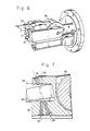
- FIG. 6 is a fragmentary perspective view of a portion of the sector magnet assembly; and
- FIG. 7 is a sectional view of a portion of the sector magnet assembly.
- A schematic-type elevational drawing of an MIBL system contemplated by the present invention is shown in FIG. 1. The system features a compact, vertical ion beam column approximately 1.7 meters in total length, which is considerably smaller than prior ion implantation accelerators used for MIBL applications. The system is capable of producing an H+ ion beam with energies up to 300keV and current densities up to 5J..lA/cm2.
- The MIBL optical column includes a surrounding vacuum enclosure, indicated by
reference 2, which provides mechanical support for the various components of the system. For purposes of simplification, details of the vacuum enclosure are not shown, nor are cooling systems for some of the components or the details of electrical leads. These items are conventional in nature, and can be implemented as desired. - A high efficiency H+ ion source 4 is located at the top of the column. The ion source is of the arc- discharge type with magnetic multiple confinement. This type of device achieves high source efficiency by providing long confinement times for ionizing electrons, while maintaining a major portion of the plasma in an essentially field-free (less than 0.002T (20 Gauss)) region. Such field-free regions are occupied by uniform, quiescent plasmas with low effective plasma temperatures suitable for extracting high optical quality ion beams. A small (less than 5mm (0.2")), slowly diverging (less than 15 mrad) beam is extracted from the source by a two-
stage extraction mechanism 6.Extractor 6, described in more detail below, regulates the extracted current level by the field in its first stage, and controls the extracted beam divergence predominantly by the field in its second stage. - After receiving its initial acceleration from
extractor 6, the beam is directed to a variable field sector electromagnet 8, which causes the various particles within the beam to be angularly deflected by amounts that vary in proportion to the mass of each particle. The magnet is specially designed so that H+ ions within the beam are deflected to a desiredbeam path 10, while heavier ions are deflected by lesser amounts and thereby eliminated from the beam. The magnet is further designed to preserve a high quality virtual point source for the beam, which is important in the further manipulation of the beam within the optical column, and also keeps the cross-section of the beam generally circular. The removal of higher mass ions and neutral beam components is necessary to control the resist exposure dose, and to reduce mask heating effects. - Sector magnet 8 is positioned within the optical column at a location at which the beam has received an initial acceleration but prior to full acceleration to the final desired energy level, since the required magnetic fields at the lower energy location are considerably less. The magnet structure can thus be made more compact than would be the case for a magnet capable of handling H+ ions with energies up to 300keV. Furthermore, the elimination of heavier particles prior to full acceleration reduces the electrical load on the high voltage supplies, and eliminates the radiation background produced by stopping high energy ions. The sector magnet is carefully designed so that the beam is matched to the optics of the acceleration stages, described below.
- After processing by the sector magnet, the essentially pure H+ beam is passed through the central aperture of a
plate 12 to limit stray ions. The radius of the beam at the aperture is limited to about 0.15cm., and its angular divergence is limited to 10mrad. An octupole deflector 13 is positioned belowaperture plate 12 to provide a mechanism for performing fine adjustments in the alignment of the mass analyzed beam with the optical axis of the column, and in the shape of the beam. This deflector can also be used in effect to periodically turn the beam "off" during the wafer stepping and alignment periods when the MIBL system is used in a high throughput mode. The beam is turned "on" only during those periods when actual resist exposure is desired, typically about 0.5 second out of a total 1.5 second step-align-expose cycle. Applying an appropriate voltage to octupole 13 deflects the beam out of the column path, in effect "blanking" the beam. While a lesser number of electrodes could be used to accomplish this periodic blanking, an octupole is preferred because the same device can be used to align and shape the beam. A DC voltage is applied to the octupole for the aligning and shaping function, with a much higher voltage super-imposed to control beam "blanking". - Upon emerging from
aperture plate 12 and octupole 13 the beam is processed by a pair ofdual cylinder lenses 14 and 16. Such lenses have the advantage of having constant optical properties when accelerating the beam by a fixed multiple of its energy at the entrance to the lens. The first lens 14 comprises a pair ofhollow cylinders 18 and 20, between which a voltage differential is established to focus the beam at an angle of convergence which is at least three times its angular divergence upon entering the lens. Thesecond lens 16 consists of another pair ofhollow cylinders second lens 16, so that the beam is highly collimated when it emerges fromlens 16. With appropriate applied voltage differentials, each lens increases the beam energy by a factor of 5 for a total energy multiplication of 25 (the increase in beam energy by each lens is equal to the ratio of its exit voltage over its entrance voltage, all relative to the ion source voltage). - The beam crossover point is mechanically limited by an
aperture plate 26 on which current can be monitored to control a final adjustment of the first lens 14, fixing its demagnified image at the focal point of the second lens. From the crossover point, the beam expands at an amplified angular divergence compared to its initial divergence until it reaches the principle plane of thesecond lens 16. At the second lens the H+ ions are collimated into a substantially parallel beam, with a divergence of less than 2mrad and a diameter of 1.7cm or greater. Thus, the use of the demagnifying first lens 14 enables the achievement of a small geometry in the ion source/magnet region by initially generating a small, low divergence beam and then expanding the beam in the first lens acceleration stage to obtain the final beam dimensions. At the same time, theaperture plate 26 at the beam crossover point ensures proper beam optics upon entry to the second lens, while discriminating against any neutral beam components which may have formed between magnet 8 and the first lens 14. - The overall length of the optical column from the entrance of the first lens to the exit of the second lens is approximately one meter. With a maximum applied voltage of 300kV, the lenses are thus contained within substantially the maximum lengths over which the maximum column voltage can be isolated by the atmospheric side of the insulating
vacuum walls 2. These walls consist of a series of ceramic insulators capable of isolating a total of 300kV, while providing vacuum-tight seals to a level of 10-3Pa or less. The insulators are joined by means of bonded metal flanges which match the insulator expansion coefficient and are also used to support and align the lens elements. To optimize the resistance of the insulators to voltage breakdown, shadow rings made from insulating polymeric material are used to increase the insulator surface path and to support corona shields with a radius of 15cm (6") or more around the mated flanges. - Another
apertured plate 28 positioned immediately below thesecond lens 16 has a large aperture designed to conform the shape of the beam to the mask opening. Below this aperture plate anotheroctupole deflector 30 is positioned in the beam path to steer the beam into alignment with channeling axis of the underlying mask. The mask is generally formed from a single crystal silicon membrane, characterized by periodic "channels" through which the beam can pass with minimum scatter, absorption and energy loss. An octupole deflector is preferred because it provides x-y deflection combinations in a very compact package. To steer a 300keV H+ ion beam with a diameter of 2.3cm by ±1°,the octupole has a 10cm. bore and 20cm. long electrodes, with biases of ±2500 volts or less. The octupole power supply preferably regulates the biases applied to the octupole to within 0.1%, corresponding to a beam tilt angle of less than 0.025 mrad, and programs the voltages with an accuracy of 1% of full scale. The alignment position is determined by peaking of the transmitted proton flux, which is monitored by a Faraday cup placed behind the mask. - The beam steering capability provided by
octupole deflector 30 enables a convenient adjustment of the beam path to maintain a proper angular orientation between the beam and the channeling mask. This replaces the cumbersome prior technique which required a tilting of not only the mask but the wafer and its support stage to maintain the necessary angular alignment. With the present invention the mask position can be fixed. - A
mask 32 is positioned in the beam path belowoctupole deflector 30. The mask positioning mechanism includes anautomatic alignment system 34 such as that disclosed in U.S. Patent Application Serial No. 590,135, (now US-A-4 596 467), filed March 16,1984 by John L. Bartelt, one of the present inventors and having a common assignee with this application (see also EP-A-174935). The system detects alignment marks on the mask and actuates a positioning adjustment mechanism to maintain proper alignment. Asemiconductor wafer substrate 36 is supported on awafer platform 37 below the mask. The shaped and collimated ion beam passes through the mask to expose a resist on the wafer, except for the areas delineated by the mask pattern. Thewafer platform 37 is equipped with an appropriate mechanism to effect step and repeat movements, as known, in the art, for replicating the mask pattern on the substrate. It is important to note that the tilt of the ion beam produced by the octupole deflector 30 to align the beam with the possibly non-normal mask- channeling axis can cause an apparent image shift with respect to the mask-wafer alignment apparatus. This shift is corrected in real time by feeding the octupole deflection voltages into the mask-wafer alignment electronics. A wafer position change is thus produced that compensates for the ion beam shift. - A
variable power supply 38 provides the necessary voltages to the various stages of the acceleration column. To maintain beam stability and uniformity, a power supply having regulation and ripple of not more than 0.1 % should be used. If more stringent stabilization is necessary, closed feedback control loops can be inserted to control parameters such as the current level of the initial beam, or the beam energy after passage through the sector magnet. In general, the beam current intensity should be maintained to within 10% of a predetermined value. - The
power supply 38 provides a DC voltage in the range of 200-300kV to theion source 4, a voltage in the range of 192-288kV to theextraction electrodes 6,aperture plate 12 and the entrance cylinder 18 of the first lens, and a voltage in the range of 160-240kV to the firstlens exit cylinder 20,aperture plate 26 and the secondlens entrance cylinder 22; the secondlens exit cylinder 24 is grounded. All of the voltage outputs from the power supply vary together, so that all of the voltage outputs are at similar points within their respective ranges at any given time. - It can be seen that, taking the ion source voltage as a reference, the ratio of the voltages applied to the exit and entry cylinders of the first lens 14 is 5:1, and the ratio of the voltages applied to the exit and entrance cylinders of the
second lens 16 is likewise 5:1. Specifically, if the various voltage outputs frompower supply 38 are in the middle of their ranges, the voltage at theextraction electrode 6 and at the first lens entrance cylinder 18 relative to the ion source will be -10kV, the voltage at the firstlens exit cylinder 20 and the secondlens entrance cylinder 22 will be -50kV, and the voltage at the secondlens exit cylinder 24 will be -250kV. Since the outputs frompower supply 38 vary in tandem with each other, a simple adjustment of the power supply can be used to alter the beam power, while maintaining the voltage ratios across the two lenses at 5:1 to preserve the beam dimensions. - Details of the preferred H+ ion source are shown in FIGS. 2 and 3. H2 gas is bled into an
arc chamber 40, in which electrons from atungsten filament 42 ionize the gas to produce a plasma discharge. Rare earth (Sm-Co)permanent magnets 44 are mounted in an octupole configuration centered about the cylindrical axis of the arc chamber to confine the plasma toward the center of the chamber. The magnet fields increase the electron pathlengths, causing more electron-ion collisions within the plasma, and enhancing the conversion of H2 to H+. The magnetic field outside the chamber is clamped bymild steel yokes 46 connecting neighboring magnet pairs. Aclamp 48 is provided within each yoke to hold it in place with respect to the arc chamber. To protect the magnets from overheating and a subsequent loss of field strength due to the discharge power, the arc chamber is cooled by a forced Freon flow through anorifice 50 in the chamber backplate 52. - Inside the arc chamber the magnetic field intensity varies from about 0.15T (1.5kG) at the wall near a pole to less than 0.001T (10G) at the chamber axis. This configuration combines a high electron confinement at the anode walls, resulting in a high discharge efficiency, with a low field region (less than 0.002T (20G)) in which a quiescent plasma an be created. Electrons are confined at either end of the arc chamber by
graphite electrodes 54 biased at the cathode potential. This bias on the plasma confinement electrodes provides some initial collimation of the emitted ions prior to the influence of the extraction electrodes, discussed immediately below. -
Confinement electrode 54 is mounted on a boronnitride insulating fixture 56 which extends forward from the emission end of the arc chamber. Afirst extraction electrode 58 is held by the insulating fixture parallel to and spaced away from theconfinement electrode 54, while asecond extraction electrode 60 is held by the insulating fixture parallel to and spaced away fromfirst extraction electrode 58 on the opposite side thereof fromconfinement electrode 54. Each of the electrodes has a central aperture for the passage of an ion beam from within the arc chamber. - As an alternate to the ion source configuration shown in FIGS. 2 and 3, a set of annular magnets concentric with the arc chamber and polarized in the axial direction may be used. This arrangement provides a somewhat larger field-free region, but has lower overall efficiency due to lower magnetic field strengths at the chamber wall, resulting in higher electron losses. The larger field-free region, however, would permit the extraction of larger area beams if desired.
- Details of the extraction mechanism used to obtain an ion beam with a virtual point source are shown in FIG. 4. The dimensions, relative positions and voltages applied to the electrodes are designed to produce an ion beam with a desired size and angular divergence. The orientation of the electrodes in FIG. 4 is a mirror image of the representation shown in FIG. 2.
Confinement electrode 54 is about 0.25mm thick, with a 0.25mm diameter aperture 62 which flares outwardly away from its axis at an angle of 67°. The voltage potential ofelectrode 54 may be taken as a zero reference for purposes of comparison with the voltages applied to the other electrodes. - The
first extraction electrode 58 is spaced about 5mm fromelectrode 54, and is 0.5mm thick with a 0.25mm diameter aperture 64, and a nominal applied voltage of -2kV with respect to the voltage onelectrode 54. - The
second extraction electrode 60 actually consists of a pair ofparallel electrodes electrode 66 is spaced 10mm from the center of thefirst extraction electrode 58, and has a thickness of 1 mm.Electrode 68, the center of which is spaced 2mm from the center ofelectrode 66 on the other side fromelectrode 58, is 0.5mm thick. Therespective apertures electrodes electrodes electrodes Electrode 60 is implemented in a dual parallel electrode configuration with the first electrode having a slightly higher voltage to prevent the downstream electrons from entering the discharge chamber. - The nominal voltages applied to the various electrodes can be adjusted by up to ±20% to control the output energy of the beam. With the configuration shown, H+ beams of 8 to 12keV can be produced with current and collimation constant to within ±10%. In conjunction with the two accelerating lenses in the column design, this energy range corresponds to a final-beam energy of 200-300keV.
- For improved collimation of the extracted beam, the electric field strength in the first gap between
electrodes electrodes plasma confinement electrode 54 at the source cathode potential, which in FIG. 4 is taken as a zero reference. The small diameter ofaperture 62 inconfinement electrode 54 provides a very low neutral gas flow from the ion source. As a result, the H2 gas experiences a long residence time in the discharge chamber, enhancing the probability of H+ ion generation. Furthermore, the low gas load permits background pressures of less than 1.33 x 10⁻³ Pa (10-5 Torr) to be maintained in the ion source region while vacuum pumping only from the low voltage end of the column in the region of thesecond lens 16. Thus, the loss of beam current due to charge exchange processes is reduced and voltage isolation conditions are preserved without the need for a separate high voltage vacuum system or a cumbersome differential pumping scheme. The beam extraction mechanism of FIG. 4 has been used to produce beams of 15-20uA at 10keV with angular divergences of 10-12 mrad at background pressures of less than 6.67 x 10⁻⁴ Pa (5 x 10⁻⁶ Torr). - The preferred design of the variable field sector electromagnet 8 is shown in FIG. 5. The expanding beam 74 which emerges from the extraction electrodes generally includes undesired particles, such as H atoms and molecules, metal impurity ions resulting from sputtering inside the ion source, and sometimes ions from impurity gases. The magnet 8 angularly deflects the paths of the various particles within the beam. The amount by which each particle is deflected varies in inverse proportion to its mass, and the magnet is specially designed so that substantially only H+ ions are transmitted along a desired
path 76 corresponding to the axis of the MIBL column. The action of the magnet is to deflect H+ ions into alignment with designedpath 76 without substantially changing its cylindrical symmetry. Thus, the H+ beam 78 emerging from the magnet is characterized by a virtual point source, which is important for the later processing of the beam bylenses 14 and 16. Heavier particles, such asbeam 80 comprised of H'2, are deflected by lesser amounts and are blocked byaperture plate 12. - The primary characteristics of magnet 8 are illustrated in FIG. 5. A 20° sector electromagnet is used with a 1.5cm pole gap and flat, tilted pole faces. The entrance and exit pole face tilt angles are +8.2° and +5.5°, respectively. For an incident beam energy of 10kev and a field of 0.1T (1kG), the magnet has a mass resolution of greater or equal to 3.2, and produces a symmetric beam which appears to originate from a
point source 82 located 12.9cm behindaperture plate 12. - The magnet pole structure is illustrated in FIG. 6. An
iron yoke 84 supports and provides a magnetic coupling between aniron core 86 about which a conductive coil (not shown) is wrapped, and one of themagnetic pole pieces 88. An opposedmagnetic pole piece 90 and the opposite end ofcore 86 are supported and magnetically coupled together by a second iron yoke (not shown). The ion beam passes between the two pole pieces, and is deflected by the magnetic field therebetween. - It is important that the ion source/extractor mechanism be accurately fixed or positionally adjusted with respect to the magnet and to the column lens assembly. In general, the mechanical alignment accuracy should be less than 10% of the beam diameter. Mounting structures are preferably provided for both the ion source and magnet assembly which provide fine x, y and angular adjustments. A portion of the magnet mounting structure which is intended to facilitate alignment with the ion source is shown in FIG. 7. The
support structure 92 which holdsyoke 84 in place includes anentrance port 94 which admits the ion beam from the source and extractor electrodes, anexit port 96 which transmits the deflected H+ beam emerging from the magnet, and an alignment port 98 which is coaxial withentrance port 94 on the opposite side of the magnet. Asecond alignment port 100 is formed on the opposite side of the magnet from, and coaxial with,exit port 96. The magnet assembly is aligned to the MIBL column axis using a laser beam directed along the axis ofports apertures 94 and 98. The small physical dimensions of the source and magnet permit the complete assembly, which comprises the high voltage section of the MIBL system, to be packaged in a very compact geometry. - Referring back to FIG. 1, after the H+ beam has passed through the magnet it arrives at the first lens 14, which increases the angular expansion of the beam by a factor greater than 3 beyond the beam crossover point at
aperture plate 26. Beyondaperture plate 26 the beam expands as it drifts approximately 27cm. along the column axis, until it reaches the principal plane of thesecond lens 16. Here the H+ ions are collimated into a parallel beam with a divergence of less than 2mrad and a diameter of 1.7cm or more. The H+ ions emerge from the lens with a final energy of 200-300keV, depending upon the setting of the power supply. After emerging fromlens 16, the beam is apertured byplate 28 to about 1.5cm diameter to eliminate any non-uniformities in the fringes of the beam profile prior to its entrance intooctupole deflector 30. Inoctupole deflector 30 the beam is steered into alignment with the channeling axis ofmask 32. - An MIBL system and method has thus been shown and described which offers considerable advantages over the prior art. It is much more compact than alternate systems, thereby reducing the costs associated with semiconductor fabrication clean rooms, lessening the possibility of beam deflection by external magnetic fields, and reducing vacuum pumping requirements. The described system provides all of the performance capabilities necessary for MIBL within a package that is 4-5 times smaller and much more energy efficient than typical ion implantation accelerators, and is comparable in size to an electron beam exposure column. It is believed to be the most compact of any ion beam exposure system with a similar range of beam energy and size requirements, and is considerably less expensive than ion implantation devices. As numerous variations and alternate embodiments will occur to those skilled in the art, it is intended that the invention be limited only in terms of the appended claims.
Claims (26)
Priority Applications (1)
| Application Number | Priority Date | Filing Date | Title |
|---|---|---|---|
| AT87901780T ATE56308T1 (en) | 1986-03-07 | 1987-01-27 | SYSTEM AND PROCESS OF MASKED ION BEAM LITHOGRAPHY. |
Applications Claiming Priority (2)
| Application Number | Priority Date | Filing Date | Title |
|---|---|---|---|
| US06/837,127 US4757208A (en) | 1986-03-07 | 1986-03-07 | Masked ion beam lithography system and method |
| US837127 | 1986-03-07 |
Publications (2)
| Publication Number | Publication Date |
|---|---|
| EP0258383A1 EP0258383A1 (en) | 1988-03-09 |
| EP0258383B1 true EP0258383B1 (en) | 1990-09-05 |
Family
ID=25273592
Family Applications (1)
| Application Number | Title | Priority Date | Filing Date |
|---|---|---|---|
| EP87901780A Expired - Lifetime EP0258383B1 (en) | 1986-03-07 | 1987-01-27 | Masked ion beam lithography system and method |
Country Status (6)
| Country | Link |
|---|---|
| US (1) | US4757208A (en) |
| EP (1) | EP0258383B1 (en) |
| JP (1) | JPH0799683B2 (en) |
| KR (1) | KR900008793B1 (en) |
| DE (1) | DE3764747D1 (en) |
| WO (1) | WO1987005438A1 (en) |
Families Citing this family (36)
| Publication number | Priority date | Publication date | Assignee | Title |
|---|---|---|---|---|
| AT393333B (en) * | 1986-11-27 | 1991-09-25 | Ims Ionen Mikrofab Syst | ION PROJECTION DEVICE FOR SHADOW PROJECTION |
| AT391771B (en) * | 1987-03-05 | 1990-11-26 | Ims Ionen Mikrofab Syst | DEVICE FOR REDUCING OR 1: 1 ION PROJECTION LITHOGRAPHY |
| GB2216714B (en) * | 1988-03-11 | 1992-10-14 | Ulvac Corp | Ion implanter system |
| US4929839A (en) * | 1988-10-11 | 1990-05-29 | Microbeam Inc. | Focused ion beam column |
| GB2233124B (en) * | 1989-06-06 | 1994-02-09 | Mitsubishi Electric Corp | Ion implantation apparatus |
| US5155357A (en) * | 1990-07-23 | 1992-10-13 | Massachusetts Institute Of Technology | Portable mass spectrometer |
| US5130552A (en) * | 1990-12-17 | 1992-07-14 | Applied Materials, Inc. | Improved ion implantation using a variable mass resolving system |
| CA2106598A1 (en) * | 1991-03-25 | 1992-09-26 | Philip James Martin | Arc source macroparticle filter |
| AU655009B2 (en) * | 1991-03-25 | 1994-12-01 | Commonwealth Scientific And Industrial Research Organisation | Arc source macroparticle filter |
| EP0564438A1 (en) * | 1992-03-30 | 1993-10-06 | IMS Ionen Mikrofabrikations Systeme Gesellschaft m.b.H. | Particle imaging system, in particular ion optical imaging system |
| JPH08274020A (en) * | 1995-02-13 | 1996-10-18 | Ims Ionen Mikrofab Syst Gmbh | Projection lithography system using charged particles |
| US5563418A (en) * | 1995-02-17 | 1996-10-08 | Regents, University Of California | Broad beam ion implanter |
| EP0732624B1 (en) * | 1995-03-17 | 2001-10-10 | Ebara Corporation | Fabrication method with energy beam |
| US5611870A (en) * | 1995-04-18 | 1997-03-18 | Edtek, Inc. | Filter array for modifying radiant thermal energy |
| DE19734059B4 (en) * | 1996-08-20 | 2007-01-11 | Ims-Ionen Mikrofabrikations Systeme Ges.M.B.H. | Arrangement of shadows throw lithography |
| SG52858A1 (en) * | 1996-11-07 | 1998-09-28 | Univ Singapore | Micromachining using high energy light ions |
| US6888146B1 (en) * | 1998-04-10 | 2005-05-03 | The Regents Of The University Of California | Maskless micro-ion-beam reduction lithography system |
| GB2345574A (en) * | 1999-01-05 | 2000-07-12 | Applied Materials Inc | Apparatus and method for monitoring and tuning an ion beam in an ion implantation apparatus |
| US6472673B1 (en) * | 1999-07-29 | 2002-10-29 | Ims Ionen-Mikrofabrikations Systeme Gmbh | Lithographic method for producing an exposure pattern on a substrate |
| US6693289B1 (en) | 2000-02-07 | 2004-02-17 | Nec Electronics, Inc. | Operationally positionable source magnet field |
| EP1171901B1 (en) * | 2000-02-09 | 2008-10-08 | Fei Company | Multi-column fib for nanofabrication applications |
| US6794660B2 (en) * | 2000-10-31 | 2004-09-21 | Nikon Corporation | Long stroke mover for a stage assembly |
| AU2002247083A1 (en) * | 2001-02-06 | 2002-08-19 | Proteros, Llc | System and method for amplifying an angle of divergence of a scanned ion beam |
| EP1883094B1 (en) * | 2006-07-24 | 2012-05-02 | ICT, Integrated Circuit Testing Gesellschaft für Halbleiterprüftechnik mbH | Charged particle beam device and method for inspecting specimen |
| US7476855B2 (en) * | 2006-09-19 | 2009-01-13 | Axcelis Technologies, Inc. | Beam tuning with automatic magnet pole rotation for ion implanters |
| WO2008140585A1 (en) | 2006-11-22 | 2008-11-20 | Nexgen Semi Holding, Inc. | Apparatus and method for conformal mask manufacturing |
| US10991545B2 (en) | 2008-06-30 | 2021-04-27 | Nexgen Semi Holding, Inc. | Method and device for spatial charged particle bunching |
| US10566169B1 (en) | 2008-06-30 | 2020-02-18 | Nexgen Semi Holding, Inc. | Method and device for spatial charged particle bunching |
| US9040867B2 (en) * | 2012-12-21 | 2015-05-26 | United Technologies Corporation | Manufacturing machine with magnetic field beam steering |
| JP6076838B2 (en) | 2013-05-31 | 2017-02-08 | 住友重機械イオンテクノロジー株式会社 | Insulation structure and insulation method |
| JP6030099B2 (en) * | 2014-08-18 | 2016-11-24 | 東京エレクトロン株式会社 | Residual layer removal method and residual layer removal apparatus |
| US11049691B2 (en) * | 2017-12-21 | 2021-06-29 | Varian Semiconductor Equipment Associates, Inc. | Ion beam quality control using a movable mass resolving device |
| US11715622B2 (en) | 2020-08-05 | 2023-08-01 | Kla Corporation | Material recovery systems for optical components |
| US20240393696A1 (en) * | 2021-03-31 | 2024-11-28 | The Regents Of The University Of California | Uv lithography system and method |
| US11574796B1 (en) | 2021-07-21 | 2023-02-07 | Applied Materials, Inc. | Dual XY variable aperture in an ion implantation system |
| US12493005B1 (en) | 2022-06-07 | 2025-12-09 | Nexgen Semi Holding, Inc. | Extended range active illumination imager |
Family Cites Families (11)
| Publication number | Priority date | Publication date | Assignee | Title |
|---|---|---|---|---|
| US3845312A (en) * | 1972-07-13 | 1974-10-29 | Texas Instruments Inc | Particle accelerator producing a uniformly expanded particle beam of uniform cross-sectioned density |
| US3913320A (en) * | 1974-11-13 | 1975-10-21 | Ion Tech Inc | Electron-bombardment ion sources |
| JPS51148370A (en) * | 1975-06-14 | 1976-12-20 | Fujitsu Ltd | Electron ray exposure method |
| DE2547079C3 (en) * | 1975-10-17 | 1979-12-06 | Siemens Ag, 1000 Berlin Und 8000 Muenchen | Process for corpuscular irradiation of a specimen |
| US4013891A (en) * | 1975-12-15 | 1977-03-22 | Ibm Corporation | Method for varying the diameter of a beam of charged particles |
| JPS5361280A (en) * | 1976-11-12 | 1978-06-01 | Hitachi Ltd | Pattern projector |
| US4142132A (en) * | 1977-07-05 | 1979-02-27 | Control Data Corporation | Method and means for dynamic correction of electrostatic deflector for electron beam tube |
| US4158141A (en) * | 1978-06-21 | 1979-06-12 | Hughes Aircraft Company | Process for channeling ion beams |
| US4310743A (en) * | 1979-09-24 | 1982-01-12 | Hughes Aircraft Company | Ion beam lithography process and apparatus using step-and-repeat exposure |
| US4383180A (en) * | 1981-05-18 | 1983-05-10 | Varian Associates, Inc. | Particle beam accelerator |
| JPS5877230A (en) * | 1981-11-04 | 1983-05-10 | Hitachi Ltd | Pattern formation |
-
1986
- 1986-03-07 US US06/837,127 patent/US4757208A/en not_active Expired - Lifetime
-
1987
- 1987-01-27 WO PCT/US1987/000106 patent/WO1987005438A1/en not_active Ceased
- 1987-01-27 KR KR1019870701019A patent/KR900008793B1/en not_active Expired
- 1987-01-27 EP EP87901780A patent/EP0258383B1/en not_active Expired - Lifetime
- 1987-01-27 JP JP62501440A patent/JPH0799683B2/en not_active Expired - Lifetime
- 1987-01-27 DE DE8787901780T patent/DE3764747D1/en not_active Expired - Fee Related
Also Published As
| Publication number | Publication date |
|---|---|
| DE3764747D1 (en) | 1990-10-11 |
| KR880701453A (en) | 1988-07-27 |
| WO1987005438A1 (en) | 1987-09-11 |
| KR900008793B1 (en) | 1990-11-29 |
| JPH0799683B2 (en) | 1995-10-25 |
| US4757208A (en) | 1988-07-12 |
| JPS63502707A (en) | 1988-10-06 |
| EP0258383A1 (en) | 1988-03-09 |
Similar Documents
| Publication | Publication Date | Title |
|---|---|---|
| US4757208A (en) | Masked ion beam lithography system and method | |
| US5206516A (en) | Low energy, steered ion beam deposition system having high current at low pressure | |
| US6924493B1 (en) | Ion beam lithography system | |
| US6768120B2 (en) | Focused electron and ion beam systems | |
| US6130436A (en) | Acceleration and analysis architecture for ion implanter | |
| US10840054B2 (en) | Charged-particle source and method for cleaning a charged-particle source using back-sputtering | |
| TWI416572B (en) | Multi-purpose ion implanter beam stream configuration | |
| US4661712A (en) | Apparatus for scanning a high current ion beam with a constant angle of incidence | |
| US4514638A (en) | Electron-optical system with variable-shaped beam for generating and measuring microstructures | |
| US4687940A (en) | Hybrid focused-flood ion beam system and method | |
| US20240170248A1 (en) | Particle beam system | |
| WO1998033199A2 (en) | Ion accelerator for use in ion implanter | |
| JP3350374B2 (en) | Focused ion beam apparatus, processing method and semiconductor device manufacturing method | |
| EP3518268B1 (en) | Charged-particle source and method for cleaning a charged-particle source using back-sputtering | |
| JP2002110080A (en) | Ion implanter, its waveguide, mass spectrometer, and method of delivering microwave power to the device | |
| US6486480B1 (en) | Plasma formed ion beam projection lithography system | |
| US6888146B1 (en) | Maskless micro-ion-beam reduction lithography system | |
| US6897457B1 (en) | Apparatus and method for monitoring and tuning an ion beam in ion implantation apparatus | |
| US20040051053A1 (en) | Universal pattern generator with multiplex addressing | |
| EP0079931B1 (en) | Focused ion beam microfabrication column | |
| EP0809857B1 (en) | Generator of ribbon-shaped ion beam | |
| EP0995214B1 (en) | Method and apparatus for neutralising space charge in an ion beam | |
| JP2002175771A (en) | Ion implanting equipment | |
| Spädtke | Beam formation and transport | |
| JPS61234033A (en) | Impurity introduction method to semiconductor substrate |
Legal Events
| Date | Code | Title | Description |
|---|---|---|---|
| PUAI | Public reference made under article 153(3) epc to a published international application that has entered the european phase |
Free format text: ORIGINAL CODE: 0009012 |
|
| 17P | Request for examination filed |
Effective date: 19871104 |
|
| AK | Designated contracting states |
Kind code of ref document: A1 Designated state(s): AT DE FR GB NL |
|
| RIN1 | Information on inventor provided before grant (corrected) |
Inventor name: SLAYMAN, CHARLES, W. Inventor name: WARD, J., WILLIAM Inventor name: OLNEY, ROSS, D. Inventor name: BARTELT, JOHN, L. Inventor name: WOOD, JAMES, E. Inventor name: MCKENNA, CHARLES, M. |
|
| 17Q | First examination report despatched |
Effective date: 19890302 |
|
| GRAA | (expected) grant |
Free format text: ORIGINAL CODE: 0009210 |
|
| AK | Designated contracting states |
Kind code of ref document: B1 Designated state(s): AT DE FR GB NL |
|
| REF | Corresponds to: |
Ref document number: 56308 Country of ref document: AT Date of ref document: 19900915 Kind code of ref document: T |
|
| ET | Fr: translation filed | ||
| REF | Corresponds to: |
Ref document number: 3764747 Country of ref document: DE Date of ref document: 19901011 |
|
| PLBE | No opposition filed within time limit |
Free format text: ORIGINAL CODE: 0009261 |
|
| STAA | Information on the status of an ep patent application or granted ep patent |
Free format text: STATUS: NO OPPOSITION FILED WITHIN TIME LIMIT |
|
| 26N | No opposition filed | ||
| PGFP | Annual fee paid to national office [announced via postgrant information from national office to epo] |
Ref country code: FR Payment date: 19931208 Year of fee payment: 8 |
|
| PGFP | Annual fee paid to national office [announced via postgrant information from national office to epo] |
Ref country code: GB Payment date: 19931210 Year of fee payment: 8 |
|
| PGFP | Annual fee paid to national office [announced via postgrant information from national office to epo] |
Ref country code: AT Payment date: 19931213 Year of fee payment: 8 |
|
| PGFP | Annual fee paid to national office [announced via postgrant information from national office to epo] |
Ref country code: DE Payment date: 19931217 Year of fee payment: 8 |
|
| PGFP | Annual fee paid to national office [announced via postgrant information from national office to epo] |
Ref country code: NL Payment date: 19940131 Year of fee payment: 8 |
|
| PG25 | Lapsed in a contracting state [announced via postgrant information from national office to epo] |
Ref country code: GB Effective date: 19950127 Ref country code: AT Effective date: 19950127 |
|
| PG25 | Lapsed in a contracting state [announced via postgrant information from national office to epo] |
Ref country code: NL Effective date: 19950801 |
|
| GBPC | Gb: european patent ceased through non-payment of renewal fee |
Effective date: 19950127 |
|
| PG25 | Lapsed in a contracting state [announced via postgrant information from national office to epo] |
Ref country code: FR Effective date: 19950929 |
|
| NLV4 | Nl: lapsed or anulled due to non-payment of the annual fee |
Effective date: 19950801 |
|
| PG25 | Lapsed in a contracting state [announced via postgrant information from national office to epo] |
Ref country code: DE Effective date: 19951003 |
|
| REG | Reference to a national code |
Ref country code: FR Ref legal event code: ST |