EP0257954A2 - Oxygen sensing pacemaker - Google Patents
Oxygen sensing pacemaker Download PDFInfo
- Publication number
- EP0257954A2 EP0257954A2 EP19870307263 EP87307263A EP0257954A2 EP 0257954 A2 EP0257954 A2 EP 0257954A2 EP 19870307263 EP19870307263 EP 19870307263 EP 87307263 A EP87307263 A EP 87307263A EP 0257954 A2 EP0257954 A2 EP 0257954A2
- Authority
- EP
- European Patent Office
- Prior art keywords
- light
- coupled
- proximal end
- generating
- proximal
- Prior art date
- Legal status (The legal status is an assumption and is not a legal conclusion. Google has not performed a legal analysis and makes no representation as to the accuracy of the status listed.)
- Granted
Links
Images


Classifications
-
- A—HUMAN NECESSITIES
- A61—MEDICAL OR VETERINARY SCIENCE; HYGIENE
- A61N—ELECTROTHERAPY; MAGNETOTHERAPY; RADIATION THERAPY; ULTRASOUND THERAPY
- A61N1/00—Electrotherapy; Circuits therefor
- A61N1/02—Details
- A61N1/04—Electrodes
- A61N1/05—Electrodes for implantation or insertion into the body, e.g. heart electrode
- A61N1/056—Transvascular endocardial electrode systems
-
- A—HUMAN NECESSITIES
- A61—MEDICAL OR VETERINARY SCIENCE; HYGIENE
- A61N—ELECTROTHERAPY; MAGNETOTHERAPY; RADIATION THERAPY; ULTRASOUND THERAPY
- A61N1/00—Electrotherapy; Circuits therefor
- A61N1/18—Applying electric currents by contact electrodes
- A61N1/32—Applying electric currents by contact electrodes alternating or intermittent currents
- A61N1/36—Applying electric currents by contact electrodes alternating or intermittent currents for stimulation
- A61N1/362—Heart stimulators
- A61N1/365—Heart stimulators controlled by a physiological parameter, e.g. heart potential
- A61N1/36514—Heart stimulators controlled by a physiological parameter, e.g. heart potential controlled by a physiological quantity other than heart potential, e.g. blood pressure
- A61N1/36557—Heart stimulators controlled by a physiological parameter, e.g. heart potential controlled by a physiological quantity other than heart potential, e.g. blood pressure controlled by chemical substances in blood
Definitions
- the present invention relates generally to medical devices and more specifically relates to implantable electronic devices for muscle stimulation.
- pacemakers As an alternative to regulating pacing rate by sensing the contractions of the heart, some pacemakers have regulated rate in response to measurement of some other, physiological parameter.
- pacemakers proposed which vary rate in response to instantaneous blood pressure within the right atrium, as in U.S. Patent No. 3,358,690, in response to respiration as in U.S. Patent No. 3,593,718, in response to physical activity as in U.S. Patent No. 4,140,132 or in response to neurological activity as in U.S. Patent No. 4,210,219.
- the most promising techniques appear to involve varying of pacing rate in response to sensing of chemical parameters of the blood.
- the present invention comprises an improved oxygen sensor and associated circuitry for use within a cardiac pacemaker of the type in which pacing rate is dependent upon the percentage of oxygen saturation of the intracardiac venous blood.
- the preferred embodiment includes a hermetically sealed sensor capsule containing a two wavelength reflectance oximeter.
- the method of construction of this capsule assures its suitability for long term human implant.
- the invention includes timing, processing and output circuitry for operating the sensor in a predetermined time relationship with pacing output pulses and which allows the construction of a long term implantable lead which performs EKG sensing, cardiac pacing and two wave length reflectance oximetry using only three conductors. Minimizing the number of conductors is believed particularly valuable in long term implantable devices, where experience has shown that electronic complexity is preferable to mechanical complexity.
- FIG. 1 is an illustration of a prior art rate adaptive demand pacemaker in which sensed oxygen saturation is used to regulate the pacing rate.
- FIG. 2 is a plan view of a pacing and oxygen sensing lead according to the present invention.
- FIG. 3 is a side sectional view of the sensor body, a subassembly of the sensor capsule.
- FIG. 4 is a side sectional view of the window assembly, a subassembly of the sensor capsule.
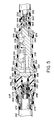
- FIG. 5 is a side sectional view through the completed sensor capsule.
- FIG. 6 is a top sectional view through the completed sensor capsule.
- FIG. 7 is a functional diagram of the sensor and associated circuitry.
- FIG. 8 is a schematic of the digital timing circuitry associated with the sensor capsule.
- FIG. 9 is a circuit diagram of the analog circuitry associated with the sensor.
- FIG. 10 is a timing diagram illustrating the operation of the sensor capsule, and its relation to the operation of the cardiac pacemaker with which it is intended to be employed.
- FIG. 1 illustrates a rate adaptive demand pacemaker in which sensed oxygen level is used to vary the escape interval of a demand pacemaker, as disclosed in U.S. Patent No. 4,467,807 issued to Bornzin. This figure is intended both to illustrate pertinent prior art in this area and to provide a general illustration of how the circuitry and sensor of the present invention may be functionally related to the circuitry of an implantable pacemaker.
- FIG. 1 shows a single chamber pacing system including a sensor 12 within the right ventricle 20 of heart 10, which generates a voltage on line 14 proportional to percentage of oxygen saturation in the right ventrical of the heart.
- the voltage on line 14 is processed by sensor processing circuitry 30 which includes an analog to digital converter which converts the voltage on line 14 to a binary number which is used to control the pacing rate set by demand logic 106 and fixed rate oscillator 112.
- Line 104 is coupled to an electrode in right ventricle 20 of the heart 10 and delivers electrical signals to the sense amplifier 102 which generates an output on line 108 indicative of the sensing of a natural contraction of the human heart. On sensing such a contraction, the timing period of the demand logic is reset.
- the incorporation of the present invention in an implantable pacemaker is discussed specifically with reference to the pacemaker disclosed in FIG. 1, the invention is believed equally applicable to other pacemakers employing alternate circuitry configurations for determining rate in response to an analog signal indicative of oxygen saturation.
- the invention would also be useful in conjunction with a pacemaker as disclosed in U.S. Patent No. 4,202,339 issued to Wirtzfeld, cited above.
- the invention may be used in asynchronous pacemakers, i.e. those without a demand function.
- FIG. 2 is a plan view of a permanently implantable lead according to the present invention.
- Lead 200 is provided with a pacing electrode 210 at its extreme distal tip, which is held in place within the heart by tines 212, which may be of the type described in U.S. Patent No. 3,902,501 issued to Citron et al or U.S. Patent No. 4,269,198 issued to Stokes.
- a sensor capsule 214 Located proximal to electrode 210 is a sensor capsule 214, which contains a two wavelength reflectance oximeter. Capsule 214 is spaced from electrode 210 by an insulative lead body 216 which encloses a conductor which couples electrode 210 to sensor capsule 214.
- Proximal to sensor 214 is an elongated lead body 218 which is preferably sheathed in a pliant, insulative material such as polyurethane or silicone rubber.
- Lead body 218 contains three coaxially mounted coiled conductors coupled to sensor capsule 214 and extended to connector assembly 220.
- Connector assembly 220 includes three connector surfaces 222, 224, and 226 which are coupled to the three conductors mounted within lead body 218.
- An anchoring sleeve 228 is optionally included to stabilize lead 200 at the point of venous insertion. Anchoring sleeve 228 may be of the type described in U.S. Patent No. 4,437,475 issued to White.
- FIG. 3 is a side sectional view of the sensor body assembly, a subassembly of the sensor capsule 214 of the present invention.
- the sensor body assembly includes a machined titanium sensor body 230, having longitudinal surface 231 which serves to mount the ceramic substrate 232 upon which the various electronic elements of the two frequency reflectance oximeter are located. These elements include a phototransistor 234, an infrared light emitting diode 236 and a red light emitting diode 238. Diodes 236 and 238 are separated from phototransistor 234 by a semicircular wall 240. At the proximal end of sensor body 230 is an aperture 242 in which a sapphire or glass feedthrough 246 is located.
- Feedthrough 246 has been brazed to sensor body 230 around its entire circumference, using a braze such as gold. Extending through and also brazed freedthrough 246 are two wires, of which only one, labeled 248, is visible in this view. Wire 248 is soldered to a conductive pad located on ceramic 232. At the distal end of sensor body 230 is a bore 250 which serves as a mounting point for a coiled conductor.
- FIG. 4 is a side sectional view of the window assembly of the sensor capsule.
- the window assembly includes an optically pure sapphire or glass tube 252 and two welding collars 254 and 256 located at the proximal and distal ends, respectively, of tube 252.
- Welding collars 254 and 256 are fabricated of titanium and are provided with circumferential indentations at their distal and proximal ends, respectively, which receive the ends of sapphire tube 252.
- Welding collars 254 and 256 are brazed to the proximal and distal ends of sapphire tube 252 around their entire circumference, using a braze which is preferably gold.
- the proximal and distal ends of tube 252 Prior to brazing, the proximal and distal ends of tube 252 are coated with a thin film of niobium or similar metalization to facilitate brazing. Vapor deposition or sputtering techniques may be used to provide this thin film.
- the capsule itself is assembled by sliding the window assembly of FIG. 4 proximally over the body assembly of FIG. 3, until the proximal end 258 of weld collar 254 is adjacent the shoulder 243 of sensor body 230 (FIG. 3)
- the inner diameter of the distal portion 260 of weld collar 256 is the same as the outer diameter of the distal portion 310 of sensor body 230.
- weld collar 254 and weld collar 256 may conveniently be laser welded to sensor body 230, around the circumference of proximal end 258 of weld collar 254 and of distal end 260 of weld collar 256.
- FIG. 5 is a side sectional view of the sensor capsule, mounted in the lead of FIG. 2.
- a coiled conductor 262 which is held in place by crimps 264 which mechanically and electrically couple it to sensor body 230.
- Conductor 262 extends to and is electrically coupled with tip electrode 210 (FIG. 2).
- Capsule adapter 268 is generally cylindrical and hollow in its construction, and includes a cross bore 270 for addition of backfill material 271.
- a capsule adapter 268 Welded to a capsule adapter 268 is a coiled conductor 272, which is coupled to connector pin 226 (FIG. 2).
- Located within the internal cavity 269 of adapter 268 are two, mutually insulated coaxially coiled conductors including coiled conductor 274 and coiled conductor 276, which are insulated by insulating sheaths 278 and 280, respectively.
- Conductor 276 is attached to wire 248, within a welding sleeve, not visible in this illustration.
- Conductor 274 is coupled to a second wire 247, passing through feedthrough 246.
- the entire lead is sheathed in an outer insulative sheath 282, which is preferably fabricated of polyurethane or other transparent, non-thrombogenic material.
- Cavity 269 is backfilled with epoxy 271. All other labeled elements correspond to identically numbered elements in FIGs. 3 and 4, above.
- FIG. 6 is a top cut away view of the sensor capsule mounted in the lead of FIG. 2.
- Conductors 274 and 276 are preferably multifilar coils which are welded to wires 247 and 248, and mounted within welding sleeves 284 and 286.
- wires 247 and 248 are coupled to two metallic pads 288 and 290 on substrate 232.
- Phototransistor 234 is seen to be mounted on a conductive pad 292, coupled to metallic pad 290.
- Phototransistor 234 is coupled by means of a fine wire 294 to a second conductive pad 296, coupled to metallic pad 288.
- Conductive pad 292 extends under wall 240, and serves as the mounting point for infrared LED 236.
- a third conductive pad 298 serves as a mounting point for red LED 238.
- LED's 236 and 238 are connected to pads 298 and 292 respectively, by means of fine wires 300 and 302.
- Conductive pad 298 is coupled to a fourth conductive pad 304 by means of a fine wire 306 and pad 304 is coupled to sensor body 230 by metallic strap 239. All other elements correspond to identically numbered elements in FIG. 3, 4 and 5.
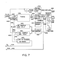
- FIG. 7 is a functional diagram of the sensor and its associated circuitry.
- the sensor hybrid 400 is illustrated schematically, showing the interconnection of infrared LED 236, red LED 238 and phototransistor 234.
- the three lines 402, 404 and 406 correspond to coiled conductors 272, 274 and 276, respectively, in FIGs. 5 and 6.
- Line 408 corresponds to conductor 262, shown in FIG. 5 and electrode 410 corresponds to tip electrode 210, shown in FIG. 2.
- the diode pair 236 and 238 is driven by a pair of push pull amplifiers 412 and 414.
- Amplifier 412 operates in a voltage output mode
- amplifier 414 operates in a current output mode.
- the returning current from phototransistor 234 is converted to a proportional DC voltage by the current mirror 416 and is delivered to the sample and hold switches 418 and 420 which recover the peak signal for each color.
- Pacing is accomplished by placing line 402 from voltage driver 412 at a logic 0 and placing line 458 to return amplifier 422 at a logic 1. For example, if the system employs a 3.6 volt lithium thionylchloride cell, this produces a pacing voltage of approximately 3.1 volts across the heart.
- Pacing return amplifier 422 is coupled to electrode 424, which may conveniently be the metal enclosure of the implanted pacemaker. Timing for the entire system is provided by integrated circuitry included in the timing block 246, which controls the timing and function of the pacing voltage driver 412 and the current driver 414 as well as determining times for operation of the sample and hold circuits 418 and 420.
- the outputs of sample and hold circuits 418 and 420 are coupled to a division network 428 which divides the output of IR sample and hold 420 on line 430 by the output of red sample and hold 418 on line 432 to produce a D.C. voltage signal on line 434 indicative of the percentage of oxygen saturation.
- IR/R division network 428 may be of the type illustrated in FIG. 1 of U.S. Patent No.
- Line 434 carrying an analog signal indicative of oxygen saturation may be coupled to the sensor processing circuitry of a pacemaker such as illustrated in FIG. 1.
- the sensor and associated circuitry may replace the sensor 12 and line 14 of FIG. 1, with the output of IR/R division network 428 functionally coupled to sensor processing circuitry 30.
- Timing circuit 426 may conveniently be initiated in response to a signal on line 448 indicative of the occurrence of a cardiac pacing pulse of a signal on line 438 indicative of a sensed spontaneous contraction of the heart.
- the input to timing 426 on line 448 therefore might be functionally coupled to the output of demand logic 106 on line 34 and the input to timing 426 on line 438 might be functionally coupled to the output of sense amplifier 102 on line 108.
- Return pacing amp 422 may be functionally coupled to demand logic 106 so as to be activated by a signal on line 448 indicative of time out of the escape interval.
- electrode 410 may be coupled via line 442 to the input sense amp 102 on line 104 so that electrode 410 also acts as an EKG sensing electrode.
- FIG. 8 is a schematic of a timing circuit for use with the sensor lead of FIGs. 2-6.
- Decade counter 462 serves to time the application of the current to the infrared and red LEDs in the sensor capsule as well as defining sampling periods during the operation of the red and infrared LEDs.
- the basic operation is as follows: Following a signal on line 438 or 448 indicative of a sensed contraction of the heart or a delivered pacemaker pulse, set-reset flip-flop 466 is set via OR gate 468, which removes the reset from counter 462, allowing it to be clocked by 10KHz clock 460, and driving the signal on IR line 454 to a logic 1 via AND gate 472.
- the red sample and hold circuitry is activated.
- the set reset flip-flop 466 is reset, locking decade counter 462 on reset and driving line 452 high, ending delivery of current to the red LED.
- this circuitry provides timing for driving the infrared and red LEDs in sequence, and sampling each diode during the center portion of the period during which they are driven. This sequence of events occurs a fixed time after either a pulse signal on line 448 or a sense signal on line 438, which assures that the oxygen level is sampled once per each heartbeat, without running the risk of attempting to sense the oxygen level during a pacing pulse or resetting the pulse generator timing in response to electrical currents driven through the sensor.
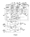
- FIG. 9 shows a schematic of the analog portions of the circuitry illustrated in FIG. 7, including the current mirror 416, the current driver 414, the voltage/pacing driver 412, the pacing return amp 422 and the red and IR sample and hold circuitry 418 and 420, respectively.
- the current and voltage regulator circuits used in the current driver 414 and voltage pacing driver 412 are based upon a common design often found in audio power amplifier output stages.
- the operation of the circuitry in FIG. 9 is best understood in conjunction with the timing diagram of FIG. 10. In the following description, all reference numbers of 600 or higher refer to FIG. 10. Starting with a pace signal 600 indicating time out of the escape interval of the pacemaker, on line 448, the pacing return amp 422 is activated.
- the pace signal 600 applies a current across LED 542 via resistor 544, which activates phototransistors 552 which turns on transistor 548 driving PACE RETURN line 548 high at 604 and simultaneously driving PACE DRIVE line 402 low via transistor 540, allowing discharge of output capacitor 554 through transistor 548, PACE RETURN line 458, electrode 424 (FIG. 7), electrode 410 (FIG. 7), PACE DRIVE line 402 and transistor 540.
- the pace signal 600 also takes the reset off decade counter 462 which begins the timing of the sensing cycle. After the pace signal 600, the Q output of flip-flop 466 (FIG.
- the IR SAMPLE line 444 goes high at 618, allowing the output of current mirror 416 on line 456 to be sampled by the IR sample and hold circuitry 418.
- the IR sample and hold circuitry consists of an analog switch 558 which, when activated by a signal on IR SAMPLE line 444 passes the voltage on line 456 to op amp 568 and capacitor 562.
- the sample and hold system does not operate in the classical sense of sampling until the hold capacitor 562 reaches the exact input voltage. Instead, the sample time is only a small fraction of the time constant of the source resistance and the holding capacitor 562.
- the line 452 goes low at 620 and the IR line 454 goes low at 622.
- This change turns off transistors 540 and 536 in the voltage/pacing driver 412 and turns on transistors 532 and 534, sending the PACE/DRIVE line 402 high at 624.
- transistors 508 and 512 are turned off while transistors 518 and 522 are turned on applying LED current of the opposite polarity of approximately 20 milliamps at 628 across red LED 236.
- COMMON line 404 goes to one LED drop below battery voltage at 626.
- red LED 236 Light reflected from red LED 236 allows current to flow through phototransistor 234 at 630, which, via RETURN line 406 and current mirror 416 provides a proportional voltage on line 456.
- the RED SAMPLE line 446 goes high at 632, enabling the red sample and hold circuitry 420, which includes an analog switch 556, capacitor 560 and an op amp 566, which function in a fashion identical to that of the circuitry discussed in conjunction with the IR sample and hold circuitry 418.
- the voltage on PACE RETURN line 458 follows the voltage on PACE/DRIVE line 402, preventing current flow between electrode 410 (FIG. 7) and electrode 424 (FIG. 7).
- the voltage on COMMON line 404 changes at the point LED 238 is turned on. Because phototransistor 234 has a large collector-base capacitance, if the voltage across collector and emitter decreases, transistor 234 will temporarily shut off for a period long enough to discharge this capacitance. Therefore, the circuitry herein has been arranged to provide an increase in voltage, rather than a decrease, at the point the voltage on COMMON line 404 changes. Transients due to the COMMON line 404 voltage change do not appear to be significant at light levels generated by high efficiency LED's as described herein.
- the voltages on RED OUT line 432 and IR OUT line 430 are fed to the IR/R division network 428 to produce an analog DC voltage signal on line 434 (FIG. 7) indicative of oxygen saturation.
- This signal on line 434 is provided to sensor processing circuitry 30 (FIG. 1) and used to regulate the escape interval of the pacemaker as described above.
- IR line 454 goes high at 658 causing PACE/DRIVE line 402 to go low at 650 providing a current of approximately 20 milliamps at 656 across IR diode 538.
- COMMON line 402 goes to an LED drop above ground at 654. This allows a current to flow through photo transistor 534 and 658 which is samples while the IR SAMPLE line 444 is high at 660. Halfway through the sampling cycle at the count of 5 on the decade counter 462 (FIG.
- RED line 452 goes low at 662, along with IR line 454, driving PACE/DRIVE line 402 high at 664 and allowing a current of approximately 20 milliamps at 670 to flow across the red diode 238 (FIG. 7).
- COMMON line 404 goes to one LED drop below battery voltage at 666. Light received from red diode 238 (FIG. 7) allows current to flow through phototransistor 234 (FIG. 7) at 672, which is samples while RED SAMPLE line 446 is high, at 674. Again, the voltage on PACE RETURN line 458 follows the voltage on PACE/DRIVE line 402, avoiding current flow between tip electrode 410 (FIG. 7) and electrode 424 (FIG. 7).
- FIGs. 8 and 9 The particular circuitry disclosed in FIGs. 8 and 9 is optimized for use with a lithium thionylchloride battery providing a supply voltage of 3.6 volts. However, functionally similar circuitry adapted for use with batteries of other voltages is believed to be within the scope of the present invention. In addition, in those embodiments in which lower voltage batteries are used, it may be desirable to incorporate a voltage doubler in the pacing return amplifier, in order to provide adequate voltage to capture the heart. The present invention is also believed broad enough to encompass such embodiments. It is also acknowledged that there are numerous alternative ways of providing the time periods provided by the circuitry of FIG. 8, and the other analog and/or digital equivalents of this circuitry are believed to also be within the scope of the present invention.
Abstract
Description
- The present invention relates generally to medical devices and more specifically relates to implantable electronic devices for muscle stimulation.
- The earliest implantable pacing systems operated asynchronously to normal physiologic functions. U.S. Patent No. 3,057,356, issued to Greatbatch, teaches such a pacemaker which includes a fixed rate oscillator which determines an escape interval. At the expiration of each escape interval, a pacing pulse is generated. Subsequent designs, such as in U.S. Patent No. 3,478,746 issued to Greatbatch, incorporated a sense amplifier coupled to the pacing electrode, which sensed the electrical activity indicative of a contraction of the heart and reset the oscillator to restart timing the escape interval. These pacemakers, called demand pacemakers, only paced if no natural contractions were sensed within the escape interval.
- As an alternative to regulating pacing rate by sensing the contractions of the heart, some pacemakers have regulated rate in response to measurement of some other, physiological parameter. There have been pacemakers proposed which vary rate in response to instantaneous blood pressure within the right atrium, as in U.S. Patent No. 3,358,690, in response to respiration as in U.S. Patent No. 3,593,718, in response to physical activity as in U.S. Patent No. 4,140,132 or in response to neurological activity as in U.S. Patent No. 4,210,219. The most promising techniques appear to involve varying of pacing rate in response to sensing of chemical parameters of the blood. For example, U.S. Patent No. 4,009,721 and U.S. Patent No. 4,252,124 teach pacemakers in which an implantable pH sensor determines the rate of the pacing oscillator. U.S. Patent No. 4,202,339 issued to Wirzfeld and U.S. Patent No. 4,339,820 issued to Wirtzfeld et al, both teach a pacing system in which the rate of an asynchronous pacing oscillator is controlled by the oxygen level of the intracardiac venous blood. U.S. Patent No. 4,467,807 issued to Bornzin combines the techniques of varying the rate of the pacemaker in response to sensed oxygen with the demand function, so that an interaction of both of these factors determines the delivery of pacing impulses by the pacemaker.
- The present invention comprises an improved oxygen sensor and associated circuitry for use within a cardiac pacemaker of the type in which pacing rate is dependent upon the percentage of oxygen saturation of the intracardiac venous blood.
- The preferred embodiment includes a hermetically sealed sensor capsule containing a two wavelength reflectance oximeter. The method of construction of this capsule assures its suitability for long term human implant. In addition, the invention includes timing, processing and output circuitry for operating the sensor in a predetermined time relationship with pacing output pulses and which allows the construction of a long term implantable lead which performs EKG sensing, cardiac pacing and two wave length reflectance oximetry using only three conductors. Minimizing the number of conductors is believed particularly valuable in long term implantable devices, where experience has shown that electronic complexity is preferable to mechanical complexity.
- An example of the invention will now be described with reference to the accompanying drawings.
- FIG. 1 is an illustration of a prior art rate adaptive demand pacemaker in which sensed oxygen saturation is used to regulate the pacing rate.
- FIG. 2 is a plan view of a pacing and oxygen sensing lead according to the present invention.
- FIG. 3 is a side sectional view of the sensor body, a subassembly of the sensor capsule.
- FIG. 4 is a side sectional view of the window assembly, a subassembly of the sensor capsule.
- FIG. 5 is a side sectional view through the completed sensor capsule.
- FIG. 6 is a top sectional view through the completed sensor capsule.
- FIG. 7 is a functional diagram of the sensor and associated circuitry.
- FIG. 8 is a schematic of the digital timing circuitry associated with the sensor capsule.
- FIG. 9 is a circuit diagram of the analog circuitry associated with the sensor.
- FIG. 10 is a timing diagram illustrating the operation of the sensor capsule, and its relation to the operation of the cardiac pacemaker with which it is intended to be employed.
- FIG. 1 illustrates a rate adaptive demand pacemaker in which sensed oxygen level is used to vary the escape interval of a demand pacemaker, as disclosed in U.S. Patent No. 4,467,807 issued to Bornzin. This figure is intended both to illustrate pertinent prior art in this area and to provide a general illustration of how the circuitry and sensor of the present invention may be functionally related to the circuitry of an implantable pacemaker.
- FIG. 1 shows a single chamber pacing system including a
sensor 12 within theright ventricle 20 ofheart 10, which generates a voltage online 14 proportional to percentage of oxygen saturation in the right ventrical of the heart. The voltage online 14 is processed bysensor processing circuitry 30 which includes an analog to digital converter which converts the voltage online 14 to a binary number which is used to control the pacing rate set bydemand logic 106 andfixed rate oscillator 112.Line 104 is coupled to an electrode inright ventricle 20 of theheart 10 and delivers electrical signals to thesense amplifier 102 which generates an output online 108 indicative of the sensing of a natural contraction of the human heart. On sensing such a contraction, the timing period of the demand logic is reset. On expiration of the escape interval determined bydemand logic 106 andfixed rate oscillator 112 under the control ofsensor processing 30, a signal is generated online 34 which triggersdriver 26 to produce a stimulating pulse vialine 16, to be applied to anelectrode 18 within the right ventricle of theheart 10. A detailed description of the circuitry employed insensor processing block 30 anddemand logic 106 can be found in U.S. Patent No. 4,467,807 at column 3, lines 59-68,column 4, lines 1-68 andcolumn 5, lines 1-30. - Although the incorporation of the present invention in an implantable pacemaker is discussed specifically with reference to the pacemaker disclosed in FIG. 1, the invention is believed equally applicable to other pacemakers employing alternate circuitry configurations for determining rate in response to an analog signal indicative of oxygen saturation. For example, it is believed the invention would also be useful in conjunction with a pacemaker as disclosed in U.S. Patent No. 4,202,339 issued to Wirtzfeld, cited above. Specifically, the invention may be used in asynchronous pacemakers, i.e. those without a demand function.
- FIG. 2 is a plan view of a permanently implantable lead according to the present invention.
Lead 200 is provided with apacing electrode 210 at its extreme distal tip, which is held in place within the heart bytines 212, which may be of the type described in U.S. Patent No. 3,902,501 issued to Citron et al or U.S. Patent No. 4,269,198 issued to Stokes. Located proximal toelectrode 210 is asensor capsule 214, which contains a two wavelength reflectance oximeter. Capsule 214 is spaced fromelectrode 210 by aninsulative lead body 216 which encloses a conductor which coupleselectrode 210 tosensor capsule 214. Proximal tosensor 214 is anelongated lead body 218 which is preferably sheathed in a pliant, insulative material such as polyurethane or silicone rubber.Lead body 218 contains three coaxially mounted coiled conductors coupled tosensor capsule 214 and extended toconnector assembly 220.Connector assembly 220 includes threeconnector surfaces lead body 218. Ananchoring sleeve 228 is optionally included to stabilizelead 200 at the point of venous insertion. Anchoringsleeve 228 may be of the type described in U.S. Patent No. 4,437,475 issued to White. - FIG. 3 is a side sectional view of the sensor body assembly, a subassembly of the
sensor capsule 214 of the present invention. The sensor body assembly includes a machinedtitanium sensor body 230, havinglongitudinal surface 231 which serves to mount theceramic substrate 232 upon which the various electronic elements of the two frequency reflectance oximeter are located. These elements include aphototransistor 234, an infraredlight emitting diode 236 and a redlight emitting diode 238.Diodes phototransistor 234 by asemicircular wall 240. At the proximal end ofsensor body 230 is anaperture 242 in which a sapphire orglass feedthrough 246 is located. Feedthrough 246 has been brazed tosensor body 230 around its entire circumference, using a braze such as gold. Extending through and also brazedfreedthrough 246 are two wires, of which only one, labeled 248, is visible in this view.Wire 248 is soldered to a conductive pad located on ceramic 232. At the distal end ofsensor body 230 is abore 250 which serves as a mounting point for a coiled conductor. - FIG. 4 is a side sectional view of the window assembly of the sensor capsule. The window assembly includes an optically pure sapphire or
glass tube 252 and twowelding collars tube 252.Welding collars sapphire tube 252.Welding collars sapphire tube 252 around their entire circumference, using a braze which is preferably gold. Prior to brazing, the proximal and distal ends oftube 252 are coated with a thin film of niobium or similar metalization to facilitate brazing. Vapor deposition or sputtering techniques may be used to provide this thin film. - The capsule itself is assembled by sliding the window assembly of FIG. 4 proximally over the body assembly of FIG. 3, until the
proximal end 258 ofweld collar 254 is adjacent theshoulder 243 of sensor body 230 (FIG. 3) The inner diameter of thedistal portion 260 ofweld collar 256 is the same as the outer diameter of thedistal portion 310 ofsensor body 230. After assembly,weld collar 254 andweld collar 256 may conveniently be laser welded tosensor body 230, around the circumference ofproximal end 258 ofweld collar 254 and ofdistal end 260 ofweld collar 256. The circular cross sections ofweld collars sensor body 230 at the weld points simplifies the weld process by allowing the assembly to simply be rotated under the welding beam. Laser welding is the preferred method, but other methods such as electron beam welding may also be appropriate. This procedure produces a hermetically sealed sensor capsule appropriate for a long term implant within the human body. The use of titanium for both thesensor body 230 and for theweld collars - FIG. 5 is a side sectional view of the sensor capsule, mounted in the lead of FIG. 2. Within
bore 250 at the distal end ofsensor body 230 is located acoiled conductor 262 which is held in place bycrimps 264 which mechanically and electrically couple it tosensor body 230.Conductor 262 extends to and is electrically coupled with tip electrode 210 (FIG. 2). - At the proximal end of the sensor body is a
capsule adapter 268, which is laser welded at its distal end tosensor body 230 andwelding collar 254.Capsule adapter 268 is generally cylindrical and hollow in its construction, and includes across bore 270 for addition ofbackfill material 271. Welded to acapsule adapter 268 is acoiled conductor 272, which is coupled to connector pin 226 (FIG. 2). Located within theinternal cavity 269 ofadapter 268 are two, mutually insulated coaxially coiled conductors includingcoiled conductor 274 and coiledconductor 276, which are insulated by insulatingsheaths Conductor 276 is attached to wire 248, within a welding sleeve, not visible in this illustration.Conductor 274 is coupled to asecond wire 247, passing throughfeedthrough 246. The entire lead is sheathed in anouter insulative sheath 282, which is preferably fabricated of polyurethane or other transparent, non-thrombogenic material.Cavity 269 is backfilled withepoxy 271. All other labeled elements correspond to identically numbered elements in FIGs. 3 and 4, above. - FIG. 6 is a top cut away view of the sensor capsule mounted in the lead of FIG. 2. In this view, the connection of
conductors wires Conductors wires welding sleeves wires metallic pads substrate 232.Phototransistor 234 is seen to be mounted on aconductive pad 292, coupled tometallic pad 290.Phototransistor 234 is coupled by means of a fine wire 294 to a second conductive pad 296, coupled tometallic pad 288.Conductive pad 292 extends underwall 240, and serves as the mounting point forinfrared LED 236. A thirdconductive pad 298 serves as a mounting point forred LED 238. LED's 236 and 238 are connected topads fine wires 300 and 302.Conductive pad 298 is coupled to a fourthconductive pad 304 by means of afine wire 306 andpad 304 is coupled tosensor body 230 bymetallic strap 239. All other elements correspond to identically numbered elements in FIG. 3, 4 and 5. - FIG. 7 is a functional diagram of the sensor and its associated circuitry. In this view, the sensor hybrid 400 is illustrated schematically, showing the interconnection of
infrared LED 236,red LED 238 andphototransistor 234. The threelines coiled conductors Line 408 corresponds toconductor 262, shown in FIG. 5 and electrode 410 corresponds to tipelectrode 210, shown in FIG. 2. - The
diode pair amplifiers Amplifier 412 operates in a voltage output mode, andamplifier 414 operates in a current output mode. The returning current fromphototransistor 234 is converted to a proportional DC voltage by thecurrent mirror 416 and is delivered to the sample and holdswitches 418 and 420 which recover the peak signal for each color. Pacing is accomplished by placingline 402 fromvoltage driver 412 at alogic 0 and placingline 458 to return amplifier 422 at alogic 1. For example, if the system employs a 3.6 volt lithium thionylchloride cell, this produces a pacing voltage of approximately 3.1 volts across the heart. Pacingreturn amplifier 422 is coupled toelectrode 424, which may conveniently be the metal enclosure of the implanted pacemaker. Timing for the entire system is provided by integrated circuitry included in thetiming block 246, which controls the timing and function of thepacing voltage driver 412 and thecurrent driver 414 as well as determining times for operation of the sample and holdcircuits 418 and 420. The outputs of sample and holdcircuits 418 and 420 are coupled to a division network 428 which divides the output of IR sample and hold 420 online 430 by the output of red sample and hold 418 online 432 to produce a D.C. voltage signal online 434 indicative of the percentage of oxygen saturation. IR/R division network 428 may be of the type illustrated in FIG. 1 of U.S. Patent No. 4,202,339 issued to Wirtzfeld et al. In particular, it may correspond to the division network labeled 16, and described in column 3, lines 30-36.Line 434, carrying an analog signal indicative of oxygen saturation may be coupled to the sensor processing circuitry of a pacemaker such as illustrated in FIG. 1. The sensor and associated circuitry may replace thesensor 12 andline 14 of FIG. 1, with the output of IR/R division network 428 functionally coupled tosensor processing circuitry 30. - The functional interconnection of the circuitry of FIG. 7 with the remainder of the circuitry of an implantable cardiac pacemaker is also described in conjunction with the prior art pacemaker illustrated in FIG. 1. Sensor operation under control of
timing circuit 426 may conveniently be initiated in response to a signal online 448 indicative of the occurrence of a cardiac pacing pulse of a signal online 438 indicative of a sensed spontaneous contraction of the heart. The input to timing 426 online 448 therefore might be functionally coupled to the output ofdemand logic 106 online 34 and the input to timing 426 online 438 might be functionally coupled to the output ofsense amplifier 102 online 108.Return pacing amp 422 may be functionally coupled to demandlogic 106 so as to be activated by a signal online 448 indicative of time out of the escape interval. Finally, electrode 410 may be coupled vialine 442 to theinput sense amp 102 online 104 so that electrode 410 also acts as an EKG sensing electrode. - FIG. 8 is a schematic of a timing circuit for use with the sensor lead of FIGs. 2-6.
Decade counter 462 serves to time the application of the current to the infrared and red LEDs in the sensor capsule as well as defining sampling periods during the operation of the red and infrared LEDs. The basic operation is as follows: Following a signal online flop 466 is set via ORgate 468, which removes the reset fromcounter 462, allowing it to be clocked by10KHz clock 460, and driving the signal onIR line 454 to alogic 1 via ANDgate 472. - When the signal on
line 454 is high, current is applied to activate theinfrared LED 236. During counts 1, 2 and 3 ofdecade counter 426, theIR SAMPLE line 444 is driven to alogic 1 via ORgate 476. During counts 1, 2 and 3, the IR sample and hold circuitry is activated. At a count of 5, the CARRY output ofdecade counter 462 goes to alogic 0, driving the signal on the
line 542 tologic 0, and also driving the signal onIR line 454 to alogic 0 via ANDgate 472. While the signal on
line 452 is at alogic 0, current is applied to drive the red LED. During counts 6, 7 and 8 ofdecade counter 462, theRED SAMPLE line 446 goes to alogic 1, via ORgate 482. During counts 6, 7 and 8, the red sample and hold circuitry is activated. On a count of 9, the set reset flip-flop 466 is reset, lockingdecade counter 462 on reset and driving
line 452 high, ending delivery of current to the red LED. Thus, this circuitry provides timing for driving the infrared and red LEDs in sequence, and sampling each diode during the center portion of the period during which they are driven. This sequence of events occurs a fixed time after either a pulse signal online 448 or a sense signal online 438, which assures that the oxygen level is sampled once per each heartbeat, without running the risk of attempting to sense the oxygen level during a pacing pulse or resetting the pulse generator timing in response to electrical currents driven through the sensor. - FIG. 9 shows a schematic of the analog portions of the circuitry illustrated in FIG. 7, including the
current mirror 416, thecurrent driver 414, the voltage/pacing driver 412, thepacing return amp 422 and the red and IR sample and holdcircuitry 418 and 420, respectively. The current and voltage regulator circuits used in thecurrent driver 414 andvoltage pacing driver 412 are based upon a common design often found in audio power amplifier output stages. The operation of the circuitry in FIG. 9 is best understood in conjunction with the timing diagram of FIG. 10. In the following description, all reference numbers of 600 or higher refer to FIG. 10. Starting with apace signal 600 indicating time out of the escape interval of the pacemaker, online 448, thepacing return amp 422 is activated. Thepace signal 600 applies a current acrossLED 542 viaresistor 544, which activatesphototransistors 552 which turns ontransistor 548 drivingPACE RETURN line 548 high at 604 and simultaneously drivingPACE DRIVE line 402 low viatransistor 540, allowing discharge ofoutput capacitor 554 throughtransistor 548,PACE RETURN line 458, electrode 424 (FIG. 7), electrode 410 (FIG. 7),PACE DRIVE line 402 andtransistor 540. In addition, as discussed in conjunction with FIG. 8, above, thepace signal 600 also takes the reset offdecade counter 462 which begins the timing of the sensing cycle. After thepace signal 600, the Q output of flip-flop 466 (FIG. 8) goes high, drivingIR line 454 high at 608, turning ontransistors DRIVE line 402 low at 610 and turning ontransistors COMMON line 404 goes to one LED drop above ground at 612. This in turn triggerscurrent flow 616 through phototransistor 234 (FIG. 7) and which, viaRETURN line 406 is applied tocurrent mirror 416. The currentmirror comprising transistors resistor 504 generates an output signal on line 456. During counts 2-4 of decade counter 462 (FIG. 8), theIR SAMPLE line 444 goes high at 618, allowing the output ofcurrent mirror 416 on line 456 to be sampled by the IR sample and hold circuitry 418. The IR sample and hold circuitry consists of ananalog switch 558 which, when activated by a signal onIR SAMPLE line 444 passes the voltage on line 456 toop amp 568 andcapacitor 562. The sample and hold system does not operate in the classical sense of sampling until thehold capacitor 562 reaches the exact input voltage. Instead, the sample time is only a small fraction of the time constant of the source resistance and the holdingcapacitor 562. In this way, in response to any abrupt voltage swings on line 456, thecapacitor 562 swings only part way to the final value during each sample, but after a series of samples will converge on the actual source voltage value. This mode of operation is believed appropriate in that the oxygen saturation level changes between successive samples is small compared to the overall capacity ofcapacitor 562. This approach has the advantage that it minimizes power consumption and circuit complexity. - On the fifth clock cycle counted by decade counter 462 (FIG. 8), the

line 452 goes low at 620 and theIR line 454 goes low at 622. This change turns offtransistors pacing driver 412 and turns ontransistors DRIVE line 402 high at 624. In addition,transistors transistors 518 and 522 are turned on applying LED current of the opposite polarity of approximately 20 milliamps at 628 acrossred LED 236.COMMON line 404 goes to one LED drop below battery voltage at 626. Light reflected fromred LED 236 allows current to flow throughphototransistor 234 at 630, which, viaRETURN line 406 andcurrent mirror 416 provides a proportional voltage on line 456. During count 6, 7 and 8 ofdecade counter 462, theRED SAMPLE line 446 goes high at 632, enabling the red sample and holdcircuitry 420, which includes ananalog switch 556,capacitor 560 and anop amp 566, which function in a fashion identical to that of the circuitry discussed in conjunction with the IR sample and hold circuitry 418. Due to the high impedance of thepacing return amp 422 when inactive, the voltage onPACE RETURN line 458 follows the voltage on PACE/DRIVE line 402, preventing current flow between electrode 410 (FIG. 7) and electrode 424 (FIG. 7). - In order for the specific embodiment of circuitry illustrated to function properly, it is necessary that high efficiency LED's be used which preferably limit voltage across the LED's to approximately 1.6 volts. This places
COMMON line 404 at approximately 1.6 volts during operation ofLED 236 and at approximately 2.0 volts during operation ofLED 238. This assures adequate bias forphototransistor 234. - As noted above, the voltage on
COMMON line 404 changes at thepoint LED 238 is turned on. Becausephototransistor 234 has a large collector-base capacitance, if the voltage across collector and emitter decreases,transistor 234 will temporarily shut off for a period long enough to discharge this capacitance. Therefore, the circuitry herein has been arranged to provide an increase in voltage, rather than a decrease, at the point the voltage onCOMMON line 404 changes. Transients due to theCOMMON line 404 voltage change do not appear to be significant at light levels generated by high efficiency LED's as described herein. - The voltages on
RED OUT line 432 andIR OUT line 430 are fed to the IR/R division network 428 to produce an analog DC voltage signal on line 434 (FIG. 7) indicative of oxygen saturation. This signal online 434 is provided to sensor processing circuitry 30 (FIG. 1) and used to regulate the escape interval of the pacemaker as described above. - Similarly, after the
signal 646 onSENSE line 438,IR line 454 goes high at 658 causing PACE/DRIVE line 402 to go low at 650 providing a current of approximately 20 milliamps at 656 acrossIR diode 538.COMMON line 402 goes to an LED drop above ground at 654. This allows a current to flow throughphoto transistor IR SAMPLE line 444 is high at 660. Halfway through the sampling cycle at the count of 5 on the decade counter 462 (FIG. 8),RED line 452 goes low at 662, along withIR line 454, driving PACE/DRIVE line 402 high at 664 and allowing a current of approximately 20 milliamps at 670 to flow across the red diode 238 (FIG. 7).COMMON line 404 goes to one LED drop below battery voltage at 666. Light received from red diode 238 (FIG. 7) allows current to flow through phototransistor 234 (FIG. 7) at 672, which is samples whileRED SAMPLE line 446 is high, at 674. Again, the voltage onPACE RETURN line 458 follows the voltage on PACE/DRIVE line 402, avoiding current flow between tip electrode 410 (FIG. 7) and electrode 424 (FIG. 7). - The following components were used to construct the circuitry illustrated in FIGS. 7, 8 and 9:

- The particular circuitry disclosed in FIGs. 8 and 9 is optimized for use with a lithium thionylchloride battery providing a supply voltage of 3.6 volts. However, functionally similar circuitry adapted for use with batteries of other voltages is believed to be within the scope of the present invention. In addition, in those embodiments in which lower voltage batteries are used, it may be desirable to incorporate a voltage doubler in the pacing return amplifier, in order to provide adequate voltage to capture the heart. The present invention is also believed broad enough to encompass such embodiments. It is also acknowledged that there are numerous alternative ways of providing the time periods provided by the circuitry of FIG. 8, and the other analog and/or digital equivalents of this circuitry are believed to also be within the scope of the present invention.
Claims (29)
sensing means for sensing naturally occurring heart signals and generating a reset signal;
pulse generator means for generating stimulating pulses at a minimum pacing rate, including first timing means for providing each stimulating pulse separated by an escape interval corresponding to the pacing rate and reset means responsive to a reset signal for resetting said timing means and restarting the escape interval;
means for measuring blood oxygen level and for providing an escape interval modifying signal;
means responsive to the escape interval modifying signal for adjusting the escape interval to provide pacing pulses on demand at a minimum rate correlating to the cardiac output requirements of the patient;
characterised in that said blood oxygen level measuring means comprises:
a sensor capsule means for location in the bloodstream, including a first light source generating light at a first wavelength, a second light source generating light at a second wavelength and a light responsive means for generating a light level signal indicative of the intensity of the light impinging upon said light responsive means, said first and second light sources and said light responsive means being mounted within said sensor capsule means, said sensor capsule means being at least partially transparent such that light generated by said first and second light sources may pass through said capsule body into said bloodstream and such that light reflected by said bloodstream may pass through said sensor capsule means to impinge upon said light responsive means;
second timing means coupled to said sensing means and to said pulse generator means for determining a first time interval following said reset signals and following said stimulating pulses, for determining a second time interval following said first time interval, for generating a first sampling signal during said first time interval and for generating a second sampling signal during said second time interval;
light source driving means coupled to said second timing means and to said first and second light sources for activating said first light source during said first time interval and for activating said second light source during said second time interval;
first sample and hold means coupled to said second timing means and to said light responsive means, responsive to said first sampling signal for sampling said light level signal and for holding a first value derived from said sampled light level signal; and
second sample and hold means coupled to said second timing means and to said light responsive means, responsive to said second sampling signal for sampling said light level signal and for holding a second value derived from said sampled light level signal; and
wherein said adjusting means is coupled to said first and second sample and hold means and wherein said adjusting means adjusts said escape interval in response to said first and second values stored in said first and second sample and hold means.
pulse generator means for generating stimulating pulses at a minimum pacing rate including first timing means for providing each stimulating pulse separated by an escape interval corresponding to the pacing rate;
means for measuring blood oxygen level and for providing an escape interval modifying signal for adjusting the escape interval to provide pacing pulses at a minimum rate correlated to the cardiac output requirements of the patient;
characterised in that said blood oxygen level measuring means comprises:
a sensor capsule means for location in the bloodstream, including a first light source generating light at a first wavelength, a second light source generating light at a second wavelength and a light responsive means for generating a light level signal indicative of the intensity of the light impinging upon said light responsive means, said first and second light sources and said light responsive means being mounted within said sensor capsule means, said sensor capsule means being at least partially transparent such that light generated by said first and second light sources may pass through said capsule body into said bloodstream and such that the light reflected by said bloodstream may pass through said sensor capsule means to impinge said light responsive means;
second timing means coupled to said pulse generator means for determing a first time interval following said stimulating pulses, for determining a second time interval following said first time interval, for generating a first sampling signal during said first time interval and for generating a second sampling signal during said second time interval;
light source driving means coupled to said second timing means and to said first and second light sources for activating said first light source during said first time interval and for activating said second light source during said second time interval;
first sample and hold means coupled to said second timing means and to said light responsive means and responsive to said first sampling signal for sampling said light level signal and for holding a first value derived from said sample light level signal;
second sample and hold means coupled to said second timing means and to said light responsive means and responsive to said second sampling signal for sampling said light level signal and for holding a second value derived from said sample light level signal, wherein said adjusting means is coupled to said first and second sample and hold means and wherein said adjusting means adjusts said escape interval in response to said first and second values stored in said first and second sample and hold means; and
wherein said pulse generator means includes an electrode electrically coupled to said first and second light sources.
a sensor capsule having an interior,
a proximal end and a distal end, said sensor capsule comprising a conductive sensor body extending the length of said sensor capsule and exposed to the exterior of said sensor capsule at the proximal and distal ends of said sensor capsule;
electronic circuitry means for sensing a physiological parameter of the bloodstream, mounted within said sensor capsule and electrically coupled to said sensor body;
a first elongate electrical conductor extending proximally from said sensor capsule and electrically coupled to said sensor body at the proximal end of said sensor capsule;
a second elongate conductor, insulated from said first conductor and extending proximally from the proximal end of said sensor capsule, said second conductor extending into the interior of said sensor capsule and being electrically coupled to said circuitry means;
a third conductor electrically coupled to said sensor body at the distal end of said sensor capsule and extending distally from said sensor capsule;
an electrode coupled to said third conductor; and
an elongate insulative lead body enclosing said first and second conductors, said sensor capsule and said third conductor, said electrode being exposed to the exterior of said insulative lead body.
a first light emitting diode electrically coupled between said sensor body and said second conductor;
a second light emitting diode electrically coupled between said sensor body and said second conductor parallel to but with an opposite polarity to said first light emitting diode; and
a phototransistor coupled between said second and fourth conductors and insulated from said sensor body.
a sensor capsule comprising a first light emitting diode emitting light of a first wavelength, a second light emitting diode emitting light of a second wavelength and a semiconductor means for regulating flow of current dependent upon the amount of light impinging on said semiconductor means;
first and second conductors electrically coupled to said first and second light emitting diodes such that said first and second light emitting diodes are electrically coupled between said first and second conductors but with opposite polarities, and second conductor being electrically coupled to said semiconductor means;
a third conductor electrically coupled to said semiconductor means such that said semiconductor means is electrically coupled between said second and third conductors;
first voltage generating means for generating a voltage differential between said first and second conductors of a first polarity and for simultaneously generating a voltage differential between said second and third conductors of said first polarity;
second voltage generating means for generating a voltage differential between said first and second conductors of a second polarity and for simultaneously generating a voltage differential between said second and third conductors of said first polarity; and
current measuring means coupled to said second and third conductors for measuring current flow through said semiconductors means.
means for enabling said sequential activating means following generation of said stimulating pulse.
a first electrode coupled to said first conductor;
a second electrode, insulated from said first conductor;
pulse generator means coupled to said first conductor and to said second electrode for generating a stimulating pulse across said first and second electrodes.
selecting a circular cylindrical tube of transparent material having a proximal end, a distal end, and a circular lumen from said proximal end to said distal end, and having a melting point sufficiently high to permit brazing thereto;
selecting a metal proximal weld collar having a proximal end, a distal end, and a circular lumen extending from said proximal end to said distal end, the proximal end of the lumen of said weld collar having a first diameter at the proximal end of said weld collar and having a circumferential indentation in the distal end surface of said weld collar, said circumferential indentation corresponding to the proximal end of said tube;
selecting a metal distal weld collar having a proximal end, a distal end and a circular lumen extending from said proximal end to said distal end, the lumen of said weld collar having a second diameter at the distal end of said weld collar and a circumferential indentation in the proximal end surface of said weld collar, said circumferential indentation corresponding to the distal end of the tube;
selecting a metal body having a proximal end and a distal end and having electronic circuitry attached thereto intermediate said proximal and distal ends of said body, said proximal end of said body having a circular cross section of said first diameter and said distal end of said body having a circular cross section of said second diameter, the length of said body exceeding the length of said tube;
inserting the proximal end of said tube into the circular indentation in the distal end of said proximal weld collar and inserting the distal end of said tube into the indentation at the proximal end of said distal weld collar;
brazing said proximal and distal weld collars to said tube;
after said brazing step, sliding said tube and said weld collars over said body such that the proximal end of said body extends proximally to the proximal end of said proximal weld collar and such that the distal end of said body extends distally to the distal end of said distal weld collar; and
after said sliding step, welding the distal end of said distal weld collar to the distal end of said body and said proximal end of said proximal weld collar to the proximal end of said body.
Applications Claiming Priority (4)
| Application Number | Priority Date | Filing Date | Title |
|---|---|---|---|
| US06/896,695 US4791935A (en) | 1986-08-15 | 1986-08-15 | Oxygen sensing pacemaker |
| US06/896,693 US4730389A (en) | 1986-08-15 | 1986-08-15 | Method for fabrication of an implantable hermetic transparent container |
| US896693 | 1986-08-15 | ||
| US896695 | 2001-06-28 |
Publications (3)
| Publication Number | Publication Date |
|---|---|
| EP0257954A2 true EP0257954A2 (en) | 1988-03-02 |
| EP0257954A3 EP0257954A3 (en) | 1988-08-10 |
| EP0257954B1 EP0257954B1 (en) | 1993-06-16 |
Family
ID=27129150
Family Applications (1)
| Application Number | Title | Priority Date | Filing Date |
|---|---|---|---|
| EP19870307263 Expired - Lifetime EP0257954B1 (en) | 1986-08-15 | 1987-08-17 | Oxygen sensing pacemaker |
Country Status (2)
| Country | Link |
|---|---|
| EP (1) | EP0257954B1 (en) |
| DE (1) | DE3786210T2 (en) |
Cited By (7)
| Publication number | Priority date | Publication date | Assignee | Title |
|---|---|---|---|---|
| EP0314937A2 (en) * | 1987-10-08 | 1989-05-10 | Pacesetter AB | Implantable blood oxygen sensor and method of use |
| EP0413588A2 (en) * | 1989-08-17 | 1991-02-20 | Critikon, Inc. | Epidural oxygen sensor |
| EP0416469A2 (en) * | 1989-09-05 | 1991-03-13 | Pacesetter, Inc. | Oxygen content pacemaker sensor and method |
| EP0518364A2 (en) | 1991-06-14 | 1992-12-16 | Pacesetter, Inc. | Pacemaker lead for sensing a physiologic parameter of the body |
| US8388670B1 (en) | 2007-01-16 | 2013-03-05 | Pacesetter, Inc. | Sensor/lead systems for use with implantable medical devices |
| US8709631B1 (en) | 2006-12-22 | 2014-04-29 | Pacesetter, Inc. | Bioelectric battery for implantable device applications |
| CN107380347A (en) * | 2017-07-28 | 2017-11-24 | 吴昊 | A kind of warship, ship, ship intelligent escape window system |
Citations (6)
| Publication number | Priority date | Publication date | Assignee | Title |
|---|---|---|---|---|
| EP0005312A2 (en) * | 1978-03-13 | 1979-11-14 | Medtronic, Inc. | Gold alloys, a method of brazing and articles formed thereby |
| US4202339A (en) * | 1977-04-21 | 1980-05-13 | Alexander Wirtzfeld | Cardiac pacemaker |
| WO1980001620A1 (en) * | 1979-01-29 | 1980-08-07 | Medtronic Inc | Hermetic electrical feedthrough assembly |
| US4399820A (en) * | 1981-02-26 | 1983-08-23 | Alexander Wirtzfeld | Process and device for regulating the stimulation frequency of heart pacemakers |
| US4467807A (en) * | 1981-11-23 | 1984-08-28 | Medtronic, Inc. | Rate adaptive demand pacemaker |
| EP0247296A1 (en) * | 1986-05-22 | 1987-12-02 | Siemens Aktiengesellschaft | Cardiac measuring device for determining the oxygen saturation in blood |
-
1987
- 1987-08-17 EP EP19870307263 patent/EP0257954B1/en not_active Expired - Lifetime
- 1987-08-17 DE DE19873786210 patent/DE3786210T2/en not_active Expired - Fee Related
Patent Citations (7)
| Publication number | Priority date | Publication date | Assignee | Title |
|---|---|---|---|---|
| US4202339A (en) * | 1977-04-21 | 1980-05-13 | Alexander Wirtzfeld | Cardiac pacemaker |
| EP0005312A2 (en) * | 1978-03-13 | 1979-11-14 | Medtronic, Inc. | Gold alloys, a method of brazing and articles formed thereby |
| WO1980001620A1 (en) * | 1979-01-29 | 1980-08-07 | Medtronic Inc | Hermetic electrical feedthrough assembly |
| US4399820A (en) * | 1981-02-26 | 1983-08-23 | Alexander Wirtzfeld | Process and device for regulating the stimulation frequency of heart pacemakers |
| US4467807A (en) * | 1981-11-23 | 1984-08-28 | Medtronic, Inc. | Rate adaptive demand pacemaker |
| US4467807B1 (en) * | 1981-11-23 | 1992-06-30 | Medtronics Inc | |
| EP0247296A1 (en) * | 1986-05-22 | 1987-12-02 | Siemens Aktiengesellschaft | Cardiac measuring device for determining the oxygen saturation in blood |
Non-Patent Citations (2)
| Title |
|---|
| Transactions on Biomedical Engineering, Vol. BME-24, No. 2, March 1977, pages 195-197, New York, US, S. YEE et al.: "A proposed miniature red/infrared oximeter suitable for mounting on a catheter tip". * |
| Transactions on Biomedical Engineering, Vol. BME-33, No. 2, February 1986, pages 98-107, New York, US, J.M. SCHMITT et al.: "An integrated circuit-based optical sensor for in vivo measurement of blood oxygenation". * |
Cited By (12)
| Publication number | Priority date | Publication date | Assignee | Title |
|---|---|---|---|---|
| EP0314937A2 (en) * | 1987-10-08 | 1989-05-10 | Pacesetter AB | Implantable blood oxygen sensor and method of use |
| EP0314937A3 (en) * | 1987-10-08 | 1990-05-23 | Siemens Elema Ab | Implantable blood oxygen sensor and method of use |
| EP0413588A2 (en) * | 1989-08-17 | 1991-02-20 | Critikon, Inc. | Epidural oxygen sensor |
| EP0413588B1 (en) * | 1989-08-17 | 1996-03-06 | Critikon, Inc. | Epidural oxygen sensor |
| EP0416469A2 (en) * | 1989-09-05 | 1991-03-13 | Pacesetter, Inc. | Oxygen content pacemaker sensor and method |
| EP0416469A3 (en) * | 1989-09-05 | 1992-03-18 | Siemens Elema Ab | Oxygen content pacemaker sensor and method |
| EP0518364A2 (en) | 1991-06-14 | 1992-12-16 | Pacesetter, Inc. | Pacemaker lead for sensing a physiologic parameter of the body |
| EP0518364A3 (en) * | 1991-06-14 | 1994-07-27 | Siemens Elema Ab | Pacemaker lead for sensing a physiologic parameter of the body |
| US8709631B1 (en) | 2006-12-22 | 2014-04-29 | Pacesetter, Inc. | Bioelectric battery for implantable device applications |
| US9295844B2 (en) | 2006-12-22 | 2016-03-29 | Pacesetter, Inc. | Bioelectric battery for implantable device applications |
| US8388670B1 (en) | 2007-01-16 | 2013-03-05 | Pacesetter, Inc. | Sensor/lead systems for use with implantable medical devices |
| CN107380347A (en) * | 2017-07-28 | 2017-11-24 | 吴昊 | A kind of warship, ship, ship intelligent escape window system |
Also Published As
| Publication number | Publication date |
|---|---|
| EP0257954B1 (en) | 1993-06-16 |
| EP0257954A3 (en) | 1988-08-10 |
| DE3786210D1 (en) | 1993-07-22 |
| DE3786210T2 (en) | 1993-09-23 |
Similar Documents
| Publication | Publication Date | Title |
|---|---|---|
| US4807629A (en) | Oxygen sensing pacemaker | |
| US4730389A (en) | Method for fabrication of an implantable hermetic transparent container | |
| US4813421A (en) | Oxygen sensing pacemaker | |
| US4791935A (en) | Oxygen sensing pacemaker | |
| EP0299613B1 (en) | Oxygen sensing pacemaker | |
| US4532931A (en) | Pacemaker with adaptive sensing means for use with unipolar or bipolar leads | |
| US4903701A (en) | Oxygen sensing pacemaker | |
| US5358514A (en) | Implantable microdevice with self-attaching electrodes | |
| US5490323A (en) | Method for making a body implantable sensor | |
| US7233825B2 (en) | Impedance measurement in implanted device | |
| US5741308A (en) | Dual-chamber implantable pacemaker and method of operating same for automatically setting the pacemaker's AV interval as a function of a natural measured conduction time | |
| Spickler et al. | Totally self-contained intracardiac pacemaker | |
| US3788329A (en) | Body implantable lead | |
| US4485813A (en) | Implantable dynamic pressure transducer system | |
| US5411532A (en) | Cardiac pacemaker having integrated pacing lead and oxygen sensor | |
| US4543954A (en) | Exercise responsive cardiac pacemaker | |
| JP5224579B2 (en) | Controllable switching circuit of multiplexed electrodes for active implantable medical devices | |
| US5454837A (en) | Implantable medical system with optical communication between a treatment site and a therapy-generating apparatus | |
| EP0872260A2 (en) | Implantable pacemaker | |
| US20070093142A1 (en) | Medical device with a mri-induced signal attenuating member | |
| EP0191238A1 (en) | Pacemaker lead with enhanced sensitivity | |
| EP0191404A1 (en) | Activity sensor for pacemaker control | |
| JPH05504073A (en) | Muscle contraction control by intramuscular pressure monitoring | |
| US5968086A (en) | Pacing and cardioversion lead systems with shared lead conductors | |
| JPH11500930A (en) | Implantable medical device with sealed physiological parameter sensor or telemetry link |
Legal Events
| Date | Code | Title | Description |
|---|---|---|---|
| PUAI | Public reference made under article 153(3) epc to a published international application that has entered the european phase |
Free format text: ORIGINAL CODE: 0009012 |
|
| AK | Designated contracting states |
Kind code of ref document: A2 Designated state(s): DE FR GB IT NL SE |
|
| PUAL | Search report despatched |
Free format text: ORIGINAL CODE: 0009013 |
|
| AK | Designated contracting states |
Kind code of ref document: A3 Designated state(s): DE FR GB IT NL SE |
|
| 17P | Request for examination filed |
Effective date: 19881006 |
|
| 17Q | First examination report despatched |
Effective date: 19910711 |
|
| ITF | It: translation for a ep patent filed |
Owner name: BARZANO' E ZANARDO ROMA S.P.A. |
|
| GRAA | (expected) grant |
Free format text: ORIGINAL CODE: 0009210 |
|
| AK | Designated contracting states |
Kind code of ref document: B1 Designated state(s): DE FR GB IT NL SE |
|
| RIN1 | Information on inventor provided before grant (corrected) |
Inventor name: SCHWEITZER, JEFFREY A. Inventor name: BRUMWELL, DENNIS A. Inventor name: DE FRANCO, MICHAEL Inventor name: BORNZIN, GENE A. Inventor name: LESSAR, JOSEPH F. Inventor name: BAUDINO, MICHAEL D. |
|
| REF | Corresponds to: |
Ref document number: 3786210 Country of ref document: DE Date of ref document: 19930722 |
|
| ET | Fr: translation filed | ||
| PLBE | No opposition filed within time limit |
Free format text: ORIGINAL CODE: 0009261 |
|
| STAA | Information on the status of an ep patent application or granted ep patent |
Free format text: STATUS: NO OPPOSITION FILED WITHIN TIME LIMIT |
|
| 26N | No opposition filed | ||
| EAL | Se: european patent in force in sweden |
Ref document number: 87307263.1 |
|
| PGFP | Annual fee paid to national office [announced via postgrant information from national office to epo] |
Ref country code: GB Payment date: 19950727 Year of fee payment: 9 |
|
| PG25 | Lapsed in a contracting state [announced via postgrant information from national office to epo] |
Ref country code: GB Effective date: 19960817 |
|
| GBPC | Gb: european patent ceased through non-payment of renewal fee |
Effective date: 19960817 |
|
| PGFP | Annual fee paid to national office [announced via postgrant information from national office to epo] |
Ref country code: NL Payment date: 19970625 Year of fee payment: 11 |
|
| PGFP | Annual fee paid to national office [announced via postgrant information from national office to epo] |
Ref country code: SE Payment date: 19970717 Year of fee payment: 11 |
|
| PGFP | Annual fee paid to national office [announced via postgrant information from national office to epo] |
Ref country code: FR Payment date: 19970812 Year of fee payment: 11 |
|
| PGFP | Annual fee paid to national office [announced via postgrant information from national office to epo] |
Ref country code: DE Payment date: 19970827 Year of fee payment: 11 |
|
| PG25 | Lapsed in a contracting state [announced via postgrant information from national office to epo] |
Ref country code: SE Free format text: LAPSE BECAUSE OF NON-PAYMENT OF DUE FEES Effective date: 19980818 |
|
| PG25 | Lapsed in a contracting state [announced via postgrant information from national office to epo] |
Ref country code: NL Free format text: LAPSE BECAUSE OF NON-PAYMENT OF DUE FEES Effective date: 19990301 |
|
| PG25 | Lapsed in a contracting state [announced via postgrant information from national office to epo] |
Ref country code: FR Free format text: LAPSE BECAUSE OF NON-PAYMENT OF DUE FEES Effective date: 19990430 |
|
| EUG | Se: european patent has lapsed |
Ref document number: 87307263.1 |
|
| NLV4 | Nl: lapsed or anulled due to non-payment of the annual fee |
Effective date: 19990301 |
|
| PG25 | Lapsed in a contracting state [announced via postgrant information from national office to epo] |
Ref country code: DE Free format text: LAPSE BECAUSE OF NON-PAYMENT OF DUE FEES Effective date: 19990601 |
|
| REG | Reference to a national code |
Ref country code: FR Ref legal event code: ST |
|
| PG25 | Lapsed in a contracting state [announced via postgrant information from national office to epo] |
Ref country code: IT Free format text: LAPSE BECAUSE OF NON-PAYMENT OF DUE FEES;WARNING: LAPSES OF ITALIAN PATENTS WITH EFFECTIVE DATE BEFORE 2007 MAY HAVE OCCURRED AT ANY TIME BEFORE 2007. THE CORRECT EFFECTIVE DATE MAY BE DIFFERENT FROM THE ONE RECORDED. Effective date: 20050817 |