EP0257680A1 - Integrated memory circuit utilizing block selection - Google Patents
Integrated memory circuit utilizing block selection Download PDFInfo
- Publication number
- EP0257680A1 EP0257680A1 EP87201432A EP87201432A EP0257680A1 EP 0257680 A1 EP0257680 A1 EP 0257680A1 EP 87201432 A EP87201432 A EP 87201432A EP 87201432 A EP87201432 A EP 87201432A EP 0257680 A1 EP0257680 A1 EP 0257680A1
- Authority
- EP
- European Patent Office
- Prior art keywords
- transistor
- row
- memory
- gate
- block
- Prior art date
- Legal status (The legal status is an assumption and is not a legal conclusion. Google has not performed a legal analysis and makes no representation as to the accuracy of the status listed.)
- Granted
Links
Images


Classifications
-
- G—PHYSICS
- G11—INFORMATION STORAGE
- G11C—STATIC STORES
- G11C11/00—Digital stores characterised by the use of particular electric or magnetic storage elements; Storage elements therefor
- G11C11/21—Digital stores characterised by the use of particular electric or magnetic storage elements; Storage elements therefor using electric elements
- G11C11/34—Digital stores characterised by the use of particular electric or magnetic storage elements; Storage elements therefor using electric elements using semiconductor devices
- G11C11/40—Digital stores characterised by the use of particular electric or magnetic storage elements; Storage elements therefor using electric elements using semiconductor devices using transistors
-
- G—PHYSICS
- G11—INFORMATION STORAGE
- G11C—STATIC STORES
- G11C8/00—Arrangements for selecting an address in a digital store
- G11C8/14—Word line organisation; Word line lay-out
-
- G—PHYSICS
- G11—INFORMATION STORAGE
- G11C—STATIC STORES
- G11C8/00—Arrangements for selecting an address in a digital store
- G11C8/12—Group selection circuits, e.g. for memory block selection, chip selection, array selection
Definitions
- the invention relates to an integrated memory circuit which comprises a plurality of memory blocks with memory cells which are arranged in rows and columns, the memory cells which are arranged in a column being. selectable via a column selection line, the memory cells of various memory blocks which are arranged in a row being selectable via a row selection line, a row of memory cells in a memory block being activatable via a logic row selection gate whereto a row selection signal and a block selection signal are applied.
- a memory circuit of this kind is known from ISSCC, Digest of Technical Papers, February 1983, pp. 58-59.
- the subdivision of a memory into memory blocks with block selection is advantageous notably for memories having a capacity of 128 kb and more (256 kb etc.).
- the block selection signal BS and the row selection signal RS are applied to an AND-gate for the selection of a row of memory cells in a memory block.
- an AND-gate is realized by connecting an inverting amplifier to the output of an inverting AND-gate, so that the circuit becomes large (6 transistors) and slow (due to two gate delays).
- Another possibility would consist in the selection of a row in a memory block by means of an inverting OR-gate which then receives the inverted block selection signal BS and the inverted row selection signal RS.
- this solution again leads to a slower block selection circuit, because the PMOS transistors must be made wider in order to realize the same power supply as for the AND-gate, so that the input capacitances become higher.
- the inverting OR-gate switches quickly, but more time will be required for charging these input capacitances.
- the block selection signal BS activates a number of 256 (or 512, 1024, depending on the organization of the memory) block selection circuits in parallel.
- a row selection gate comprises at least three transistors, a first main electrode of a first transistor being connected to a first supply source terminal, a second main electrode of said first transistor being connected to a first main electrode of a second transistor, a second main electrode of said second transistor being connected to a first main electrode of a third transistor, a second main electrode of said third transistor being connected to a second supply source terminal, the gate of said second transistor receiving the row selection signal, said first and third transistors being of a different conductivity type and receiving the block selection signal on their gates, a group selection line for activating a row of memory cells in a block being connected to the junction of said second and third transistors, two logic row selection gates for two neighbouring rows of memory cells within the same memory block having a common first transistor.
- a row selection gate comprises a fourth transistor whose main electrodes are connected to those of the third transistor in the relevant row selection gate, the fourth transistor being of the NMOS type and having its gate connected to the gate of the second transistor in the relevant row selection gate.
- Some advantages of this embodiment consist in that per gate fewer transistors are required in comparison with the AND-gates and OR-gates described above, in that the gates can be simply connected to a V oo supply line and also in that two rows of memory cells can be powered by means of one supply line V DD , which results in a smaller lay-out. Said fourth transistor provides faster access to the meory circuit, as will be described hereinafter.
- FIG. 1 shows a memory circuit 10 whose memory section is subdivided into eight memory blocks 1 to 8 .
- Each memory block comprises memory cells which are arranged in rows and columns and which can be selected by means of a column address CA and a row address RA.
- the row address is applied to a row decoding circuit 11
- a first part of the column address CA is applied to column address circuits 12a and 12b.
- the remainder of the column address CA is applied to a block selection circuit 13, a memory cell in a memory block being selectable by means of the address CA and RA, as will be explained hereinafter.
- a memory cell is selected by means of the row and column decoding circuits 11 , 12a and 12b, and also by means of the block selection circuits 13 which apply the block selection signals BS1 to BS8 to the memory blocks 1 to 8, respectively.
- the meaning of such addressing in a memory circuit will be described with reference to Figure 2.
- Figure 2 shows a detail of the memory circuit of Figure 1.
- the memory blocks 1, 2 to 8 are shown; in each memory block the rows and columns of memory cells are shown.
- the row 1 of memory cells is denoted by the reference 1 c1.
- the first cell of this row is denoted as 1c11, the second cell as 1 c12, etc.
- the same code is used for the cells and rows in the further memory blocks.
- a memory cell in a block is selected as follows: via the column lines CA1 or CA2 or ... CAn, one column in each block is activated.
- the lines CA1 in each block can be driven by the same circuit, but can altematively be driven by a separate buffer.
- the selection of a row of memory cells in a block is performed by means of a selection gate P which receives a row selection signal via the row selection line XS1 or XS2 or ... XSm for this purpose.
- a selection gate P which receives a row selection signal via the row selection line XS1 or XS2 or ... XSm for this purpose.
- the selection gate P in the memory block j (1 ⁇ j ⁇ 8) and in the row i of the memory block j is denoted as Pji.
- the inverted block selection signal BSj is applied to the selection gate Pji. Because the row selection circuit XSi need not activate all memory cells of all rows 1 ci, 2ci, ...
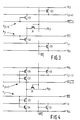
- Figure 3 shows two gate circuits in accordance with the invention which comprise one common transistor.
- the two row selection gates Pj(i-1) and Pji activate the row (i-1) and the row i, respectively, in the memory block j.
- the row selection gate Pji comprises three transistors 31, 32 and 33 which are connected in series between the supply voltages V DD and V ss .
- the transistor 33 is an NMOS transistor and the transistors 31 and 32 are PMOS transistors.
- the row selection signal XSi is applied to the gate of the transistor 32 and the block selection signal BSj is applied to the gates of the transistors 31 and 33.
- the group selection line Lji is connected to the junction of the transistors 32 and 33.
- the group selection line Lji activating the row i in a block j, carries a high signal when the signal BSj is low and the signal XSi is low.
- the signal on the group selection line Lji is low when the signal BSj is high.
- the row selection gate Pj(i-1) is formed by a series connection of the same PMOS transistor 31, the PMOS transistor 22 and the NMOS transistor 23 between supply voltage V DD and V ss , the row selection signal XS(i-1) being applied to the gate of the transistor 22 while the block selection signal BSj is applied to the gate of the transistor 23.
- the group selection line Lj(i-1) is connected to the junction of the transistors 22 and 23.
- the group selection line Lj(i-1) carries a high signal when
- BSj and XS(i-1) are both low.
- Lj(i-1) is discharged and carries a low signal.
- This construction offers the advantages that one PMOS transistor is saved for every two row selection gates and that two neighbouring rows of memory cells in the present lay-out are powered via one voltage line, so that the lay-out becomes smaller and, moreover, the transistor 31 is simply connected to the voltage line V DD , as will be described in detail hereinafter.
- the block selection signal BSj is briefly made “high”, so that the group selection line Lji is discharged. Because the block selection signal BSj is necessarily made “high”, the speed of operation of the memory is slightly reduced. It is another drawback that the group selection lines carry a floating potential after having been discharged in this manner so that, after selection of a group selection line L, the non-selected group selection lines can easily pick up the signals on the selected line L in a capacitive manner, thus causing crosstalk.
- Figure 4 illustrates how these drawbacks are avoided by creating a controlled discharge path for the associated group selection line L by means of a further transistor in each selection gate P.
- an NMOS transistor 34 is arranged with its main electrodes between the group selection line Lji and the second supply source terminal V ss , its gate being connected to the gate of the transistor 32 and to the row selection line XSi.
- the row selection signal XSi is low and the transistor 34 is turned off.
- the row selection signal XSi is high so that the transistor 34 is turned on and the group selection line Lji is discharged.
- the transistor 24 added to the row selection gate Pj(i-1) operates analogously.
- Figure 5 diagrammatically shows a lay-out of a part of the memory circuit in accordance with the invention.
- the memory is constructed by means of a known two-layer metal CMOS technology.
- the bit lines (column selection lines) CA1, CA2, ... CAn in each block, the block selection line BSj and a supply line V ss are realized in the second metal layer (extending vertically in the drawing).
- the row selection lines XS1, ... XS(i-1), XSi, XS(i+1), ... XSm and the supply lines V oo and V ss are realized in the first metal layer (extending horizontally in the drawing) which is isolated from the second metal layer.
- the first and second metal-layer tracks have been partly omitted in Figure 5 in order to illustrate the lay-out of the row selection gates Pji.
- Underneath the first metal layer there are provided polysilicon tracks which form the gates of the various transistors of the row selection gates situated underneath the polysilicon tracks as well as the connections therebetween.
- These polysilicon tracks are denoted by heavily shaded lines in the drawing. The numbering of these tracks refers to the gates of the correspondingly denoted transistors in Figure 4.
- a conductive contact 61 is made between the supply line V DD and the underlying P semiconductor material which forms a first main electrode of the P-channel transistor 31.
- a regular pattern of conductive contacts 62 is provided between the polysilicon track 63 and the block selection line BSj.
- the transistor 31 is a PMOS transistor which is formed in an appropriate N-semiconductor region (denoted by a broken line in the Figure), and so are the PMOS transistors 32 and 22 of the row selection gates Pji and Pj(i-1).
- the NMOS transistors 33 and 34 of the gate Pji are situated together in a P-semiconductor region as denoted by a dotted area. The same holds good for the transistors 23 and 24 of the gate Pj(i-1).
- the gates of the transistors 32 and 34 are connected to the row selection line XSi via the polysilicon line 65i and the gates of the transistors 22 and 24 are connected to the row selection line XS(i-1) via the polysilicon line 65(i-1).
- the group selection line . Lji is served by the gate Pji and is connected to a main electrode of the transistor 32 and to a main electrode of the transistors 33 and 34. The same holds good for the group line Lj(i-1) with respect to the transistors 22, 23 and 24 in the gate Pj(i-1).
- a part of the lay-out is mirror-symmetrical with respect to the contact 61 around which the row selection gates Pj(i-1) and Pji are situated, as well as with respect to the contacts 62, as demonstrated by the polysilicon tracks 73 and 83 which form the gate of an NMOS transistor in the row selection gate Pj(i-2) and the row selection gate Pj(i + 1), respectively.
- the memory cells 90 and 92 are powered via the same contact 61.
Abstract
Description
- The invention relates to an integrated memory circuit which comprises a plurality of memory blocks with memory cells which are arranged in rows and columns, the memory cells which are arranged in a column being. selectable via a column selection line, the memory cells of various memory blocks which are arranged in a row being selectable via a row selection line, a row of memory cells in a memory block being activatable via a logic row selection gate whereto a row selection signal and a block selection signal are applied.
- A memory circuit of this kind is known from ISSCC, Digest of Technical Papers, February 1983, pp. 58-59. The subdivision of a memory into memory blocks with block selection (in the row direction and/or the column direction) is advantageous notably for memories having a capacity of 128 kb and more (256 kb etc.). As a memory is larger, the effect of the capacitance of the bit lines and the word lines will be greater. The charging and discharging of these lines will then be slower. This problem is avoided by subdividing a memory into blocks with selective activation per block. In the known circuit the block selection signal BS and the row selection signal RS are applied to an AND-gate for the selection of a row of memory cells in a memory block. In practice an AND-gate is realized by connecting an inverting amplifier to the output of an inverting AND-gate, so that the circuit becomes large (6 transistors) and slow (due to two gate delays). Another possibility would consist in the selection of a row in a memory block by means of an inverting OR-gate which then receives the inverted block selection signal BS and the inverted row selection signal RS. In the case of CMOS transistors this solution again leads to a slower block selection circuit, because the PMOS transistors must be made wider in order to realize the same power supply as for the AND-gate, so that the input capacitances become higher. The inverting OR-gate switches quickly, but more time will be required for charging these input capacitances. For example, in a 256 kb memory, the block selection signal BS activates a number of 256 (or 512, 1024, depending on the organization of the memory) block selection circuits in parallel.
- It is an object of the invention to realize faster access to a row of memory cells in a memory block.
- To achieve this, an integrated memory circuit in accordance with the-invention is characterized in that a row selection gate comprises at least three transistors, a first main electrode of a first transistor being connected to a first supply source terminal, a second main electrode of said first transistor being connected to a first main electrode of a second transistor, a second main electrode of said second transistor being connected to a first main electrode of a third transistor, a second main electrode of said third transistor being connected to a second supply source terminal, the gate of said second transistor receiving the row selection signal, said first and third transistors being of a different conductivity type and receiving the block selection signal on their gates, a group selection line for activating a row of memory cells in a block being connected to the junction of said second and third transistors, two logic row selection gates for two neighbouring rows of memory cells within the same memory block having a common first transistor.
- The preferred embodiment of an integrated memory circuit with CMOS transistors in accordance with the invention is characterized in that a row selection gate comprises a fourth transistor whose main electrodes are connected to those of the third transistor in the relevant row selection gate, the fourth transistor being of the NMOS type and having its gate connected to the gate of the second transistor in the relevant row selection gate.
- Some advantages of this embodiment consist in that per gate fewer transistors are required in comparison with the AND-gates and OR-gates described above, in that the gates can be simply connected to a Voo supply line and also in that two rows of memory cells can be powered by means of one supply line VDD, which results in a smaller lay-out. Said fourth transistor provides faster access to the meory circuit, as will be described hereinafter.
- The invention will be described in detail hereinafter with reference to the accompanying diagrammatic drawings. Therein:
- Figure 1 shows a memory circuit incorporating block selection in accordance with the invention;
- Figure 2 shows a detail of a memory block as shown in Figure 1;
- Figure 3 shows two gate circuits comprising one common transistor for a memory block as shown in Figure 2;
- Figure 4 shows the preferred embodiment of the gate circuit shown in Figure 3, and
- Figure 5 shows a lay-out of the preferred embodiment of a gate circuit in accordance with the invention.
- Figure 1 shows a
memory circuit 10 whose memory section is subdivided into eightmemory blocks 1 to 8 . Each memory block comprises memory cells which are arranged in rows and columns and which can be selected by means of a column address CA and a row address RA. The row address is applied to arow decoding circuit 11 , and a first part of the column address CA is applied tocolumn address circuits block selection circuit 13, a memory cell in a memory block being selectable by means of the address CA and RA, as will be explained hereinafter. As appears from Figure 1, a memory cell is selected by means of the row andcolumn decoding circuits block selection circuits 13 which apply the block selection signals BS1 to BS8 to thememory blocks 1 to 8, respectively. The meaning of such addressing in a memory circuit will be described with reference to Figure 2. - Figure 2 shows a detail of the memory circuit of Figure 1. The
memory blocks block 1, therow 1 of memory cells is denoted by thereference 1 c1. The first cell of this row is denoted as 1c11, the second cell as 1 c12, etc. The same code is used for the cells and rows in the further memory blocks. A memory cell in a block is selected as follows: via the column lines CA1 or CA2 or ... CAn, one column in each block is activated. The lines CA1 in each block can be driven by the same circuit, but can altematively be driven by a separate buffer. The selection of a row of memory cells in a block is performed by means of a selection gate P which receives a row selection signal via the row selection line XS1 or XS2 or ... XSm for this purpose. Hereinafter, the same notation will be used for a signal and its supply line. The selection gate P in the memory block j (1 ≤ j ≤ 8) and in the row i of the memory block j is denoted as Pji. Furthermore, the inverted block selection signal BSj is applied to the selection gate Pji. Because the row selection circuit XSi need not activate all memory cells of allrows 1 ci, 2ci, ... 8ci (1 5 i ≤ m), but only a number of (eight) selection gates P, essentially faster activation of a row i in a block j and a lower power consumption are achieved. Because the memory comprises a large number of such logic selection gates P, i.e. one gate per row per memory block, the surface area of these selection gates should not be (excessively) large. According to the present state of the art, these gates are formed by AND-gates composed of six transistors in CMOS technology. This gate circuit requires a large integration surface area. A selection gate in an integrated memory circuit in accordance with the invention, however, requires a much smaller surface area and comprises substantially fewer transistors as appears from Figure 3. Figure 3 shows two gate circuits in accordance with the invention which comprise one common transistor. The two row selection gates Pj(i-1) and Pji activate the row (i-1) and the row i, respectively, in the memory block j. The row selection gate Pji comprises threetransistors transistor 33 is an NMOS transistor and thetransistors transistor 32 and the block selection signal BSj is applied to the gates of thetransistors transistors - The row selection gate Pj(i-1) is formed by a series connection of the
same PMOS transistor 31, thePMOS transistor 22 and theNMOS transistor 23 between supply voltage VDD and Vss, the row selection signal XS(i-1) being applied to the gate of thetransistor 22 while the block selection signal BSj is applied to the gate of thetransistor 23. The group selection line Lj(i-1) is connected to the junction of thetransistors - BSj and XS(i-1) are both low. When BSj is high, Lj(i-1) is discharged and carries a low signal.
- This construction offers the advantages that one PMOS transistor is saved for every two row selection gates and that two neighbouring rows of memory cells in the present lay-out are powered via one voltage line, so that the lay-out becomes smaller and, moreover, the
transistor 31 is simply connected to the voltage line VDD, as will be described in detail hereinafter. - It is to be noted that, after each selection of a memory cell and before a next selection of a memory cell in another row within the same memory block, the block selection signal BSj is briefly made "high", so that the group selection line Lji is discharged. Because the block selection signal BSj is necessarily made "high", the speed of operation of the memory is slightly reduced. It is another drawback that the group selection lines carry a floating potential after having been discharged in this manner so that, after selection of a group selection line L, the non-selected group selection lines can easily pick up the signals on the selected line L in a capacitive manner, thus causing crosstalk. Figure 4 illustrates how these drawbacks are avoided by creating a controlled discharge path for the associated group selection line L by means of a further transistor in each selection gate P. To this end, in the row selection gate Pji an
NMOS transistor 34 is arranged with its main electrodes between the group selection line Lji and the second supply source terminal Vss, its gate being connected to the gate of thetransistor 32 and to the row selection line XSi. When a memory cell in row i of block j is selected, the row selection signal XSi is low and thetransistor 34 is turned off. When a row other than the row i is selected, the row selection signal XSi is high so that thetransistor 34 is turned on and the group selection line Lji is discharged. Thetransistor 24 added to the row selection gate Pj(i-1) operates analogously. - Figure 5 diagrammatically shows a lay-out of a part of the memory circuit in accordance with the invention. The memory is constructed by means of a known two-layer metal CMOS technology. The bit lines (column selection lines) CA1, CA2, ... CAn in each block, the block selection line BSj and a supply line Vss are realized in the second metal layer (extending vertically in the drawing). The row selection lines XS1, ... XS(i-1), XSi, XS(i+1), ... XSm and the supply lines Voo and Vss are realized in the first metal layer (extending horizontally in the drawing) which is isolated from the second metal layer. The first and second metal-layer tracks have been partly omitted in Figure 5 in order to illustrate the lay-out of the row selection gates Pji. Underneath the first metal layer there are provided polysilicon tracks which form the gates of the various transistors of the row selection gates situated underneath the polysilicon tracks as well as the connections therebetween. These polysilicon tracks are denoted by heavily shaded lines in the drawing. The numbering of these tracks refers to the gates of the correspondingly denoted transistors in Figure 4. A conductive contact 61 is made between the supply line VDD and the underlying P semiconductor material which forms a first main electrode of the P-
channel transistor 31. A regular pattern ofconductive contacts 62 is provided between the polysilicon track 63 and the block selection line BSj. At the area of the contact 61 the polysilicon track 63 forms the gate of thetransistor 31. Thetransistor 31 is a PMOS transistor which is formed in an appropriate N-semiconductor region (denoted by a broken line in the Figure), and so are thePMOS transistors NMOS transistors transistors transistors transistors transistor 32 and to a main electrode of thetransistors transistors - In order to utilize the same contacts as much as possible, a part of the lay-out is mirror-symmetrical with respect to the contact 61 around which the row selection gates Pj(i-1) and Pji are situated, as well as with respect to the
contacts 62, as demonstrated by the polysilicon tracks 73 and 83 which form the gate of an NMOS transistor in the row selection gate Pj(i-2) and the row selection gate Pj(i + 1), respectively. Thememory cells 90 and 92 are powered via the same contact 61. - Even though the foregoing description concerns only a subdivision in the direction of the rows (each row selection line is actually replaced by a number of row selection lines in the various blocks), a similar subdivision could be made in the direction of the columns. Identical selection gates could then be used.
Claims (9)
Applications Claiming Priority (2)
| Application Number | Priority Date | Filing Date | Title |
|---|---|---|---|
| NL8602178 | 1986-08-27 | ||
| NL8602178A NL8602178A (en) | 1986-08-27 | 1986-08-27 | INTEGRATED MEMORY CIRCUIT WITH BLOCK SELECTION. |
Publications (2)
| Publication Number | Publication Date |
|---|---|
| EP0257680A1 true EP0257680A1 (en) | 1988-03-02 |
| EP0257680B1 EP0257680B1 (en) | 1992-06-10 |
Family
ID=19848464
Family Applications (1)
| Application Number | Title | Priority Date | Filing Date |
|---|---|---|---|
| EP87201432A Expired - Lifetime EP0257680B1 (en) | 1986-08-27 | 1987-07-24 | Integrated memory circuit utilizing block selection |
Country Status (7)
| Country | Link |
|---|---|
| US (1) | US4849943A (en) |
| EP (1) | EP0257680B1 (en) |
| JP (1) | JP2602508B2 (en) |
| KR (1) | KR960001782B1 (en) |
| DE (1) | DE3779705T2 (en) |
| IE (1) | IE60222B1 (en) |
| NL (1) | NL8602178A (en) |
Cited By (2)
| Publication number | Priority date | Publication date | Assignee | Title |
|---|---|---|---|---|
| EP0352745A2 (en) * | 1988-07-28 | 1990-01-31 | Hitachi, Ltd. | Microprocessor |
| GB2259383A (en) * | 1991-08-14 | 1993-03-10 | Samsung Electronics Co Ltd | Block selection in semiconductor memory devices |
Families Citing this family (21)
| Publication number | Priority date | Publication date | Assignee | Title |
|---|---|---|---|---|
| KR910008099B1 (en) * | 1988-07-21 | 1991-10-07 | 삼성반도체통신주식회사 | Power and signal line bussing method for memory device |
| US5278802A (en) * | 1988-10-28 | 1994-01-11 | Texas Instruments Incorporated | Decoding global drive/boot signals using local predecoders |
| JPH0772991B2 (en) * | 1988-12-06 | 1995-08-02 | 三菱電機株式会社 | Semiconductor memory device |
| US5184321A (en) * | 1988-12-06 | 1993-02-02 | Mitsubishi Denki Kabushiki Kaisha | Semiconductor memory device comprising a plurality of memory arrays with improved peripheral circuit location and interconnection arrangement |
| JPH0659209B2 (en) * | 1989-06-09 | 1994-08-10 | 新エネルギー・産業技術総合開発機構 | Variable-volume fermenter |
| US5195053A (en) * | 1989-08-30 | 1993-03-16 | Nec Corporation | Semiconductor memory device wired to accommodate increased capacity without increasing the size of the semiconductor memory device |
| US5040144A (en) * | 1989-11-28 | 1991-08-13 | Motorola, Inc. | Integrated circuit with improved power supply distribution |
| US5245570A (en) * | 1990-12-21 | 1993-09-14 | Intel Corporation | Floating gate non-volatile memory blocks and select transistors |
| JPH04307495A (en) * | 1991-04-04 | 1992-10-29 | Mitsubishi Electric Corp | Semiconductor storage device |
| KR940003400B1 (en) * | 1991-08-27 | 1994-04-21 | 삼성전자 주식회사 | Semiconductor memory devices |
| IT1253680B (en) * | 1991-08-30 | 1995-08-22 | St Microelectronics Srl | NAND TYPE ROM DECODER |
| JP3108505B2 (en) * | 1992-03-13 | 2000-11-13 | 沖電気工業株式会社 | Decoder circuit |
| US5280447A (en) * | 1992-06-19 | 1994-01-18 | Intel Corporation | Floating gate nonvolatile memory with configurable erasure blocks |
| US5267196A (en) * | 1992-06-19 | 1993-11-30 | Intel Corporation | Floating gate nonvolatile memory with distributed blocking feature |
| US5325336A (en) * | 1992-09-10 | 1994-06-28 | Mitsubishi Denki Kabushiki Kaisha | Semiconductor memory device having power line arranged in a meshed shape |
| US5663923A (en) * | 1995-04-28 | 1997-09-02 | Intel Corporation | Nonvolatile memory blocking architecture |
| US5621690A (en) * | 1995-04-28 | 1997-04-15 | Intel Corporation | Nonvolatile memory blocking architecture and redundancy |
| US5959892A (en) * | 1997-08-26 | 1999-09-28 | Macronix International Co., Ltd. | Apparatus and method for programming virtual ground EPROM array cell without disturbing adjacent cells |
| DE19952258A1 (en) * | 1999-10-29 | 2001-05-10 | Infineon Technologies Ag | Integrated memory with folded bit line structure |
| EP1113368A3 (en) * | 1999-12-27 | 2001-09-26 | Matsushita Electric Industrial Co., Ltd. | Semiconductor integrated circuit with cache |
| US6711646B1 (en) * | 2000-10-20 | 2004-03-23 | Sun Microsystems, Inc. | Dual mode (registered/unbuffered) memory interface |
Citations (2)
| Publication number | Priority date | Publication date | Assignee | Title |
|---|---|---|---|---|
| EP0126784A1 (en) * | 1983-05-25 | 1984-12-05 | Ibm Deutschland Gmbh | Semiconductor memory |
| US4554646A (en) * | 1983-10-17 | 1985-11-19 | Mitsubishi Denki Kabushiki Kaisha | Semiconductor memory device |
Family Cites Families (4)
| Publication number | Priority date | Publication date | Assignee | Title |
|---|---|---|---|---|
| JPS6050796A (en) * | 1983-08-31 | 1985-03-20 | Toshiba Corp | Semiconductor storage device |
| JPS60167188A (en) * | 1984-12-24 | 1985-08-30 | Hitachi Ltd | Semiconductor memory |
| NL8500434A (en) * | 1985-02-15 | 1986-09-01 | Philips Nv | INTEGRATED MEMORY CIRCUIT WITH BLOCK SELECTION. |
| US4729118A (en) * | 1986-03-10 | 1988-03-01 | Texas Instruments Incorporated | On-chip converter to reversibly change memory organization using external signals |
-
1986
- 1986-08-27 NL NL8602178A patent/NL8602178A/en not_active Application Discontinuation
-
1987
- 1987-07-24 DE DE8787201432T patent/DE3779705T2/en not_active Expired - Lifetime
- 1987-07-24 EP EP87201432A patent/EP0257680B1/en not_active Expired - Lifetime
- 1987-07-24 US US07/077,154 patent/US4849943A/en not_active Expired - Lifetime
- 1987-08-24 IE IE225587A patent/IE60222B1/en not_active IP Right Cessation
- 1987-08-24 JP JP62208376A patent/JP2602508B2/en not_active Expired - Lifetime
- 1987-08-24 KR KR87009221A patent/KR960001782B1/en not_active IP Right Cessation
Patent Citations (2)
| Publication number | Priority date | Publication date | Assignee | Title |
|---|---|---|---|---|
| EP0126784A1 (en) * | 1983-05-25 | 1984-12-05 | Ibm Deutschland Gmbh | Semiconductor memory |
| US4554646A (en) * | 1983-10-17 | 1985-11-19 | Mitsubishi Denki Kabushiki Kaisha | Semiconductor memory device |
Non-Patent Citations (1)
| Title |
|---|
| 1986 IEEE INTERNATIONAL SOLID-STATE CIRCUITS CONFERENCE, DIGEST OF TECHNICAL PAPERS, 20th February 1986, 1st edition, pages 202-203,348, IEEE, New York, US; M. SEGAWA et al.: "THPM 16.1: A 18ns 8KW x 9b NMOS SRAM" * |
Cited By (3)
| Publication number | Priority date | Publication date | Assignee | Title |
|---|---|---|---|---|
| EP0352745A2 (en) * | 1988-07-28 | 1990-01-31 | Hitachi, Ltd. | Microprocessor |
| EP0352745A3 (en) * | 1988-07-28 | 1991-03-06 | Hitachi, Ltd. | Microprocessor |
| GB2259383A (en) * | 1991-08-14 | 1993-03-10 | Samsung Electronics Co Ltd | Block selection in semiconductor memory devices |
Also Published As
| Publication number | Publication date |
|---|---|
| JPS6363193A (en) | 1988-03-19 |
| EP0257680B1 (en) | 1992-06-10 |
| DE3779705T2 (en) | 1993-01-21 |
| KR880003332A (en) | 1988-05-16 |
| KR960001782B1 (en) | 1996-02-05 |
| DE3779705D1 (en) | 1992-07-16 |
| IE872255L (en) | 1988-02-27 |
| US4849943A (en) | 1989-07-18 |
| IE60222B1 (en) | 1994-06-15 |
| JP2602508B2 (en) | 1997-04-23 |
| NL8602178A (en) | 1988-03-16 |
Similar Documents
| Publication | Publication Date | Title |
|---|---|---|
| US4849943A (en) | Integrated memory circuit having a block selection circuit | |
| EP0072845B1 (en) | Memory system having memory cells capable of storing more than two states | |
| US5315541A (en) | Segmented column memory array | |
| US4125854A (en) | Symmetrical cell layout for static RAM | |
| US5933387A (en) | Divided word line architecture for embedded memories using multiple metal layers | |
| JPH06119781A (en) | Semiconductor memory | |
| US4554646A (en) | Semiconductor memory device | |
| US6233176B1 (en) | Programmable semiconductor memory array having series-connected memory cells | |
| US6577521B2 (en) | Memory architecture and decoder addressing | |
| EP0196119A1 (en) | Integrated memory circuit with block selection | |
| US4384347A (en) | Semiconductor memory device | |
| KR0142037B1 (en) | Semiconductor device | |
| US4395646A (en) | Logic performing cell for use in array structures | |
| US7447074B2 (en) | Read-only memory | |
| JPS61267997A (en) | Semiconductor circuit | |
| US4402063A (en) | Flip-flop detector array for minimum geometry semiconductor memory apparatus | |
| US4901285A (en) | High density read-only memory | |
| JPH0817035B2 (en) | Semiconductor memory device | |
| USRE33280E (en) | Semiconductor memory device | |
| EP0118935A1 (en) | Semiconductor device comprising non-volatile storage transistors | |
| EP1170798B1 (en) | Non-volatile memory matrix architecture | |
| US5245566A (en) | Programmable semiconductor | |
| US4984199A (en) | Semiconductor memory cells having common contact hole | |
| EP0803874B1 (en) | Semiconductor memory device | |
| US5986946A (en) | Method and apparatus for reducing row shut-off time in an interleaved-row memory device |
Legal Events
| Date | Code | Title | Description |
|---|---|---|---|
| PUAI | Public reference made under article 153(3) epc to a published international application that has entered the european phase |
Free format text: ORIGINAL CODE: 0009012 |
|
| AK | Designated contracting states |
Kind code of ref document: A1 Designated state(s): DE FR GB IT |
|
| 17P | Request for examination filed |
Effective date: 19880829 |
|
| 17Q | First examination report despatched |
Effective date: 19900727 |
|
| GRAA | (expected) grant |
Free format text: ORIGINAL CODE: 0009210 |
|
| AK | Designated contracting states |
Kind code of ref document: B1 Designated state(s): DE FR GB IT |
|
| REF | Corresponds to: |
Ref document number: 3779705 Country of ref document: DE Date of ref document: 19920716 |
|
| ITF | It: translation for a ep patent filed |
Owner name: ING. C. GREGORJ S.P.A. |
|
| ET | Fr: translation filed | ||
| PLBE | No opposition filed within time limit |
Free format text: ORIGINAL CODE: 0009261 |
|
| STAA | Information on the status of an ep patent application or granted ep patent |
Free format text: STATUS: NO OPPOSITION FILED WITHIN TIME LIMIT |
|
| 26N | No opposition filed | ||
| ITPR | It: changes in ownership of a european patent |
Owner name: CAMBIO RAGIONE SOCIALE;PHILIPS ELECTRONICS N.V. |
|
| REG | Reference to a national code |
Ref country code: FR Ref legal event code: CD |
|
| PGFP | Annual fee paid to national office [announced via postgrant information from national office to epo] |
Ref country code: FR Payment date: 19970722 Year of fee payment: 11 |
|
| REG | Reference to a national code |
Ref country code: FR Ref legal event code: CD |
|
| PG25 | Lapsed in a contracting state [announced via postgrant information from national office to epo] |
Ref country code: FR Free format text: LAPSE BECAUSE OF NON-PAYMENT OF DUE FEES Effective date: 19990331 |
|
| REG | Reference to a national code |
Ref country code: FR Ref legal event code: ST |
|
| REG | Reference to a national code |
Ref country code: GB Ref legal event code: IF02 |
|
| PG25 | Lapsed in a contracting state [announced via postgrant information from national office to epo] |
Ref country code: IT Free format text: LAPSE BECAUSE OF NON-PAYMENT OF DUE FEES;WARNING: LAPSES OF ITALIAN PATENTS WITH EFFECTIVE DATE BEFORE 2007 MAY HAVE OCCURRED AT ANY TIME BEFORE 2007. THE CORRECT EFFECTIVE DATE MAY BE DIFFERENT FROM THE ONE RECORDED. Effective date: 20050724 |
|
| PGFP | Annual fee paid to national office [announced via postgrant information from national office to epo] |
Ref country code: GB Payment date: 20060727 Year of fee payment: 20 |
|
| PGFP | Annual fee paid to national office [announced via postgrant information from national office to epo] |
Ref country code: DE Payment date: 20060908 Year of fee payment: 20 |
|
| REG | Reference to a national code |
Ref country code: GB Ref legal event code: 732E |
|
| REG | Reference to a national code |
Ref country code: GB Ref legal event code: 732E |
|
| REG | Reference to a national code |
Ref country code: GB Ref legal event code: PE20 |
|
| PG25 | Lapsed in a contracting state [announced via postgrant information from national office to epo] |
Ref country code: GB Free format text: LAPSE BECAUSE OF EXPIRATION OF PROTECTION Effective date: 20070723 |