EP0256494B1 - Activatable conductive links for semiconductor devices - Google Patents
Activatable conductive links for semiconductor devices Download PDFInfo
- Publication number
- EP0256494B1 EP0256494B1 EP87111603A EP87111603A EP0256494B1 EP 0256494 B1 EP0256494 B1 EP 0256494B1 EP 87111603 A EP87111603 A EP 87111603A EP 87111603 A EP87111603 A EP 87111603A EP 0256494 B1 EP0256494 B1 EP 0256494B1
- Authority
- EP
- European Patent Office
- Prior art keywords
- conductive
- insulating layer
- void
- aluminium
- layer
- Prior art date
- Legal status (The legal status is an assumption and is not a legal conclusion. Google has not performed a legal analysis and makes no representation as to the accuracy of the status listed.)
- Expired - Lifetime
Links
Images


Classifications
-
- H—ELECTRICITY
- H01—ELECTRIC ELEMENTS
- H01L—SEMICONDUCTOR DEVICES NOT COVERED BY CLASS H10
- H01L21/00—Processes or apparatus adapted for the manufacture or treatment of semiconductor or solid state devices or of parts thereof
- H01L21/02—Manufacture or treatment of semiconductor devices or of parts thereof
- H01L21/04—Manufacture or treatment of semiconductor devices or of parts thereof the devices having at least one potential-jump barrier or surface barrier, e.g. PN junction, depletion layer or carrier concentration layer
- H01L21/18—Manufacture or treatment of semiconductor devices or of parts thereof the devices having at least one potential-jump barrier or surface barrier, e.g. PN junction, depletion layer or carrier concentration layer the devices having semiconductor bodies comprising elements of Group IV of the Periodic System or AIIIBV compounds with or without impurities, e.g. doping materials
- H01L21/28—Manufacture of electrodes on semiconductor bodies using processes or apparatus not provided for in groups H01L21/20 - H01L21/268
-
- H—ELECTRICITY
- H01—ELECTRIC ELEMENTS
- H01L—SEMICONDUCTOR DEVICES NOT COVERED BY CLASS H10
- H01L23/00—Details of semiconductor or other solid state devices
- H01L23/52—Arrangements for conducting electric current within the device in operation from one component to another, i.e. interconnections, e.g. wires, lead frames
- H01L23/522—Arrangements for conducting electric current within the device in operation from one component to another, i.e. interconnections, e.g. wires, lead frames including external interconnections consisting of a multilayer structure of conductive and insulating layers inseparably formed on the semiconductor body
- H01L23/525—Arrangements for conducting electric current within the device in operation from one component to another, i.e. interconnections, e.g. wires, lead frames including external interconnections consisting of a multilayer structure of conductive and insulating layers inseparably formed on the semiconductor body with adaptable interconnections
- H01L23/5252—Arrangements for conducting electric current within the device in operation from one component to another, i.e. interconnections, e.g. wires, lead frames including external interconnections consisting of a multilayer structure of conductive and insulating layers inseparably formed on the semiconductor body with adaptable interconnections comprising anti-fuses, i.e. connections having their state changed from non-conductive to conductive
- H01L23/5254—Arrangements for conducting electric current within the device in operation from one component to another, i.e. interconnections, e.g. wires, lead frames including external interconnections consisting of a multilayer structure of conductive and insulating layers inseparably formed on the semiconductor body with adaptable interconnections comprising anti-fuses, i.e. connections having their state changed from non-conductive to conductive the change of state resulting from the use of an external beam, e.g. laser beam or ion beam
-
- H—ELECTRICITY
- H01—ELECTRIC ELEMENTS
- H01L—SEMICONDUCTOR DEVICES NOT COVERED BY CLASS H10
- H01L23/00—Details of semiconductor or other solid state devices
- H01L23/52—Arrangements for conducting electric current within the device in operation from one component to another, i.e. interconnections, e.g. wires, lead frames
-
- H—ELECTRICITY
- H01—ELECTRIC ELEMENTS
- H01L—SEMICONDUCTOR DEVICES NOT COVERED BY CLASS H10
- H01L2924/00—Indexing scheme for arrangements or methods for connecting or disconnecting semiconductor or solid-state bodies as covered by H01L24/00
- H01L2924/0001—Technical content checked by a classifier
- H01L2924/0002—Not covered by any one of groups H01L24/00, H01L24/00 and H01L2224/00
-
- Y—GENERAL TAGGING OF NEW TECHNOLOGICAL DEVELOPMENTS; GENERAL TAGGING OF CROSS-SECTIONAL TECHNOLOGIES SPANNING OVER SEVERAL SECTIONS OF THE IPC; TECHNICAL SUBJECTS COVERED BY FORMER USPC CROSS-REFERENCE ART COLLECTIONS [XRACs] AND DIGESTS
- Y10—TECHNICAL SUBJECTS COVERED BY FORMER USPC
- Y10S—TECHNICAL SUBJECTS COVERED BY FORMER USPC CROSS-REFERENCE ART COLLECTIONS [XRACs] AND DIGESTS
- Y10S148/00—Metal treatment
- Y10S148/093—Laser beam treatment in general
Definitions
- This invention relates to activatable conductive links for integrated circuit (IC) semiconductor devices, more particularly to an activatable conductive link disposed between electrically insulated metallic conductive wirings formed in an IC and activatable to establish a conducting path between the wirings when necessary.
- IC integrated circuit
- An activatable conductive link is disposed between conductive wirings which are insulated from each other. Although called a conductive link, the link is initially electrically insulative but can be converted to a conductive condition, when required, by the application of an activating operation thereto.
- Activatable conductive links are frequently used in cooperation with fuses in IC devices such as programmable read only memories, gate arrays and the like, which are fabricated using a master slice system.
- circuit blocks previously formed therein are selectively connected to each other or disconnected from each other using the conductive links or fuses which are activated (put into operation) by irradiation with an energy beam, usually a laser beam.
- Redundancy is implemented by providing an IC, such as a memory chip, with spare circuitry such as spare rows or spare columns for memory cells which are tested after the final fabrication step thereof is finished. Thereafter, bad circuitry is selectively rejected by disconnecting the relevant wirings by blowing previously formed relevant fuses, and is replaced by spare circuitry by activating relevant previously formed conductive links.
- An example of such redundancy technology is reported by James B. Binton on pages 39 and 40 of Electronics, July 28, 1981, in which example conductive pathways (links) of metal-silicon alloy are selectively activated by the irradiation of an argon laser beam between metal layers.
- One activatable conductive link currently in use will be described in relation to master slice production of a semiconductor device, wherein basic circuits are formed on a semiconductor substrate in advance, and thereafter complete circuits of various types, combining basic circuits, are formed in accordance with customers' orders, by selectively changing interconnecting wirings between the basic circuits.
- the polysilicon element 4 is required to be changed to a conductive condition.
- the element 4 is irradiated by a continuous wave laser beam.
- phosphorus dopants contained in the high doped portions 4a of the element 4 are diffused into the non-doped portion 4b, changing that portion 4b into a conductive portion, thus activating the element 4 as a conductive element.
- the areas taken up by conductive links or fuses on chips are required to be as small as possible.
- the above-described activatable conductive element 4 occupies a considerable area on the substrate 1, reducing integration density, and its formation involves complicated fabrication steps.
- IBM Technical Disclosure Bulletin Vol. 21, No. 1, June 1978, page 268, and Vol.21, No.3, August 1978, page 1027 discloses a structure which provides that one laser shot can make a connection between two conductive lines on a silicon dioxide layer.
- the lines end in two closely juxtaposed but initially separated lands.
- Directly over these lands and under the silicon dioxide layer is a metal square.
- the two lands in the square form the laser target. When the target is hit by the laser beam the two lands are welded to the metal square to connect the lines.
- an activatable conductive link structure in a semiconductor device comprising in its non-activated, non-conductive, configuration, a void in an insulating layer of the semiconductor device across which void conductive parts of the device confront one another, the void being such that conductive material does not extend to such an extent, on inner walls of the void as to establish conductive connection between the conductive parts, and such that upon activation of the link conductive material of at least one of the confronting conductive parts melts and fills the void to establish a conductive link between the conductive parts.
- a method of forming and activating an activatable conductive link structure in a semiconductor device comprising forming a void in an insulating layer of the device with conductive parts of the device confronting one another across the void, to provide a non-conductive, non-activated link structure, the void being such that conductive material does not extend on inner walls of the void to establish conductive connection between the conductive parts, for example the void having such an aspect ratio, i.e.
- An embodiment of the present invention can provide an activatable conductive link for connecting two aluminium or aluminium alloy wirings, initially insulated from each other, by activating the conductive link.
- An embodiment of the present invention can provide an activatable conductive link for connecting two wirings disposed in a two-layered structure.
- An embodiment of the present invention can provide an activatable conductive link for connecting two wirings of aluminium or aluminium alloy disposed in the same level on an insulating layer.
- the semiconductor device shown in Fig. 2 and Fig. 3 has a two-layered structure; that is, in a portion of the device shown in Fig. 3, two aluminium wirings 8 and 11 are on two levels and have an insulator layer 9 of PSG interposed between them and are thereby electrically insulated from each other.
- the lower aluminium wiring 8 is formed on another insulator layer 7 of silicon dioxide (SiO2) formed over a silicon substrate 6.
- the side wall 10a of the via hole has a cylindrical PSG surface which is electrically insulative, having a high resistance sufficient to maintain the electrical insulation between the two aluminium wirings 8 and 11.
- the side wall 10a may be partially covered by aluminium deposited during an aluminium sputtering deposition process preceding the lithographic patterning of the aluminium wiring 11.
- the above-described electrical insulation is maintained thanks to the high aspect ratio of the via hole 10 and proper selection of an oblique sputtering angle for the aluminium vapour, which creates an effective shadowing effect for the sputtering.
- An isotropic reactive gas etching process is suitable for providing overhanging side walls, as described later.
- Figs. 9(a) to (d) illustrate fabrication and activation of an activatable conductive link in accordance with the first embodiment of the present invention.
- the excimer laser employed may be, for example, a pulsed Ar F excimer laser (wavelength: 193 nm), having an energy density of 10 J/cm2 and a pulse width of 15 ns.
- one pulse shot is enough to activate the conductive link 10.
- a laser pulse shot of such high energy density and of such narrow pulse width serves to confine thermal diffusion to a small area in the vicinity of the irradiated target portion, preventing damage due to undesirable temperature increases, such as alloying of aluminium members with adjacent silicon members.
- excimer laser such as Kr F2 excimer lasers (wavelength: 248 nm), Xe excimer lasers (wavelength: 308 nm), are available for use in this field.
- a definitely effective method is to open a via hole after patterning the upper aluminium wiring 11.
- This method is described with reference to Figs. 11.
- an upper aluminium layer 11a, a PSG layer 9, a lower aluminium wiring 8, a silicon dioxide (SiO2) layer 7 and a silicon substrate 6 are laminated as illustrated, formed by conventional semiconductor device fabricating methods.
- the upper aluminium layer 11a is then patterned to form an upper aluminium wiring 11, as shown in Fig. 11(b), including a via hole pattern 10v opened amid the pattern of the upper aluminium wiring 11, at a predetermined location, by employing a mask (not shown).
- the trench 13 plays an important role in the achievement of a reliable connection between the associated aluminium wirings. Melted aluminium flows into the trench, filling up the trench 13 and planarizing the cut portion between the wirings. The resulting connection is strong and stable. Without the trench 13, aluminium at the connecting point would overflow in the vicinity of the laser pulse irradiated portion, resulting in an unreliable connection between the wirings to be connected.
- the first conductive path may be made of metal, for example aluminium or aluminium alloy.
- the via hole may be a circular hole having an aspect ratio which is defined as a ratio of the depth to the inner diameter, higher than 1.0.
- the side wall of the via hole may be overhanging.
- the second conductive path may be a conductive doped region formed in a semiconductor substrate of said semiconductor device.
- the first conductive path and said second conductive path may be formed on said first insulating layer in the same level, said concaved portion being a trench having an insulative side wall and a mouth edge of which is in contact with said first conductive path and said second conductive path at mutually facing portions of said mouth edge.
- the first conductive path and said second conductive path may be arranged on said first insulating layer in the same level, said concaved portion being a trench having an insulative side wall.
- a conducting link disposed in an insulating layer of a semiconductor device in combination with a plurality of wirings of the device which are electrically separated from each other.
- the conductive link is selectively activated, providing the wirings with a conducting path, and is activatable by melting metal contained in the wirings by irradiating the portion in the vicinity of the link with a shot of a pulse of laser beam.
- the link comprises a via hole or a trench disposed in the insulating layer depending on the structural configuration of the device. The method of fabricating and activating the conductive link is provided.
Description
- This invention relates to activatable conductive links for integrated circuit (IC) semiconductor devices, more particularly to an activatable conductive link disposed between electrically insulated metallic conductive wirings formed in an IC and activatable to establish a conducting path between the wirings when necessary.
- An activatable conductive link is disposed between conductive wirings which are insulated from each other. Although called a conductive link, the link is initially electrically insulative but can be converted to a conductive condition, when required, by the application of an activating operation thereto.
- Activatable conductive links are frequently used in cooperation with fuses in IC devices such as programmable read only memories, gate arrays and the like, which are fabricated using a master slice system. In these ICs, in accordance with a customer's order, circuit blocks previously formed therein are selectively connected to each other or disconnected from each other using the conductive links or fuses which are activated (put into operation) by irradiation with an energy beam, usually a laser beam.
- As the degree of integration of ICs grows, the necessity for the provision of redundancy within IC chips increases in order to enhance production yield of IC devices. Redundancy is implemented by providing an IC, such as a memory chip, with spare circuitry such as spare rows or spare columns for memory cells which are tested after the final fabrication step thereof is finished. Thereafter, bad circuitry is selectively rejected by disconnecting the relevant wirings by blowing previously formed relevant fuses, and is replaced by spare circuitry by activating relevant previously formed conductive links. An example of such redundancy technology is reported by James B. Binton on pages 39 and 40 of Electronics, July 28, 1981, in which example conductive pathways (links) of metal-silicon alloy are selectively activated by the irradiation of an argon laser beam between metal layers.
- One activatable conductive link currently in use will be described in relation to master slice production of a semiconductor device, wherein basic circuits are formed on a semiconductor substrate in advance, and thereafter complete circuits of various types, combining basic circuits, are formed in accordance with customers' orders, by selectively changing interconnecting wirings between the basic circuits.
- Fig. 1 is a cross-sectional view, illustrating a conductive link for changing interconnecting wirings. 1 is silicon substrate, 2 is a silicon dioxide (SiO₂) layer formed on the
silicon substrate 1, 3 is a phospho-silicate-glass (PSG) layer formed as an insulating layer interposed between the associated layers, 4 is an activatable conductive element made of polycrystalline silicon (polysilicon), and 5 is an aluminium layer. Portions 4a of the polysilicon of the activatable conductive element 4 which contact thealuminium layer 5 are highly doped with phosphorous dopants, having a low electrical resistance, but a centre portion 4b of the element 4 is non-doped, having high electrical resistance. - It will be assumed that in order to set up a required complete circuit system, the polysilicon element 4 is required to be changed to a conductive condition. To achieve this, the element 4 is irradiated by a continuous wave laser beam. As a result, phosphorus dopants contained in the high doped portions 4a of the element 4 are diffused into the non-doped portion 4b, changing that portion 4b into a conductive portion, thus activating the element 4 as a conductive element.
- With regard to the need for high integration packing density of ICs, the areas taken up by conductive links or fuses on chips are required to be as small as possible. The above-described activatable conductive element 4 occupies a considerable area on the substrate 1, reducing integration density, and its formation involves complicated fabrication steps.
- IBM Technical Disclosure Bulletin Vol. 21, No. 1, June 1978, page 268, and Vol.21, No.3, August 1978, page 1027 discloses a structure which provides that one laser shot can make a connection between two conductive lines on a silicon dioxide layer. The lines end in two closely juxtaposed but initially separated lands. Directly over these lands and under the silicon dioxide layer is a metal square. The two lands in the square form the laser target. When the target is hit by the laser beam the two lands are welded to the metal square to connect the lines.
- IEEE Electron Device Letters, Vol. EDL-7, No. 1, January 1986, pages 1 to 4, discusses the planarisation of gold and aluminium thin films using a pulsed laser. Planarisation of films extending over via holes is discussed.
- Attention is also directed to EP-A-0 251 523, which forms part of the state of the art by virtue of Article 54(3) EPC.
- According to the present invention there is provided an activatable conductive link structure in a semiconductor device, the structure comprising in its non-activated, non-conductive, configuration, a void in an insulating layer of the semiconductor device across which void conductive parts of the device confront one another, the void being such that conductive material does not extend to such an extent, on inner walls of the void as to establish conductive connection between the conductive parts, and such that upon activation of the link conductive material of at least one of the confronting conductive parts melts and fills the void to establish a conductive link between the conductive parts.
- According to the present invention there is also provided a method of forming and activating an activatable conductive link structure in a semiconductor device, the method comprising
forming a void in an insulating layer of the device with conductive parts of the device confronting one another across the void, to provide a non-conductive, non-activated link structure, the void being such that conductive material does not extend on inner walls of the void to establish conductive connection between the conductive parts, for example the void having such an aspect ratio, i.e. ratio of depth into the insulating layer to upper opening width, as to prevent deposition of conductive material on its inner walls such as would establish a conductive connection between the conductive parts,
and activating the link structure by locally heating a region in the vicinity of the void such that conductive material of at least one of the conductive parts melts and fills the void to establish a conductive link between the conductive parts. - An embodiment of the present invention can provide an activatable conductive link for connecting two aluminium or aluminium alloy wirings, initially insulated from each other, by activating the conductive link.
- An embodiment of the present invention can provide an activatable conductive link for connecting two wirings disposed in a two-layered structure.
- An embodiment of the present invention can provide an activatable conductive link for connecting two wirings of aluminium or aluminium alloy disposed in the same level on an insulating layer.
- In accordance with an embodiment of the present invention, there is provided a via hole, disposed in an insulator layer formed on a semiconductor substrate, having a high aspect ratio (a ratio of depth to inner diameter). Two aluminium or aluminium alloy wirings are formed respectively on the top and at the bottom surfaces of the insulator layer, being electrically insulated from each other by the insulating layer. The via hole has an electrically insulating side wall, electrically insulating and physically connecting the two wirings. If the connection of the two stacked aluminium wirings is required, a portion of an aluminium wiring in the vicinity of the via hole is irradiated by a shot of high energy excimer laser beam pulse irradiated from the top side. The aluminium included in the irradiated portion of the aluminium wiring is melted, being introduced into the via hole, and filling up the via hole. Thus, the via hole is changed to be conductive. The via hole acts as an activatable conductive link between the stacked aluminium wirings.
- In a similar manner, another embodiment of the invention provides a trench or slot having a high aspect ratio (ratio of depth to lateral width) disposed in an insulator layer formed on a substrate of a semiconductor device such as an IC, the trench or slot intercepting an aluminium wiring formed on the insulator layer. The aluminium wiring is cut into two, forming two wirings which are electrically insulated from each other by the step portions (side walls) of the trench where the insulating layer is exposed. If the connection of the two aluminium wirings is required, the trench is filed up with melted aluminium by a shot of an excimer laser pulse in a similar manner to that described above, thus making the trench conductive. The trench, therefore, acts as an activatable conductive link for connecting two portions of conductive members placed in the same level.
- Conductive links in accordance with the present invention can be particularly effectively employed in relation to master slice semiconductor device processes. The conductive links are small, on the order of µm, occupying a small substrate area of a device, and thus facilitating achievement of high density integration.
- Reference is made, by way of example, to the accompanying drawings, in which:-
- Fig. 1 is a cross-sectional view illustrating the structure of a previous conducting link;
- Fig. 2 is a perspective view illustrating the structure of a conductive link in accordance with a first embodiment of the present invention;
- Fig. 3 is a cross-sectional view of the conductive link of Fig. 2, taken along line A-A;
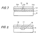
- Fig. 4 is a cross-sectional view of a modified version of the conductive link of Fig. 2, including a via hole having an overhanging side wall;
- Fig. 5 is a perspective view illustrating the structure of a conductive link in accordance with a second embodiment of the present invention;
- Fig. 6 is a cross-sectional view of the conductive link of Fig. 5, taken along line B-B;
- Fig. 7 is a cross-sectional view of a modified version of the conductive link of Fig. 5, including a trench having an overhanging side wall;
- Fig. 8 is a cross-sectional view illustrating the structure of a conductive link in accordance with a third embodiment of the present invention;
- Figs. 9(a) to 9(d) are respective cross-sectional views illustrating fabrication and activation of a conductive link in accordance with the first embodiment of the present invention;
- Figs. 10(a) to 10(d) are respective cross-sectional views illustrating fabrication and activation of a conductive link in accordance with the second embodiment of the present invention;
- Figs. 11(a) to 11(d) are respective cross-sectional views illustrating fabrication and activation of a conductive link in accordance with the first embodiment of the present invention; and
- Figs. 12(a) to 12(d) are respective cross-sectional views illustrating fabrication and activation steps of a conductive link in accordance with the second embodiment of the present invention.
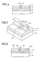
- Figs. 2 is a perspective view of a part of a semiconductor device, partially broken away to reveal a structure, in accordance with a first embodiment of the present invention, providing an activatable conductive link (a via hole) for linking two aluminium wirings arranged in a two-layered structure and separated by a phosphorous silicate glass (PSG) layer. Fig. 3 is a cross-sectional view of the structure of Fig. 2, taken along line A-A shown in Fig. 2.
- The semiconductor device shown in Fig. 2 and Fig. 3, has a two-layered structure; that is, in a portion of the device shown in Fig. 3, two
aluminium wirings insulator layer 9 of PSG interposed between them and are thereby electrically insulated from each other. Thelower aluminium wiring 8 is formed on anotherinsulator layer 7 of silicon dioxide (SiO₂) formed over asilicon substrate 6. Avia hole 10 having a high aspect ratio (depth/diameter ratio), with a small diameter of 0.9 µm, and a large depth of 1.2 µm, for example, is disposed in a direction approximately normal to the principal plane of thesubstrate 6, physically extending between the upper andlower aluminium wirings lower mouths via hole 10 respectively open onto or within theupper wiring 11 and thelower wiring 8. Theside wall 10a of the via hole has a cylindrical PSG surface which is electrically insulative, having a high resistance sufficient to maintain the electrical insulation between the twoaluminium wirings - As will be described later, when the via
hole 10 is opened in thePSG layer 9 before the formation of theupper aluminium wiring 11, theside wall 10a may be partially covered by aluminium deposited during an aluminium sputtering deposition process preceding the lithographic patterning of thealuminium wiring 11. However, the above-described electrical insulation is maintained thanks to the high aspect ratio of the viahole 10 and proper selection of an oblique sputtering angle for the aluminium vapour, which creates an effective shadowing effect for the sputtering. Furthermore, it is desirable for the viahole 10 to have overhangingside walls 10d, in order to achieve a more effective shadowing effect, as illustrated in the cross-sectional view of Fig. 4. An isotropic reactive gas etching process is suitable for providing overhanging side walls, as described later. - If the via
hole 10 is opened up after formation of theupper aluminium wiring 11, then the above-described problem relating to the electrical insulation power of theside wall 10a is easily solved, although the durability of a mask used for lithographic patterning of the upper aluminium wiring is not high. To overcome this problem an opening having a form corresponding to the mouth of the via hole (or the trench - see below) may be opened in a predetermined portion of the wiring, and thereafter the via hole (or trench) may be formed with the aid of the above-described opening, as described below. - Fig. 5 is a perspective view of a part of a semiconductor device, partially broken away to reveal a structure in accordance with a second embodiment of the present invention, illustrating an activatable conductive link (a trench or a slot) for linking two aluminium wirings arranged on the same level formed on a phosphorous silicate glass (PSG) layer. Fig. 6 is a cross-sectional view of the structure of Fig. 5, taken along line B-B shown in Fig. 5.
- The semiconductor device shown in Fig. 5 and Fig. 6 is a one-layered structure: that is, the aluminium wirings are formed on one level. In the device, a
PSG layer 12, and a silicon dioxide (SiO₂)layer 7 are formed on asilicon substrate 6. In the portion of the device shown in Fig. 6, twoaluminium wirings 14a and 14b have between them atrench 13 formed inPSG layer 12. Bothaluminium wirings 14a and 14b are formed on thePSG layer 12. Thetrench 13 has a small lateral length (width) of 0.9 µm and a large depth of 1.2 µm, for example, having a high aspect ratio of 1.33. Thetrench 13 extends depthwise in a direction approximately normal to the principal plane of thesubstrate 6, physically between, and electrically disconnecting, thealuminium wirings 14a and 14b. The width of the trench separates the wirings. The length of thetrench 13 is shown in Fig. 5 as greater than the width of thealuminium wirings 14a and 14b, so that the edges 13b of the mouth of thetrench 13 extend, longitudinally of the trench, beyond the side edges of thealuminium wirings 14a and 14b, providing a greater tolerance for alignment of thewirings 14a and 14b with thetrench 13, if necessary. Theside wall 13a of the trench has a PSG surface which is electrically insulative, having a high resistance, sufficient to maintain electrical insulation between the twoaluminium wirings 14a and 14b. If thetrench 13 is opened in thePSG layer 12 using an aluminium sputtering deposition, a problem may occur in that theside wall 13a is covered partially and undesirably with aluminium during the aluminium sputtering deposition. However, the problem is not so critical as with the first embodiment described above. This is because at least one of theside walls 13a of thetrench 13, and the bottom surface thereof, are shaded from impinging aluminium vapour during the aluminium sputtering process due to the shadow effect of the aluminium sputtering deposition process. For reasons similar to the first embodiment, thetrench 13 desirably has an overhangingside wall 13d as illustrated in the cross-sectional view of Fig. 7, which can be achieved by employing a reactive gas etching process for forming the trench, as described later. - Fig. 8 is a cross-sectional view illustrating a structure in accordance with a third embodiment of the present invention, which is modified form of the first embodiment, in which the lower aluminium wiring of the first embodiment is replaced by a doped conductive region. In this case, as shown in Fig. 8, a doped
region 16, which is conductive, is formed in asilicon substrate 6 immediately beneath a viahole 17. Analuminium wiring 18 is insulated from the dopedregion 16 by a silicon dioxide (SiO₂)layer 15. The viahole 17 has a high aspect ratio, being capable of acting as a conducting link to connect thealuminium wiring 18 to thedoping region 16 if so required. - In the three above-described embodiments, reference is made to aluminium wirings or aluminium layers. However, in place of aluminium other aluminium alloys such as aluminium silicon alloys and aluminium copper alloys which are conventionally used in semiconductor devices, are also applicable. Further, PSG layers 9 and 12 in the above-described embodiments can be replaced by other insulating, e.g. oxide layers, such as a silicon dioxide (SiO₂) layer, if the use thereof is permitted in the context of the production technology employed for the semiconductor device as a whole.
- Fabrication and activation methods for activatable conductive links embodying the present invention will now be described.
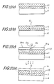
- Figs. 9(a) to (d) illustrate fabrication and activation of an activatable conductive link in accordance with the first embodiment of the present invention.
- Fig. 9(a) shows a stage reached after a silicon dioxide (SiO₂)
layer 7 is formed over a silicon (Si)substrate 6, a lower aluminium layer is formed over thesilicon dioxide layer 7, and subsequently, the lower aluminium layer is patterned to form alower aluminium wiring 8. Further, aPSG layer 9 is formed over thealuminium wiring 8 and the silicon dioxide (SiO₂) layer. Thus a laminated structure is formed as shown in Fig. 9(a). This structure can be formed by conventional technology used in this field. To the laminated structure of Fig. 9(a), the following steps are applied in sequence: - (1) A via
hole 10 is opened in thePSG layer 9, at a specified portion thereof, having a depth sufficient to reach the underlyinglower aluminium wiring 8. The aspect ratio (depth/diameter ratio) of the viahole 10 is taken higher than 1.0. The viahole 10 can be opened by a conventional reactive ion etching method, which is an anisotropic etching method and is suitable for substantially precise patterning. - (2) Then, over the upper surface of the structure, aluminium is sputtered to form an upper aluminium layer, which is patterned thereafter to form an
upper wiring 11. For this, thestructure 6 is placed in a reaction chamber of an aluminium sputtering deposition apparatus (not shown) spaced from the source of aluminium vapour such that aluminium vapour impinges onto the structure obliquely, providing a shadow effect for the viahole 10 to ensure that a PSG side wall surface of the viahole 10 is uncovered by aluminium. Consequently, electrical insulation between the upper aluminium layer and thelower aluminium wiring 8 is assured. The angle of the direction of sputtering of aluminium vapour to the normal to the principal plane of thePSG layer 9 should be properly selected depending on the aspect ratio of the viahole 10. In the resulting structural configuration, thelower aluminium wiring 8 and the upper aluminium layer are still electrically insulated from each other. Subsequently, the upper aluminium layer is patterned in a conventional manner to form anupper aluminium wiring 11 as shown in Fig. 9(c). - (3) Thereafter, when electrical connection between the
upper aluminium wiring 11 and thelower aluminium 8 is required, thealuminium layer 11 is irradiated from above with an excimer laser pulse spot of high energy and narrow pulse width, as indicated by arrows L in Fig. 9(d). The irradiated portion of theupper aluminium wiring 11 is instantaneously melted. The melted aluminium flows into the viahole 10, filling it up completely. As a result, thealuminium wiring 11 and thealuminium wiring 8 are electrically connected. The connection is substantially stable and reliable. - The excimer laser employed may be, for example, a pulsed Ar F excimer laser (wavelength: 193 nm), having an energy density of 10 J/cm² and a pulse width of 15 ns. In this case, one pulse shot is enough to activate the
conductive link 10. A laser pulse shot of such high energy density and of such narrow pulse width serves to confine thermal diffusion to a small area in the vicinity of the irradiated target portion, preventing damage due to undesirable temperature increases, such as alloying of aluminium members with adjacent silicon members. - A low laser beam energy density, below 3 J/cm², is not effective to melt the aluminium of the relevant aluminium wirings instantaneously, and a high energy density, over 15 J/cm², is harmful in that
aluminium wirings range 5 to 12 J/cm² is desirable for practical use. - A longer pulse (having a width of 1µs, for example), or a continuous laser beam, may also cause damage, and not be suitable for practical use.
- Other kinds of excimer laser, such as Kr F₂ excimer lasers (wavelength: 248 nm), Xe excimer lasers (wavelength: 308 nm), are available for use in this field.
- A method for fabricating an activatable conductive link in accordance with the second embodiment of the present invention is similar to that for the first embodiment. This method will be described briefly. A laminated structure comprising a
PSG layer 12, a silicon dioxide (SiO₂)layer 7, and asubstrate 6 is formed as illustrated in Fig. 10(a). Then, atrench 13 is opened in a selected portion of thePSG layer 12, employing a conventional reactive ion etching method, as shown in Fig. 10(b). Subsequently, an aluminium layer is formed over thePSG layer 12. Thereafter, the aluminium layer is patterned to formaluminium wirings 14a and 14b which are traversed by thetrench 13 as shown in Fig. 10(c). The subsequent activation of the conductive link is performed in the same manner as for the first embodiment, and further description thereof is omitted here. Fig. 10(d) illustrates the state of the conductive link of the second embodiment after activation. - As already indicated above, it is important to secure a portion of the PSG surface of the side wall (10a, 10d) of the via hole (or
trench - An effective method for securing the insulating capability of the via hole (or trench) is provided by the use of a conventional lift-off process using, for example, photoresist resin. The via hole 10 (or trench) is filled up with the resin in advance, before aluminium deposition over the via hole (or trench), preventing deposition of aluminium on the side wall. Thereafter, the resin is removed from the via hole (or trench).
- Another method, already described above, is to form the via hole (or trench) with overhanging side walls by employing a conventional reactive gas etching method for opening the via hole. The employed etchant gas is a mixture of tetrafluoride carbon (CF₄) and trifluoromethane (CHF₃), for example. Because the etching method is essentially isotropic and the adhesion between a mask (not shown) and the
PSG layer 9 is very strong the resulting via hole is subject to so-called "under etching", which provides overhanging side walls (10d, 13d) as shown in Fig. 4 or Fig. 7, which is effective to provide the side wall with a strong shadow effect during aluminium deposition, with the result that an exposed PSG portion of the side wall is secured. - A definitely effective method is to open a via hole after patterning the
upper aluminium wiring 11. This method is described with reference to Figs. 11. As shown in Fig. 11(a), an upper aluminium layer 11a, aPSG layer 9, alower aluminium wiring 8, a silicon dioxide (SiO₂)layer 7 and asilicon substrate 6 are laminated as illustrated, formed by conventional semiconductor device fabricating methods. The upper aluminium layer 11a is then patterned to form anupper aluminium wiring 11, as shown in Fig. 11(b), including a via hole pattern 10v opened amid the pattern of theupper aluminium wiring 11, at a predetermined location, by employing a mask (not shown). - Then, the
PSG layer 9 immediately beneath the via hole pattern 10v is etched by a conventional reactive ion etching method, or a conventional reactive gas etching method, until the formed hole reaches the underlyinglower aluminium wiring 8. The thus opened viahole 10 has aside wall 10a having an entirely exposed PSG surface. The conductive link is completed as shown in Fig. 11(c). The activating method for this viahole 10 is as described above, and the resulting activated link is shown in Fig. 11(d). - A method of fabricating an activatable conductive link in accordance with the second embodiment of the present invention is similar to that of the first embodiment. The fabricating method thereof, therefore, is described only briefly. A laminated structure comprising an
aluminium layer 14c, aPSG layer 12, a silicon dioxide (SiO₂)layer 7, and asubstrate 6 laminated in the illustrated order is formed as shown in Fig. 12(a). Then, thealuminium layer 14c is patterned to form analuminium wiring 14 including atraversing slit pattern 13v disposed at a position where atrench 13 is to be disposed, as shown in Fig. 12(b). Subsequently, thetrench 13 is opened in thePSG layer 12 below theslit 13v employing a conventional drying etching process, as shown in Fig. 12(c). As a result, thealuminium wiring 14 is traversed by thetrench 13, and separated intoaluminium wirings 14a and 14b as shown in Fig. 12(c). Since the subsequent activation method is the same as that of the first embodiment, further description thereof is omitted. Fig. 12(d) illustrates the state of the conductive link after activation thereof. - With regard to the activation process of a conducting link of the second embodiment, it should be noted that the
trench 13 plays an important role in the achievement of a reliable connection between the associated aluminium wirings. Melted aluminium flows into the trench, filling up thetrench 13 and planarizing the cut portion between the wirings. The resulting connection is strong and stable. Without thetrench 13, aluminium at the connecting point would overflow in the vicinity of the laser pulse irradiated portion, resulting in an unreliable connection between the wirings to be connected. - The method for fabricating a structure in accordance with the third embodiment of the present invention is the same as that of the first embodiment except for the formation in advance of a doped
region 16 in thesubstrate 6. - According to embodiments of the present invention, as described above, an activatable conductive link is formed between two aluminium wirings in a semiconductor device, which are insulated from each other by an insulating layer. The conductive link is formed using a via hole or a trench with a high aspect ratio, disposed in the insulating layer. When necessary, the two aluminium wirings are easily connected using a simple method, namely irradiation with one shot of an excimer laser beam pulse. In addition, the contact area (e.g. the via hole area), occupying a small area on the relevant silicon substrate. The insulating capability of the link before activation thereof, and the conducting capability of the link after activation thereof, are both substantially stable and reliable. As a result, a semiconductor device with a high integration density can be produced in a master slice system with low cost and high reliability.
- The present invention provides and includes within its scope a conducting link, in an integrated semiconductor circuit of a semiconductor device, in combination with a plurality of conductive paths including a first conductive path and a second conducting path which are electrically insulated from each other by an insulating layer, disposed between said conductive paths in a specified portion of the circuit, being selectively activatable to provide a conductive link path between said conductive paths, comprising:
a concaved portion having a high aspect ratio formed in said insulating layer, physically contacting with said first conductive path and said second conductive path, and electrically maintaining the insulation between said first and second conductive paths. - The concaved portion may have a mouth edge which contacts to said first conductive path and said second conductive path at portions thereof separated from each other, and an inside surface which is insulative enough to maintain the electrical insulation between said first and second conductive paths.
- The first conductive path may be made of metal, for example aluminium or aluminium alloy.
- The insulating layer may be a phosphorous silicate glass (PSG) layer or a silicon dioxide (SiO₂) layer.
- The first conductive path and said second conductive path may be arranged in a two-layered arrangement interposed by said insulating layer, said concaved portion being a via hole which has a side wall with insulative surface, and an upper mouth edge and a lower mouth edge respectively physically contacting with said first conductive path and said second conductive path.
- The via hole may be a circular hole having an aspect ratio which is defined as a ratio of the depth to the inner diameter, higher than 1.0.
- The side wall of the via hole may be overhanging.
- The surface of said second conductive path may be exposed at the lower mouth of said via hole.
- The second conducting path may be disposed on an insulating layer over a semiconductor substrate of said semiconductor device.
- The second conductive path may be a conductive doped region formed in a semiconductor substrate of said semiconductor device.
- The first conductive path and said second conductive path may be formed on said first insulating layer in the same level, said concaved portion being a trench having an insulative side wall and a mouth edge of which is in contact with said first conductive path and said second conductive path at mutually facing portions of said mouth edge.
- The trench may have an aspect ratio defined as a ratio of the depth to the lateral width of said trench, higher than 1.0.
- The side wall of said trench may be overhanging.
- The present invention also provides and includes within its scope a method for creating and activating a conducting link, in an integrated semiconductor circuit of a semiconductor device, selectively activatable in combination with a plurality of conducting paths which are electrically insulated from each other by a first insulating layer, said method comprising the steps of:
- (a) forming a concaved portion with a high aspect ratio in said first insulating layer at a specified portion;
- (b) forming a first conductive path of metal such that said first conducting path is electrically insulated by said concaved portion from another second conducting path to which said first conducting path is to be connected; and
- (c) activating said conducting link, when activation is required, by locally heating said concaved portion and a region in the vicinity thereof, melting metal contained in the heated portion of said first conducting path, making the melted metal flow into said concaved portion to fill up said concaved portion with said metal, and thus providing a conductive path between said first and second conductive paths.
- The first conducting path may be made of aluminium or aluminium alloy.
- The local heating may employ an energy beam pulse.
- The energy beam may be an excimer laser beam.
- The energy density of said excimer laser beam is preferably in the 5 J/cm² to 12 J/cm².
- The first conductive path and said second conductive path may be arranged in a two-layered arrangement interposed by said first insulating layer, said concaved portion being a via hole, and said second conductive path being made of aluminium or aluminium alloy formed over an insulating layer formed over a semiconductor substrate, or made of a doped conductive region formed in said semiconductor substrate.
- Process (a) above may comprise, forming said via hole in said first insulator at a specified portion such that said via hole reaches said underlying second conducting path, and
process (b) above may comprise, forming an aluminium or aluminium alloy layer over said second insulating layer including said via hole, and patterning said layer to form said first conductive path in alignment with said via hole, thus creating a conducting link which is in an insulating state. - The first conductive path and said second conductive path may be arranged on said first insulating layer in the same level, said concaved portion being a trench having an insulative side wall.
- In this case process (a) above may comprise, forming said trench in said first insulator at said specified portion,
process (b) above may comprise, forming an aluminium or aluminium alloy layer over said first insulating layer, including said trench, and patterning said layer to form said first and second conductive paths in alignment with said trench such that both of said first and second conductive paths are insulated from each other and are respectively in contact with mutually facing portions of the mouth edge of said trench. - The via hole or trench may be formed in said first insulating layer so as to have overhanging side wall in said via hole or said trench employing an isotropic reactive etching method.
- The present invention further provides and includes within its scope a method for creating and activating a conducting link, in an integrated semiconductor circuit of a semiconductor device, selectively activatable in combination with a plurality of conducting paths which are electrically insulated from each other by a first insulating layer, said method comprising the steps of:
- (a) forming a first conductive path of aluminium or aluminium alloy over said first insulating layer, said first conducting path including a pattern of a mouth of said concaved portion at a specified portion where said conducting link is to be disposed;
- (b) forming a concaved portion with a high aspect ratio in said first insulating layer, utilizing said pattern of the mouth of said concaved portion, at said specified portion such that said first conducting path is electrically insulated by said concaved portion from said second conducting path to which said first conducting path is to be connected; and
- (c) activating said conducting link, when activation is required, by locally heating said concaved portion and a region in the vicinity thereof, melting metal contained in the heated portion of said first conducting path, making the melted metal flow into said concaved portion to fill up said concaved portion with said metal, and thus providing a conductive path between said first and second conductive paths.
- A conducting link disposed in an insulating layer of a semiconductor device in combination with a plurality of wirings of the device which are electrically separated from each other. The conductive link is selectively activated, providing the wirings with a conducting path, and is activatable by melting metal contained in the wirings by irradiating the portion in the vicinity of the link with a shot of a pulse of laser beam. The link comprises a via hole or a trench disposed in the insulating layer depending on the structural configuration of the device. The method of fabricating and activating the conductive link is provided.
Claims (15)
- An activatable conductive link structure in a semiconductor device, the structure comprising in its non-activated, non-conductive, configuration, a void in an insulating layer of the semiconductor device across which void conductive parts of the device confront one another, the void being such that conductive material does not extend to such an extent on inner walls of the void as to establish conductive connection between the conductive parts, and such that upon activation of the link conductive material of at least one of the confronting conductive parts melts and fills the void to establish a conductive link between the conductive parts.
- A structure as claimed in claim 1, wherein at least one of the confronting conductive parts, which melts upon activation, is of metal, for example aluminium or aluminium alloy.
- A structure as claimed in claim 1 or 2, wherein the insulating layer is of phospho silicate glass (PSG) or of silicon dioxide.
- A structure as claimed in claim 1, 2 or 3, wherein the confronting conductive parts are parts of respective conductive layers, one above the insulating layer, one below the insulating layer, or are, respectively, a part of a conductive layer above the insulating layer and a part of a doped conductive device substrate region below the insulating layer, and the void is a via hole through the insulating layer.
- A structure as claimed in claim 1, 2 or 3, wherein the confronting conductive parts are both formed on an upper surface of the insulating layer and the void is a trench, slot or hole in the insulating layer.
- A structure as claimed in any preceding claim, wherein the side walls of the void, defined by material of the insulating layer, are overhanging.
- A structure as claimed in any preceding claim, wherein the void has an aspect ratio, i.e ratio of depth into the insulating layer to upper opening width, of 1.0 or more.
- A method of forming and activating an activatable conductive link structure in a semiconductor device, the method comprising
forming a void in an insulating layer of the device with conductive parts of the device confronting one another across the void, to provide a non-conductive, non-activated link structure, the void being such that conductive material does not extend to such an extent on inner walls of the void as to establish conductive connection between the conductive parts,
and activating the link structure by locally heating a region in the vicinity of the void such that conductive material of at least one of the conductive parts melts and fills the void to establish a conductive link between the conductive parts. - A method as claimed in claim 8, wherein the local heating is accomplished using an energy beam pulse, for example an excimer laser beam pulse.
- A method as claimed in claim 9, wherein an excimer laser beam pulse of energy density in the range 5 J/cm² to 12 J/cm² is employed.
- A method as claimed in any one of claims 8 to 10, wherein the insulating layer is formed over one of the conductive parts, which may belong to a conductive layer or a doped conductive device substrate region, and the other conductive part is part of a conductive layer formed over the insulating layer, the void being formed as a via hole through the insulating layer.
- A method as claimed in any one of claims 8 to 10, wherein the conductive parts are parts of a conductive layer formed over the insulating layer and the void is formed as a trench, slot or hole formed in the insulating layer.
- A method as claimed in any one of claims 8 to 12, wherein the side walls of the void, defined by material of the insulating layer, are formed so as to be overhanging, employing an isotropic reactive etching method.
- A method as claimed in any one of claims 8 to 13, wherein the void in the insulating layer is formed prior to formation of the conductive layer over the insulating layer.
- A method as claimed in any one of claims 8 to 13, wherein the void in the insulating layer is formed after formation of the conductive layer over the insulating layer, using an aperture provided in the conductive layer as a pattern for etching the void into the insulating layer.
Applications Claiming Priority (2)
| Application Number | Priority Date | Filing Date | Title |
|---|---|---|---|
| JP189094/86 | 1986-08-12 | ||
| JP61189094A JPS6344739A (en) | 1986-08-12 | 1986-08-12 | Manufacture of semiconductor device |
Publications (3)
| Publication Number | Publication Date |
|---|---|
| EP0256494A2 EP0256494A2 (en) | 1988-02-24 |
| EP0256494A3 EP0256494A3 (en) | 1988-07-27 |
| EP0256494B1 true EP0256494B1 (en) | 1993-01-07 |
Family
ID=16235236
Family Applications (1)
| Application Number | Title | Priority Date | Filing Date |
|---|---|---|---|
| EP87111603A Expired - Lifetime EP0256494B1 (en) | 1986-08-12 | 1987-08-11 | Activatable conductive links for semiconductor devices |
Country Status (5)
| Country | Link |
|---|---|
| US (1) | US4968643A (en) |
| EP (1) | EP0256494B1 (en) |
| JP (1) | JPS6344739A (en) |
| KR (1) | KR910004038B1 (en) |
| DE (1) | DE3783404T2 (en) |
Families Citing this family (21)
| Publication number | Priority date | Publication date | Assignee | Title |
|---|---|---|---|---|
| US5070392A (en) * | 1988-03-18 | 1991-12-03 | Digital Equipment Corporation | Integrated circuit having laser-alterable metallization layer |
| US5250465A (en) * | 1991-01-28 | 1993-10-05 | Fujitsu Limited | Method of manufacturing semiconductor devices |
| US5451811A (en) * | 1991-10-08 | 1995-09-19 | Aptix Corporation | Electrically programmable interconnect element for integrated circuits |
| US5321322A (en) * | 1991-11-27 | 1994-06-14 | Aptix Corporation | Programmable interconnect architecture without active devices |
| WO1993012582A1 (en) * | 1991-12-13 | 1993-06-24 | Knights Technology, Inc. | Programmable logic device cell and method |
| JPH0799791B2 (en) * | 1992-04-15 | 1995-10-25 | インターナショナル・ビジネス・マシーンズ・コーポレイション | Circuit line connection method on transparent substrate |
| JPH06124913A (en) * | 1992-06-26 | 1994-05-06 | Semiconductor Energy Lab Co Ltd | Laser treatment |
| KR960009996B1 (en) * | 1992-08-24 | 1996-07-25 | 금성일렉트론 주식회사 | Semiconductor repair device |
| US5453402A (en) * | 1992-12-15 | 1995-09-26 | Advanced Micro Devices, Inc. | Selective metal via plug growth technology for deep sub-micrometer ULSI |
| JPH06260441A (en) * | 1993-03-03 | 1994-09-16 | Nec Corp | Manufacture of semiconductor device |
| US5861325A (en) * | 1994-03-10 | 1999-01-19 | Massachusetts Institute Of Technology | Technique for producing interconnecting conductive links |
| US5920789A (en) * | 1994-10-11 | 1999-07-06 | Massachusetts Institute Of Technology | Technique for producing interconnecting conductive links |
| US5585602A (en) * | 1995-01-09 | 1996-12-17 | Massachusetts Institute Of Technology | Structure for providing conductive paths |
| US5940727A (en) * | 1994-10-11 | 1999-08-17 | Massachusetts Institute Of Technology | Technique for producing interconnecting conductive links |
| JPH09510320A (en) * | 1994-03-10 | 1997-10-14 | マサチユセツツ・インスチチユート・オブ・テクノロジー | Method of manufacturing conductive link for connection |
| TW278229B (en) * | 1994-12-29 | 1996-06-11 | Siemens Ag | Fuse structure for an integrated circuit device and method for manufacturing a fuse structure |
| JP3160198B2 (en) * | 1995-02-08 | 2001-04-23 | インターナショナル・ビジネス・マシーンズ・コーポレ−ション | Semiconductor substrate on which decoupling capacitor is formed and method of manufacturing the same |
| US5731047A (en) * | 1996-11-08 | 1998-03-24 | W.L. Gore & Associates, Inc. | Multiple frequency processing to improve electrical resistivity of blind micro-vias |
| JPH10229125A (en) * | 1997-02-14 | 1998-08-25 | Nec Corp | Semiconductor device |
| US6288437B1 (en) * | 1999-02-26 | 2001-09-11 | Micron Technology, Inc. | Antifuse structures methods and applications |
| US6472253B1 (en) * | 1999-11-15 | 2002-10-29 | Vlsi Technology, Inc. | Programmable semiconductor device structures and methods for making the same |
Citations (1)
| Publication number | Priority date | Publication date | Assignee | Title |
|---|---|---|---|---|
| EP0251523A1 (en) * | 1986-06-13 | 1988-01-07 | Fujitsu Limited | A method of producing a semiconductor device showing a good ohmic contact between a plurality of wiring layers |
Family Cites Families (7)
| Publication number | Priority date | Publication date | Assignee | Title |
|---|---|---|---|---|
| JPS5780738A (en) * | 1980-11-07 | 1982-05-20 | Seiko Epson Corp | Semiconductor integrated device |
| US4585490A (en) * | 1981-12-07 | 1986-04-29 | Massachusetts Institute Of Technology | Method of making a conductive path in multi-layer metal structures by low power laser beam |
| JPS5996746A (en) * | 1982-11-26 | 1984-06-04 | Hitachi Ltd | Semiconductor device and manufacture thereof |
| EP0167732B1 (en) * | 1984-06-27 | 1990-09-05 | Contraves Ag | Method for producing a basic material for a hybrid circuit |
| US4674176A (en) * | 1985-06-24 | 1987-06-23 | The United States Of America As Represented By The United States Department Of Energy | Planarization of metal films for multilevel interconnects by pulsed laser heating |
| US4681795A (en) * | 1985-06-24 | 1987-07-21 | The United States Of America As Represented By The Department Of Energy | Planarization of metal films for multilevel interconnects |
| US4814578A (en) * | 1985-06-24 | 1989-03-21 | The United States Of America As Represented By The Department Of Energy | Planarization of metal films for multilevel interconnects |
-
1986
- 1986-08-12 JP JP61189094A patent/JPS6344739A/en active Granted
-
1987
- 1987-08-11 EP EP87111603A patent/EP0256494B1/en not_active Expired - Lifetime
- 1987-08-11 KR KR1019870008776A patent/KR910004038B1/en not_active IP Right Cessation
- 1987-08-11 DE DE8787111603T patent/DE3783404T2/en not_active Expired - Fee Related
-
1989
- 1989-04-26 US US07/344,525 patent/US4968643A/en not_active Expired - Fee Related
Patent Citations (1)
| Publication number | Priority date | Publication date | Assignee | Title |
|---|---|---|---|---|
| EP0251523A1 (en) * | 1986-06-13 | 1988-01-07 | Fujitsu Limited | A method of producing a semiconductor device showing a good ohmic contact between a plurality of wiring layers |
Also Published As
| Publication number | Publication date |
|---|---|
| KR910004038B1 (en) | 1991-06-22 |
| DE3783404T2 (en) | 1993-05-06 |
| JPH058864B2 (en) | 1993-02-03 |
| DE3783404D1 (en) | 1993-02-18 |
| US4968643A (en) | 1990-11-06 |
| JPS6344739A (en) | 1988-02-25 |
| KR880003407A (en) | 1988-05-17 |
| EP0256494A3 (en) | 1988-07-27 |
| EP0256494A2 (en) | 1988-02-24 |
Similar Documents
| Publication | Publication Date | Title |
|---|---|---|
| EP0256494B1 (en) | Activatable conductive links for semiconductor devices | |
| EP0112675B1 (en) | A link structure selectively activable to create a conducting link in an integrated circuit | |
| EP0083211B1 (en) | Semiconductor device with fuse | |
| US5663590A (en) | Product of process for formation of vias (or contact openings) and fuses in the same insulation layer with minimal additional steps | |
| EP0128675B1 (en) | A method of fabricating an integrated circuit having multi-layer wiring with a fuse and a fuse opening | |
| CA1286795C (en) | Fabrication of interlayer conductive paths in integrated circuits | |
| US4916809A (en) | Method for programmable laser connection of two superimposed conductors of the interconnect system of an integrated circuit | |
| US5753539A (en) | Method of making an integrated circuit with windowed fuse element and contact pad | |
| US5235205A (en) | Laser trimmed integrated circuit | |
| US6335228B1 (en) | Method for making an anti-fuse | |
| JPH10270566A (en) | Solid circuit having laser fusing conductor and its manufacture | |
| WO2001093331A2 (en) | Fuse link | |
| US5789794A (en) | Fuse structure for an integrated circuit element | |
| JP2728412B2 (en) | Semiconductor device | |
| KR900002084B1 (en) | Semiconductor device | |
| US5652169A (en) | Method for fabricating a programmable semiconductor element having an antifuse structure | |
| EP0581867A1 (en) | Method of laser trimming and resulting ic | |
| KR0146284B1 (en) | Fusible link with built-in redundancy | |
| US4673592A (en) | Metal planarization process | |
| US6255144B1 (en) | Repairing fuse for semiconductor device and method for fabricating the same | |
| US20020008236A1 (en) | Electronic device, and method of patterning a first layer | |
| JPH079942B2 (en) | Method of connecting a conductor to a doped region of a substrate of an integrated circuit by a laser, and an integrated circuit obtained by implementing the method | |
| JPH04307757A (en) | Semiconductor device and manufacture thereof | |
| EP0258962A2 (en) | Semiconductor devices having selectively actuable links and a method of manufacturing said devices | |
| JPH0645448A (en) | Semiconductor device |
Legal Events
| Date | Code | Title | Description |
|---|---|---|---|
| PUAI | Public reference made under article 153(3) epc to a published international application that has entered the european phase |
Free format text: ORIGINAL CODE: 0009012 |
|
| AK | Designated contracting states |
Kind code of ref document: A2 Designated state(s): DE FR GB |
|
| PUAL | Search report despatched |
Free format text: ORIGINAL CODE: 0009013 |
|
| AK | Designated contracting states |
Kind code of ref document: A3 Designated state(s): DE FR GB |
|
| 17P | Request for examination filed |
Effective date: 19881121 |
|
| 17Q | First examination report despatched |
Effective date: 19900523 |
|
| GRAA | (expected) grant |
Free format text: ORIGINAL CODE: 0009210 |
|
| STAA | Information on the status of an ep patent application or granted ep patent |
Free format text: STATUS: THE PATENT HAS BEEN GRANTED |
|
| AK | Designated contracting states |
Kind code of ref document: B1 Designated state(s): DE FR GB |
|
| REF | Corresponds to: |
Ref document number: 3783404 Country of ref document: DE Date of ref document: 19930218 |
|
| ET | Fr: translation filed | ||
| PG25 | Lapsed in a contracting state [announced via postgrant information from national office to epo] |
Ref country code: GB Effective date: 19930811 |
|
| PLBE | No opposition filed within time limit |
Free format text: ORIGINAL CODE: 0009261 |
|
| 26N | No opposition filed | ||
| GBPC | Gb: european patent ceased through non-payment of renewal fee |
Effective date: 19930811 |
|
| PG25 | Lapsed in a contracting state [announced via postgrant information from national office to epo] |
Ref country code: FR Effective date: 19940429 |
|
| PG25 | Lapsed in a contracting state [announced via postgrant information from national office to epo] |
Ref country code: DE Effective date: 19940503 |
|
| REG | Reference to a national code |
Ref country code: FR Ref legal event code: ST |