EP0255072B1 - Semiconductive ceramic composition and semiconductive ceramic capacitor - Google Patents
Semiconductive ceramic composition and semiconductive ceramic capacitor Download PDFInfo
- Publication number
- EP0255072B1 EP0255072B1 EP87110807A EP87110807A EP0255072B1 EP 0255072 B1 EP0255072 B1 EP 0255072B1 EP 87110807 A EP87110807 A EP 87110807A EP 87110807 A EP87110807 A EP 87110807A EP 0255072 B1 EP0255072 B1 EP 0255072B1
- Authority
- EP
- European Patent Office
- Prior art keywords
- semiconductive ceramic
- powder
- conductive layer
- composition
- conductive paste
- Prior art date
- Legal status (The legal status is an assumption and is not a legal conclusion. Google has not performed a legal analysis and makes no representation as to the accuracy of the status listed.)
- Expired - Lifetime
Links
- 239000000919 ceramic Substances 0.000 title claims description 89
- 239000000203 mixture Substances 0.000 title claims description 61
- 239000003985 ceramic capacitor Substances 0.000 title claims description 60
- ZKATWMILCYLAPD-UHFFFAOYSA-N niobium pentoxide Chemical compound O=[Nb](=O)O[Nb](=O)=O ZKATWMILCYLAPD-UHFFFAOYSA-N 0.000 claims description 37
- RYGMFSIKBFXOCR-UHFFFAOYSA-N Copper Chemical compound [Cu] RYGMFSIKBFXOCR-UHFFFAOYSA-N 0.000 claims description 36
- VYPSYNLAJGMNEJ-UHFFFAOYSA-N Silicium dioxide Chemical compound O=[Si]=O VYPSYNLAJGMNEJ-UHFFFAOYSA-N 0.000 claims description 32
- 239000000843 powder Substances 0.000 claims description 32
- XAGFODPZIPBFFR-UHFFFAOYSA-N aluminium Chemical compound [Al] XAGFODPZIPBFFR-UHFFFAOYSA-N 0.000 claims description 27
- 239000000463 material Substances 0.000 claims description 26
- 229910052802 copper Inorganic materials 0.000 claims description 23
- 239000010949 copper Substances 0.000 claims description 23
- HCHKCACWOHOZIP-UHFFFAOYSA-N Zinc Chemical compound [Zn] HCHKCACWOHOZIP-UHFFFAOYSA-N 0.000 claims description 22
- 238000000034 method Methods 0.000 claims description 20
- BQCADISMDOOEFD-UHFFFAOYSA-N Silver Chemical compound [Ag] BQCADISMDOOEFD-UHFFFAOYSA-N 0.000 claims description 18
- 229910052782 aluminium Inorganic materials 0.000 claims description 18
- 229910052681 coesite Inorganic materials 0.000 claims description 17
- 229910052906 cristobalite Inorganic materials 0.000 claims description 17
- 239000011521 glass Substances 0.000 claims description 17
- 239000000377 silicon dioxide Substances 0.000 claims description 17
- 229910052709 silver Inorganic materials 0.000 claims description 17
- 229910052682 stishovite Inorganic materials 0.000 claims description 17
- 229910052905 tridymite Inorganic materials 0.000 claims description 17
- 239000004332 silver Substances 0.000 claims description 16
- 235000012239 silicon dioxide Nutrition 0.000 claims description 15
- 230000008569 process Effects 0.000 claims description 14
- 229910002370 SrTiO3 Inorganic materials 0.000 claims description 13
- 239000000654 additive Substances 0.000 claims description 13
- 230000000996 additive effect Effects 0.000 claims description 13
- 239000012298 atmosphere Substances 0.000 claims description 12
- 229910052751 metal Inorganic materials 0.000 claims description 12
- 239000002184 metal Substances 0.000 claims description 12
- 229910052725 zinc Inorganic materials 0.000 claims description 11
- 239000011701 zinc Substances 0.000 claims description 11
- 229910044991 metal oxide Inorganic materials 0.000 claims description 9
- 150000004706 metal oxides Chemical class 0.000 claims description 9
- 238000004519 manufacturing process Methods 0.000 claims description 7
- 238000005245 sintering Methods 0.000 claims description 2
- 239000000126 substance Substances 0.000 claims description 2
- 239000003795 chemical substances by application Substances 0.000 claims 1
- 230000007935 neutral effect Effects 0.000 claims 1
- 239000010410 layer Substances 0.000 description 82
- 239000003990 capacitor Substances 0.000 description 33
- GWEVSGVZZGPLCZ-UHFFFAOYSA-N Titan oxide Chemical compound O=[Ti]=O GWEVSGVZZGPLCZ-UHFFFAOYSA-N 0.000 description 18
- 230000015572 biosynthetic process Effects 0.000 description 17
- 230000003247 decreasing effect Effects 0.000 description 17
- 238000009413 insulation Methods 0.000 description 15
- PXHVJJICTQNCMI-UHFFFAOYSA-N Nickel Chemical compound [Ni] PXHVJJICTQNCMI-UHFFFAOYSA-N 0.000 description 12
- 230000015556 catabolic process Effects 0.000 description 10
- 239000002245 particle Substances 0.000 description 10
- 230000008901 benefit Effects 0.000 description 9
- 239000011230 binding agent Substances 0.000 description 8
- 239000000243 solution Substances 0.000 description 8
- RNWHGQJWIACOKP-UHFFFAOYSA-N zinc;oxygen(2-) Chemical compound [O-2].[Zn+2] RNWHGQJWIACOKP-UHFFFAOYSA-N 0.000 description 8
- 238000002360 preparation method Methods 0.000 description 7
- 239000002344 surface layer Substances 0.000 description 7
- 229910011255 B2O3 Inorganic materials 0.000 description 6
- 229910052759 nickel Inorganic materials 0.000 description 6
- 238000007747 plating Methods 0.000 description 6
- 239000004065 semiconductor Substances 0.000 description 6
- JKWMSGQKBLHBQQ-UHFFFAOYSA-N diboron trioxide Chemical compound O=BOB=O JKWMSGQKBLHBQQ-UHFFFAOYSA-N 0.000 description 5
- 238000010438 heat treatment Methods 0.000 description 5
- 238000002156 mixing Methods 0.000 description 5
- 238000003756 stirring Methods 0.000 description 5
- OAYXUHPQHDHDDZ-UHFFFAOYSA-N 2-(2-butoxyethoxy)ethanol Chemical compound CCCCOCCOCCO OAYXUHPQHDHDDZ-UHFFFAOYSA-N 0.000 description 4
- 239000001856 Ethyl cellulose Substances 0.000 description 4
- ZZSNKZQZMQGXPY-UHFFFAOYSA-N Ethyl cellulose Chemical compound CCOCC1OC(OC)C(OCC)C(OCC)C1OC1C(O)C(O)C(OC)C(CO)O1 ZZSNKZQZMQGXPY-UHFFFAOYSA-N 0.000 description 4
- 229910002113 barium titanate Inorganic materials 0.000 description 4
- 238000009835 boiling Methods 0.000 description 4
- 229920001249 ethyl cellulose Polymers 0.000 description 4
- 235000019325 ethyl cellulose Nutrition 0.000 description 4
- 230000001747 exhibiting effect Effects 0.000 description 4
- 238000002844 melting Methods 0.000 description 4
- 230000008018 melting Effects 0.000 description 4
- 238000007639 printing Methods 0.000 description 4
- 230000009467 reduction Effects 0.000 description 4
- 238000010405 reoxidation reaction Methods 0.000 description 4
- QVGXLLKOCUKJST-UHFFFAOYSA-N atomic oxygen Chemical compound [O] QVGXLLKOCUKJST-UHFFFAOYSA-N 0.000 description 3
- 230000004888 barrier function Effects 0.000 description 3
- 230000006866 deterioration Effects 0.000 description 3
- 238000011156 evaluation Methods 0.000 description 3
- 230000005012 migration Effects 0.000 description 3
- 238000013508 migration Methods 0.000 description 3
- 239000001301 oxygen Substances 0.000 description 3
- 229910052760 oxygen Inorganic materials 0.000 description 3
- 238000007650 screen-printing Methods 0.000 description 3
- 229920003002 synthetic resin Polymers 0.000 description 3
- 239000000057 synthetic resin Substances 0.000 description 3
- 238000012360 testing method Methods 0.000 description 3
- GRYLNZFGIOXLOG-UHFFFAOYSA-N Nitric acid Chemical compound O[N+]([O-])=O GRYLNZFGIOXLOG-UHFFFAOYSA-N 0.000 description 2
- 239000004372 Polyvinyl alcohol Substances 0.000 description 2
- MCMNRKCIXSYSNV-UHFFFAOYSA-N Zirconium dioxide Chemical compound O=[Zr]=O MCMNRKCIXSYSNV-UHFFFAOYSA-N 0.000 description 2
- WMWLMWRWZQELOS-UHFFFAOYSA-N bismuth(iii) oxide Chemical compound O=[Bi]O[Bi]=O WMWLMWRWZQELOS-UHFFFAOYSA-N 0.000 description 2
- 239000002131 composite material Substances 0.000 description 2
- 230000007797 corrosion Effects 0.000 description 2
- 238000005260 corrosion Methods 0.000 description 2
- 230000002950 deficient Effects 0.000 description 2
- 238000001035 drying Methods 0.000 description 2
- 239000010946 fine silver Substances 0.000 description 2
- 229910021645 metal ion Inorganic materials 0.000 description 2
- 229910017604 nitric acid Inorganic materials 0.000 description 2
- 230000003647 oxidation Effects 0.000 description 2
- 238000007254 oxidation reaction Methods 0.000 description 2
- 229920000728 polyester Polymers 0.000 description 2
- 229920002451 polyvinyl alcohol Polymers 0.000 description 2
- 229910001220 stainless steel Inorganic materials 0.000 description 2
- XLYOFNOQVPJJNP-UHFFFAOYSA-N water Substances O XLYOFNOQVPJJNP-UHFFFAOYSA-N 0.000 description 2
- DDFHBQSCUXNBSA-UHFFFAOYSA-N 5-(5-carboxythiophen-2-yl)thiophene-2-carboxylic acid Chemical compound S1C(C(=O)O)=CC=C1C1=CC=C(C(O)=O)S1 DDFHBQSCUXNBSA-UHFFFAOYSA-N 0.000 description 1
- 229910020617 PbO—B2O3—SiO2 Inorganic materials 0.000 description 1
- 239000002253 acid Substances 0.000 description 1
- PNEYBMLMFCGWSK-UHFFFAOYSA-N aluminium oxide Inorganic materials [O-2].[O-2].[O-2].[Al+3].[Al+3] PNEYBMLMFCGWSK-UHFFFAOYSA-N 0.000 description 1
- QVQLCTNNEUAWMS-UHFFFAOYSA-N barium oxide Inorganic materials [Ba]=O QVQLCTNNEUAWMS-UHFFFAOYSA-N 0.000 description 1
- 238000006243 chemical reaction Methods 0.000 description 1
- 238000004140 cleaning Methods 0.000 description 1
- 238000007796 conventional method Methods 0.000 description 1
- 238000001816 cooling Methods 0.000 description 1
- 229910052593 corundum Inorganic materials 0.000 description 1
- 230000008878 coupling Effects 0.000 description 1
- 238000010168 coupling process Methods 0.000 description 1
- 238000005859 coupling reaction Methods 0.000 description 1
- 239000013078 crystal Substances 0.000 description 1
- 238000000354 decomposition reaction Methods 0.000 description 1
- 230000007547 defect Effects 0.000 description 1
- 238000009792 diffusion process Methods 0.000 description 1
- 238000007772 electroless plating Methods 0.000 description 1
- 238000005530 etching Methods 0.000 description 1
- 238000005469 granulation Methods 0.000 description 1
- 230000003179 granulation Effects 0.000 description 1
- 239000012212 insulator Substances 0.000 description 1
- 239000011656 manganese carbonate Substances 0.000 description 1
- 235000006748 manganese carbonate Nutrition 0.000 description 1
- 229910000016 manganese(II) carbonate Inorganic materials 0.000 description 1
- 239000011259 mixed solution Substances 0.000 description 1
- 238000012986 modification Methods 0.000 description 1
- 230000004048 modification Effects 0.000 description 1
- 239000012299 nitrogen atmosphere Substances 0.000 description 1
- 229910000510 noble metal Inorganic materials 0.000 description 1
- PIBWKRNGBLPSSY-UHFFFAOYSA-L palladium(II) chloride Chemical compound Cl[Pd]Cl PIBWKRNGBLPSSY-UHFFFAOYSA-L 0.000 description 1
- 230000000149 penetrating effect Effects 0.000 description 1
- 230000002265 prevention Effects 0.000 description 1
- 238000009877 rendering Methods 0.000 description 1
- 238000005476 soldering Methods 0.000 description 1
- 230000000087 stabilizing effect Effects 0.000 description 1
- LEDMRZGFZIAGGB-UHFFFAOYSA-L strontium carbonate Chemical compound [Sr+2].[O-]C([O-])=O LEDMRZGFZIAGGB-UHFFFAOYSA-L 0.000 description 1
- 229910000018 strontium carbonate Inorganic materials 0.000 description 1
- HPGGPRDJHPYFRM-UHFFFAOYSA-J tin(iv) chloride Chemical compound Cl[Sn](Cl)(Cl)Cl HPGGPRDJHPYFRM-UHFFFAOYSA-J 0.000 description 1
- 235000010215 titanium dioxide Nutrition 0.000 description 1
- 238000007740 vapor deposition Methods 0.000 description 1
- 229910001845 yogo sapphire Inorganic materials 0.000 description 1
Images

Classifications
-
- C—CHEMISTRY; METALLURGY
- C04—CEMENTS; CONCRETE; ARTIFICIAL STONE; CERAMICS; REFRACTORIES
- C04B—LIME, MAGNESIA; SLAG; CEMENTS; COMPOSITIONS THEREOF, e.g. MORTARS, CONCRETE OR LIKE BUILDING MATERIALS; ARTIFICIAL STONE; CERAMICS; REFRACTORIES; TREATMENT OF NATURAL STONE
- C04B35/00—Shaped ceramic products characterised by their composition; Ceramics compositions; Processing powders of inorganic compounds preparatory to the manufacturing of ceramic products
- C04B35/01—Shaped ceramic products characterised by their composition; Ceramics compositions; Processing powders of inorganic compounds preparatory to the manufacturing of ceramic products based on oxide ceramics
- C04B35/46—Shaped ceramic products characterised by their composition; Ceramics compositions; Processing powders of inorganic compounds preparatory to the manufacturing of ceramic products based on oxide ceramics based on titanium oxides or titanates
-
- H—ELECTRICITY
- H01—ELECTRIC ELEMENTS
- H01G—CAPACITORS; CAPACITORS, RECTIFIERS, DETECTORS, SWITCHING DEVICES, LIGHT-SENSITIVE OR TEMPERATURE-SENSITIVE DEVICES OF THE ELECTROLYTIC TYPE
- H01G4/00—Fixed capacitors; Processes of their manufacture
- H01G4/002—Details
- H01G4/005—Electrodes
- H01G4/008—Selection of materials
-
- C—CHEMISTRY; METALLURGY
- C04—CEMENTS; CONCRETE; ARTIFICIAL STONE; CERAMICS; REFRACTORIES
- C04B—LIME, MAGNESIA; SLAG; CEMENTS; COMPOSITIONS THEREOF, e.g. MORTARS, CONCRETE OR LIKE BUILDING MATERIALS; ARTIFICIAL STONE; CERAMICS; REFRACTORIES; TREATMENT OF NATURAL STONE
- C04B35/00—Shaped ceramic products characterised by their composition; Ceramics compositions; Processing powders of inorganic compounds preparatory to the manufacturing of ceramic products
- C04B35/01—Shaped ceramic products characterised by their composition; Ceramics compositions; Processing powders of inorganic compounds preparatory to the manufacturing of ceramic products based on oxide ceramics
- C04B35/46—Shaped ceramic products characterised by their composition; Ceramics compositions; Processing powders of inorganic compounds preparatory to the manufacturing of ceramic products based on oxide ceramics based on titanium oxides or titanates
- C04B35/462—Shaped ceramic products characterised by their composition; Ceramics compositions; Processing powders of inorganic compounds preparatory to the manufacturing of ceramic products based on oxide ceramics based on titanium oxides or titanates based on titanates
- C04B35/465—Shaped ceramic products characterised by their composition; Ceramics compositions; Processing powders of inorganic compounds preparatory to the manufacturing of ceramic products based on oxide ceramics based on titanium oxides or titanates based on titanates based on alkaline earth metal titanates
- C04B35/47—Shaped ceramic products characterised by their composition; Ceramics compositions; Processing powders of inorganic compounds preparatory to the manufacturing of ceramic products based on oxide ceramics based on titanium oxides or titanates based on titanates based on alkaline earth metal titanates based on strontium titanates
-
- H—ELECTRICITY
- H01—ELECTRIC ELEMENTS
- H01G—CAPACITORS; CAPACITORS, RECTIFIERS, DETECTORS, SWITCHING DEVICES, LIGHT-SENSITIVE OR TEMPERATURE-SENSITIVE DEVICES OF THE ELECTROLYTIC TYPE
- H01G4/00—Fixed capacitors; Processes of their manufacture
- H01G4/002—Details
- H01G4/018—Dielectrics
- H01G4/06—Solid dielectrics
- H01G4/08—Inorganic dielectrics
- H01G4/12—Ceramic dielectrics
-
- H—ELECTRICITY
- H01—ELECTRIC ELEMENTS
- H01G—CAPACITORS; CAPACITORS, RECTIFIERS, DETECTORS, SWITCHING DEVICES, LIGHT-SENSITIVE OR TEMPERATURE-SENSITIVE DEVICES OF THE ELECTROLYTIC TYPE
- H01G4/00—Fixed capacitors; Processes of their manufacture
- H01G4/002—Details
- H01G4/018—Dielectrics
- H01G4/06—Solid dielectrics
- H01G4/08—Inorganic dielectrics
- H01G4/12—Ceramic dielectrics
- H01G4/1272—Semiconductive ceramic capacitors
- H01G4/1281—Semiconductive ceramic capacitors with grain boundary layer
-
- Y—GENERAL TAGGING OF NEW TECHNOLOGICAL DEVELOPMENTS; GENERAL TAGGING OF CROSS-SECTIONAL TECHNOLOGIES SPANNING OVER SEVERAL SECTIONS OF THE IPC; TECHNICAL SUBJECTS COVERED BY FORMER USPC CROSS-REFERENCE ART COLLECTIONS [XRACs] AND DIGESTS
- Y10—TECHNICAL SUBJECTS COVERED BY FORMER USPC
- Y10T—TECHNICAL SUBJECTS COVERED BY FORMER US CLASSIFICATION
- Y10T29/00—Metal working
- Y10T29/43—Electric condenser making
- Y10T29/435—Solid dielectric type
Definitions
- This invention relates to a semiconductive ceramic composition for a semiconductive ceramic capacitor, and more particularly to a SrTiO3-Y2O3-Nb2O5 system semiconductive ceramic composition suitable for use for a boundary-layer type semiconductive ceramic capacitor and such a capacitor.
- a semiconductive ceramic composition as mentioned above is known from "Chemical Abstracts", Vol. 101, No. 10, 3rd Sept. 1984, page 637, no. 82683.
- a semiconductive ceramic capacitor which serves as a passive electronic circuit element is generally classified into a surface-layer type one and a boundary-layer type one.
- the surface-layer type semiconductive ceramic capacitor includes a reduction and reoxidation type semiconductive ceramic capacitor and a barrier-layer type semiconductive ceramic capacitor.
- the reduction and reoxidation type semiconductive ceramic capacitor is generally prepared according to the following procedures.
- a BaTiO3 or SrTiO3 system compact having an additive for semiconductivity added thereto is burned or fired in an atmosphere to prepare dielectric ceramic, which is then subjected to a heat treatment in a reducing atmosphere to produce a semiconductive ceramic body.
- the so-produced semiconductive ceramic body is subjected to a heat treatment in an atmosphere or oxygen atmosphere, so that oxygen may be diffused into the ceramic body through a surface thereof to fill oxygen defects.
- electrodes are arranged on both surfaces of the composite ceramic body to provide a small-sized semiconductive ceramic capacitor of large capacity which has electrostatic capacity determined depending on a thickness of its surface layer and is capable of increasing rated voltage by an increase in thickness.
- a compact which is typically made of a BaTiO3 system material containing an additive for semiconductivity is burned in an atmosphere and a film of metal such as copper or the like is formed on a surface of the burned compact by vapor deposition.
- an electrode of a material such as silver or the like of which oxide readily forms a P-type semiconductor is applied onto the metal film and then subjected to a heat treatment in an atmosphere to form a barrier layer of about 0.3 to 3 ⁇ on a surface thereof.
- a capacitor of this type is suitable for use as a low voltage and large capacity capacitor, because it has large electrostatic capacity although it is decreased in dielectric strength because of the barrier layer having a very small thickness.
- the boundary-layer type semiconductive ceramic capacitor is typically manufactured according to the following procedures.
- a BaTiO3 or SrTiO3 system compact containing an additive for semiconductivity is subjected to burning in a reducing atmosphere to prepare a semiconductive ceramic body.
- metal oxide such as Bi2O is applied onto a surface of the ceramic body and then subjected to a heat treatment in an atmosphere, resulting in metal ion penetrating into an interior of the ceramic body to form an insulation layer containing the metal ion at a grain boundary of the ceramic body.
- An interior of each of crystal grains of the ceramic forms a valency-controlled semiconductor doped with the additive for conductivity.
- an interior of each of gain boundary layers in the ceramic body is changed to the insulation layer which surrounds the valency-controlled semiconductor.
- the so-formed insulation grain boundary layers are connected together in a matrix-like shape in all directions to form a sponge-like dielectric.
- electrodes are baked to a boundary-layer type semiconductive ceramic capacitor.
- the semiconductive ceramic capacitors described above are limited to use for bypass because they are small-sized and have large capacity but are inferior in voltage characteristics, dielectric loss and frequency characteristics.
- an advance in manufacturing techniques sufficient to improve the characteristics caused a semiconductive ceramic capacitor of which a base material comprises a SrTiO3 system material to be manufactured which is capable of being extensively used for various purposes extending from coupling, signal circuits and pulse circuits to prevention of noise of a semiconductor.
- the semiconductive ceramic capacitors are still inferior in electrical characteristics as indicated in Table 1 described below, irrespective of such an advance. More particularly, the reduction reoxidation type capacitor is decreased in insulation resistance and increased in dielectric loss as compared with the boundary-layer type capacitor. Likewise the barrier-layer type capacitor has a disadvantage of being decreased in dielectric breakdown voltage to a level as low as 60 to 80V, decreased in insulation resistance and increased in dielectric loss. Such disadvantages are also encountered with the valency-controlled type capacitor.
- a base material of each of such surface-layer type semiconductive ceramic capacitors is a SrTiO3 system, resulting in a thickness of the ceramic body causing the capacitor to fail to exhibit large capacity of Cs ⁇ 5 nF/mm2.
- the boundary-layer type semiconductive ceramic capacitor is increased in insulation resistance and decreased in dielectric loss as compared with the surface layer type ones, because its base material is a SrTiO3 system different from BaTiO3.
- the capacitor has a capacity as low as 3.0 nF/mm2 and fails to exhibit large capacity of Cs ⁇ 5 nF/mm2.
- Formation of an electrode of each of the conventional semiconductive ceramic capacitors described above is generally carried out by applying a silver paste consisting of powdered silver, powdered glass and an organic vehicle onto a surface of the ceramic body and then adhering it thereto by baking. Alternatively, it is carried out by electroless plating of nickel.
- Formation of the electrode by baking of a silver paste has an advantage of providing not only a ceramic capacitor which exhibits desired electrostatic capacity and dielectric loss tangent but an electrode of sufficient tensile strength and solderability.
- this causes the produced ceramic capacitor to be expensive because silver is noble metal of a high cost. Also, this has another disadvantage that silver is apt to cause metal migration.
- the electroless nickel plating is generally carried out by subjecting a surface of a ceramic body to a treatment for rendering the surface roughed using a mixed solution of ammonium fluoride and nitric acid, subjecting the surface to a treatment using a tin chloride solution and a palladium chloride solution and then immersing it in an electroless nickel plating solution to form an electroless nickel deposit on the surface.
- the plating further includes the steps of applying a resist onto a portion of the nickel deposit on which an electrode is to be formed and immersing the ceramic body in an etching solution such as nitric acid or the like to remove an unnecessary portion of the nickel deposit.
- the ceramic body is damaged or corroded by various kinds of the solutions containing acid and the like during formation of the electrode to cause decomposition of the surface of the ceramic body. Further, leaving of the plating solution and the like on the ceramic body due to a failure in cleaning causes deterioration of the capacity manufactured.
- the present invention has been made in view of the foregoing disadvantages of the prior art.
- a semiconductive ceramic composition comprises a base material comprising SrTiO3 and an additive for semiconductivity comprising Y2O3 and Nb2O5.
- the Y2O3 and Nb2O5 each are present in an amount of 0.1 to 0.4 mol% based on the composition.
- a semiconductive ceramic capacitor in accordance with another aspect of the present invention, includes a semiconductive ceramic body formed of a SrTiO3 system semiconductive ceramic composition. On a surface of the ceramic body is deposited a first conductive layer which is formed of a material mainly consisting of metal powder selected from the group consisting of zinc powder and aluminum powder. The capacitor also includes a second conductive layer deposited on the first conductive layer, which is formed of a material mainly consisting of copper powder.
- a process for manufacturing a semiconductive ceramic capacitor In the process, a first conductive paste is applied onto a surface of a semiconductive ceramic body and baked to form a first conductive layer on the ceramic body. Then, a second conductive paste is applied onto the first conductive layer and baked to form a second conductive layer.
- the present invention is directed to a semiconductive ceramic composition.
- the ceramic composition of the present invention includes a base material comprising SrTiO3 and an additive for semiconductivity comprising Y2O3 and Nb2O5.
- the Y2O3 and Nb2O5 each are present in an amount of 0.1 to 0.4 mol% based on the composition.
- the composition may contain MnO of 0.02 to 0.2 mol% based on the composition. Also, it may contain SiO2 of 0.01 to 0.1 mol% based on the composition.
- the present invention is also directed to a semiconductive ceramic capacitor.
- the capacitor includes a semiconductive ceramic body formed of such a SrTiO3 system semiconductive ceramic composition as described above.
- the capacitor also includes a first conductive layer deposited on a surface of the ceramic body and a second conductive layer deposited on the first conductive layer.
- the first conductive layer is formed of a material mainly consisting of metal powder selected from the group consisting of zinc powder and aluminum powder and the second conductive layer may be formed of a material mainly consisting of copper powder.
- the present invention is directed to a process for manufacturing such a semiconductive ceramic capacitor as described above.
- a first conductive paste is applied onto a surface of a semiconductive ceramic body and baked to form a first conductive layer on the ceramic body.
- a second conductive paste is applied onto the first conductive layer and baked to form a second conductive layer thereon.
- the semiconductive ceramic capacitor may be constructed in such a manner as shown in Figs. 1 to 3.
- the capacitor includes a semiconductive ceramic body 10 which is formed of a semiconductive ceramic composition consisting of a SrTiO3 base material and an additive for semiconductivity consisting of Y2O3 and Nb2O5. It is convenient that Y2O3 and Nb2O5 each are present in an amount of 0.1 to 0.4 mol% based on the composition.
- the composition may contain at least one of MnO and SiO2. MnO and SiO2 may be present in an amount of 0.02 to 0.2 mol% and 0.01 to 0.1 mol% based on the composition, respectively.
- Bi when the composition is subjected to sintering, Bi may be caused to be present at a gain boundary of the composition.
- the capacitor also includes a first conductive layer 12 depositedly formed on a surface of the ceramic body 10.
- the first conductive layer 12 is deposited on each of upper and lower surfaces 14 and 16 of the ceramic body 10 by baking.
- the first conductive layer 12 is formed of a first conductive paste mainly consisting of zinc powder or aluminum powder.
- the first conductive paste may further contain at least one of glass powder such as frit glass powder, and an organic vehicle acting as an organic binder.
- the first conductive paste when it mainly consists of zinc powder, it may further contain powder of at least one material selected from the group consisting of silver, aluminum, copper and their oxides; whereas, when it mainly consists of aluminum powder, it may contain powder of at least one material selected from the group consisting of silver, zinc, copper and their oxides. Addition of such powder enhances advantages of the capacitor.
- the capacitor of the illustrated embodiment further includes a second conductive layer 18 depositedly formed on each of the first conductive layers 12 by baking.
- the second conductive layer 18 may be formed of a second conductive paste mainly consisting of copper powder. It may also contain at least one of glass powder such as frit glass powder, metal oxide powder and an organic vehicle acting as an organic binder. In particular, addition of the metal oxide powder causes the second conductive layer to exhibit more performance.
- the so-formed semiconductive ceramic capacitor of the present invention exhibits excellent electrostatic capacity, dielectric loss tangent (tan ⁇ ) and insulation resistance, and includes an electrode of high tensile strength and good solderability.
- the capacitor is highly reliable in operation because zinc or aluminum never causes such metal migration as seen in silver and manufactured at a low cost because zinc and aluminum is substantially inexpensive as compared with silver.
- Formation of the second conductive layer on the first conductive layer highly improves solderability of the capacitor because it mainly consists of copper exhibiting excellent solderability.
- a semiconductive ceramic composition was prepared.
- SrCO3, TiO2, MnCO3 and SiO2 were used as a base material and Y2O3 and Nb2O5 were used as an additive for semiconductivity.
- the base material and additive for semiconductivity were weighed so that each composition may be obtained which has a composition ratio as shown in Tables 2 and 3.
- the base material and semiconductive material were subjected to wet blending in a ball mill of synthetic resin using water and pebbles for 20 hours while stirring to prepare a mixture. Then, the so-obtained mixture was dewatered and dried, and provisionally burned by heating and cooling it at rates of 200°C/hr and stabilizing it at 1200°C for 2 hours to carry out chemical reaction of the mixture.
- the mixture was powdered and blended in the ball mill in which water and pebbles were placed for 16 hours and then dewatered and dried, to which polyvinyl alcohol (PVA) was added as an organic binder to carry out granulation and grading to prepare granulated powder.
- PVA polyvinyl alcohol
- the granulated powder was then formed into a disc-like compact of 10mm in diameter and 0.5 mm in thickness at compacting pressure of about 3 tons/cm2.
- the compact was treated at 800°C for 1 hour to remove the binder therefrom and then subjected to burning at about 1450°C for about 2 hours in a stream of a reducing atmosphere (H2+N2 atmosphere) to provide the compact with semiconductivity, resulting in a semiconductive ceramic element having a dimensions of 8.5mm in diameter and 0.4mm in thickness.
- a Bi2O3-CuO system frit paste was applied in an amount of 3mg onto both surfaces of the ceramic element by screen printing so as to act as a diffusion material and then burned at 1150°C for 2 hours in air, resulting in a semiconductive ceramic body of which a grain boundary is formed with an insulating layer.
- a silver paste was applied onto each of the both surfaces and baked at 800°C to an electrode.
- each specimen had electrical characteristics as shown in Tables 2 and 3, wherein dielectric constant ( ⁇ s ) and dielectric loss (tan ⁇ ) were measured at a frequency of 1kHz and insulation resistance was measured at a room temperature of 20°C under the application of 50V.
- the semiconductive ceramic composition of the present invention was increased in dielectric constant ( ⁇ s ) to a level as high as about 75,000 or more and highly decreased in dielectric loss (tan ⁇ ) to 0.29 to 0.72%.
- Tables 2 and 3 indicates that addition of only one of Y2O3 and Nb2O5 as the additive for semiconductivity causes the composition to fail to be increased in dielectric constant ( ⁇ s ) and D.C breakdown voltage (Eb) (Specimen Nos. 1, 2, 3, 7, 11 and 23). Also, addition of both Y2O3 and Nb2O5 each in an amount below 0.1 mol% failed in a significant increase in dielectric constant and D.C breakdown voltage (Specimen Nos. 4, 5, 6, 12 and 27). Further, Y2O3 exceeding 0.4 mol% decreased the dielectric constant (Specimen Nos. 27 to 29) and Nb2O5 exceeding 0.4 mol% decreased D.C breakdown voltage (Specimen Nos. 6, 22 and 29).
- MnO below 0.02 mol% failed in a significant increase in insulation resistance IR (Specimen Nos. 14 and 15), wherein MnO exceeding 0.2 mol% caused an increase in dielectric loss and a decrease in dielectric constant Specimen No. 20).
- Table 3 indicates that addition of SiO2 in an amount below 0.01 mol% causes an appropriate range of a SrO/TiO2 ratio to be narrowed to 0.002 (Specimen Nos. 30-37), whereas SiO2 above 0.10 mol% leaded to a decrease in dielectric constant (Specimen Nos. 50 and 51). On the contrary, SiO2 in an amount of 0.01 to 0.1 mol% enlarged an appropriate range of a SrO/TiO2 to 0.004 to 0.006.
- the semiconductive ceramic composition of the example is capable of effectively exhibiting the above-noted advantages of the present invention.
- a semiconductive ceramic composition and a semiconductive ceramic capacitor which includes electrodes formed of zinc and copper were prepared.
- Example 1 was substantially repeated to obtain each composition which has a composition ratio as shown in Table 4 and 5.
- each specimen had electrical characteristics as shown in Tables 4 and 5, wherein dielectric constant ( ⁇ s ) and dielectric loss (tan ⁇ ) were measured at a frequency of 1kHz and insulation resistance was measured at a room temperature of 20°C under the application of 50V.
- the semiconductive ceramic composition of the present invention was increased in dielectric constant ( ⁇ s ) to a level as high as about 115000 or more and highly decreased in dielectric loss (tan ⁇ ) to 0.35 to 0.86%.
- Tables 4 and 5 indicates that addition of only one of Y2O3 or Nb2O5 as the additive for semiconductivity causes the composition to fail to be increased in dielectric constant ( ⁇ s ) and D.C breakdown voltage (Eb) (Specimen Nos. 1, 2, 3, 7, 11 and 23). Also, addition of both Y2O3 and Nb2O5 each in an amount below 0.1 mol% failed in a significant increase in dielectric constant and D.C breakdown voltage (Specimen Nos. 4, 5, 6, 12 and 27). Further, Y2O3 exceeding 0.4 mol% decreased the dielectric constant (Specimen Nos. 27 to 29) and Nb2O5 exceeding 0.4 mol% decreased D.C breakdown voltage (Specimen Nos. 6, 22 and 29).
- MnO below 0.02 mol% failed in a significant increase in insulation resistance IR (Specimen Nos. 14 and 15), wherein MnO exceeding 0.2 mol% caused an increase in dielectric loss and a decrease in dielectric constant (Specimen No. 20).
- Table 5 indicates that SiO2 in an amount below 0.01 mol% causes an appropriate range of a SrO/TiO2 ratio to be narrowed to 0.002 (Specimen Nos. 30-37), whereas SiO2 above 0,10 mol% leaded to a decrease in dielectric constant (Specimen Nos. 50 and 51). On the contrary, SiO2 in an amount of 0.01 to 0.1 mol% enlarged an appropriate range of a SrO/TiO2 to 0.004 to 0.006.
- a semiconductive ceramic capacitor provided with zinc and copper electrodes was prepared using the so-prepared semiconductive ceramic body according to the following procedures.
- Zinc Paste 100 parts by weight zinc powder having an average particle diameter of 2.5 ⁇ m was used, and B2O3 (25 wt%)-SiO2 (10 wt%)-ZnO (65 wt%) system frit glass powder having a particle size passing through a sieve of 325 mesh was added to the zinc powder at a mixing ratio shown in Table 6. Further, fine silver or metal oxide powder and an organic vehicle of ethyl cellulose and butyl carbitol acting as an organic binder were added thereto to form a mixture, which was then mixed while stirring to prepare a zinc paste.
- first conductive layer Formation of first conductive layer: First conductive layers were formed on surfaces of the semiconductive ceramic body using the zinc paste prepared as described above. A 200 mesh screen formed of polyester synthetic resin sold under a tradename "Tetoron" was used to apply the zinc paste onto an upper surface of the semiconductive ceramic body by printing. Then, the ceramic body was dried at 125°C for about 10 minutes in a drying oven.
- Tetoron polyester synthetic resin sold under a tradename
- the zinc paste was also applied onto a lower surface of the semiconductive ceramic body and dried in substantially the same manner as described above and then supplied to a batch furnace while being carried on a stainless steel wire mesh to be burned at about 700°C for 10 minutes. A time used for the burning was about 60 minutes in all including temperature rise and fall operation.
- a first conductive layer mainly consisting of zinc and having a diameter of about 7.5mm was formed on each of both surfaces of the semiconductive ceramic body.
- ceramic body had such a structure as shown in Fig. 1.
- Preparation of copper paste 100 parts by weight copper powder having an average particle diameter of 0.5 ⁇ m was used, and B2O3 (50 wt%)PbO(50 wt%) system frit glass powder having a particle size passing through a sieve of 325 mesh was added to the copper powder at a mixing ratio shown in Table 5, and further metal oxide powder and an organic vehicle consisting of ethyl cellulose and butyl carbitol and acting as an organic binder were added thereto and mixed together while stirring to prepare a copper paste.
- B2O3 (50 wt%)PbO(50 wt%) system frit glass powder having a particle size passing through a sieve of 325 mesh was added to the copper powder at a mixing ratio shown in Table 5, and further metal oxide powder and an organic vehicle consisting of ethyl cellulose and butyl carbitol and acting as an organic binder were added thereto and mixed together while stirring to prepare a copper paste.
- Second Conductive Layer The so-prepared copper paste was applied onto each of the first conductive layers by printing and dried in substantially the same manner as in the zinc paste described above. Then, it was burned at 360°C for 20 minutes in a stream of a reducing atmosphere (90%N2 + 10%H2) to carry out baking, resulting in a second conductive layer which mainly consists of copper and has a diameter of about 5mm being formed on each of the first conductive layers in substantially the same manner as shown in Fig. 2.
- a semiconductive ceramic capacitor of the present invention which comprises the semiconductive ceramic body, the first conductive layers deposited on both surfaces of the body and mainly consisting of zinc, the second conductive layers deposited on the first conductive layers and mainly consisting of copper and had substantially the structure as shown in Fig. 3.
- a conventional SrTiO3 system semiconductive ceramic capacitor having a silver electrode structure (hereinafter referred to as "conventional capacitor") was manufactured according to the following procedures. More particularly, a SrTiO3 system semiconductive ceramic body having substantially the same composition and shape as that of this example was prepared and a silver paste was deposited on one surface of the ceramic body by baking according to a conventional method to form a silver electrode thereon. Then, electrical and mechanical tests were carried out on the conventional capacitor to measure its dielectric constant ( ⁇ s ), dielectric loss tangent (tan ⁇ ) (%), solderability and tensile strength T (kg) of the electrode.
- dielectric constant ( ⁇ s ) is 75,000
- dielectric loss tangent (tan ⁇ ) is 0.5%
- solderability is good
- tensile strength T is 1.4kg.
- a semiconductive ceramic capacitor is successful of which dielectric constant is 100,000 or more, dielectric loss tangent is 1.0% or less, solderability is the same level as the conventional capacity or more, and tensile strength T is 0.5kg or more.
- the ceramic capacitor indicated by Specimen Nos. 4 to 26 is non-defective and is significantly increased in dielectric constant and tensile strength as compared with the conventional capacitor.
- the example allows a ceramic capacitor to be small-sized.
- costs of zinc powder and copper powder used in the example are about 1/200 and 1/50 that of silver powder used in the conventional capacitor, respectively, resulting in the manufacturing cost being substantially decreased.
- Formation of the first and second conductive layers is carried out by screen printing or the like, accordingly, there is no fear that the ceramic body is exposed to damage such as corrosion by a plating solution sufficient to cause deterioration of reliability of the capacitor.
- a semiconductive ceramic composition and a semiconductive ceramic capacitor which includes electrodes formed of aluminum and copper were prepared.
- Example 1 was substantially repeated to obtain each composition which has a composition ratio as shown in Table 7 and 8.
- each specimen had electrical characteristics as shown in Tables 7 and 8, wherein dielectric constant ( ⁇ s ) and dielectric loss (tan ⁇ ) were measured at a frequency of 1kHz and insulation resistance was measured at a room temperature of 20°C under the application of 50V.
- the semiconductive ceramic composition of the present invention was increased in dielectric constant ( ⁇ s ) to a level as high as about 110000 or more and highly decreased in dielectric loss (tan ⁇ ) to 0.38 to 0.92%.
- Tables 7 and 8 indicate that addition of only one of Y2O3 or Nb2O5 as the additive for semiconductivity causes the composition to fail to be increased in dielectric constant ( ⁇ s ) and D.C breakdown voltage (Eb) (Specimen Nos. 1, 2, 3, 7, 11 and 23). Also, addition of both Y2O3 and Nb2O5 each in an amount below 0.1 mol% failed in a significant increase in dielectric constant and D.C breakdown voltage (Specimen Nos. 4, 5, 6, 12 and 27). Further, Y2O3 exceeding 0.4 mol% decreased the dielectric constant (Specimen Nos. 27 to 29) and Nb2O5 exceeding 0.4 mol% decreased D.C breakdown voltage (Specimen Nos. 6, 22 and 29).
- MnO below 0.02 mol% failed in a significant increase in insulation resistance IR (Specimen Nos. 14 and 15), wherein MnO exceeding 0.2 mol% caused an increase in dielectric loss and a decrease in dielectric constant (Specimen No. 20).
- Table 8 indicates that SiO2 in an amount below 0.01 mol% causes an appropriate range of a SrO/TiO2 ratio to be narrowed to 0.002 (Specimen Nos. 30-37), whereas SiO2 above 0,10 mol% leaded to a decrease in dielectric constant (Specimen Nos. 50 and 51). On the contrary, SiO2 in an amount of 0.01 to 0.1 mol% enlarged an appropriate range of a SrO/TiO2 to 0.004 to 0.006.
- a semiconductive ceramic capacitor provided with aluminum and copper electrodes was prepared using the so-prepared semiconductive ceramic body according to the following procedures.
- Preparation of aluminum paste 100 parts by weight aluminum powder having an average particle diameter of 10 ⁇ m was used, and B2O3 (25 wt%)-SiO2 (10 wt%)-ZnO (65 wt%) system frit glass powder having a particle size passing through a sieve of 325 mesh was added to the aluminum powder at a mixing ratio shown in Table 9. Further, fine silver or metal oxide powder and an organic vehicle of ethyl cellulose and butyl carbitol acting as an organic binder were added thereto to form a mixture, which was then mixed while stirring to prepare an aluminum paste.
- first conductive layer Formation of first conductive layer: First conductive layers were formed on surfaces of the semiconductive ceramic body using the aluminum paste prepared as described above. A 200 mesh screen formed of polyester synthetic resin sold under a tradename "Tetoron" was used to apply the aluminum paste onto an upper surface of the semiconductive ceramic body by printing. Then, the ceramic body was dried at 125°C for about 10 minutes in a drying oven.
- Tetoron polyester synthetic resin sold under a tradename
- the aluminum paste was also applied onto a lower surface of the semiconductive ceramic body and dried in substantially the same manner as described above and then supplied to a batch furnace while being carried on a stainless steel wire mesh to be burned at about 900°C for 10 minutes. A time used for the burning was about 60 minutes in all including temperature rise and fall operation.
- a first conductive layer mainly consisting of aluminum and having a diameter of about 7.5mm was formed on each of both surfaces of the semiconductive ceramic body.
- Preparation of copper paste 100 parts by weight copper powder having an average particle diameter of 0.5 ⁇ m was used, and B2O3 (50 wt%)PbO(50 wt%) system frit glass powder having a particle size passing through a sieve of 325 mesh was added to the copper powder at mixing ratios shown in Table 9, and further metal oxide powder and an organic vehicle consisting of ethyl cellulose and butyl carbitol and acting as an organic binder were added thereto and mixed together while stirring to prepare a copper paste.
- B2O3 (50 wt%)PbO(50 wt%) system frit glass powder having a particle size passing through a sieve of 325 mesh was added to the copper powder at mixing ratios shown in Table 9, and further metal oxide powder and an organic vehicle consisting of ethyl cellulose and butyl carbitol and acting as an organic binder were added thereto and mixed together while stirring to prepare a copper paste.
- Second conductive layer The so-prepared copper paste was applied onto each of the first conductive layers by printing and dried in substantially the same manner as in the aluminum paste described above. Then, it was burned at 360°C for 20 minutes in a stream of a reducing atmosphere (90%N2 + 10%H2) to carry out baking, resulting in a second conductive layer which mainly consists of copper and has a diameter of about 5mm being formed on each of the first conductive layers.
- a semiconductive ceramic capacitor of the present invention was prepared which comprises the semiconductive ceramic body, the first conductive layers deposited on both surfaces of the body and mainly consisting of aluminum, the second conductive layers deposited on the first conductive layers and mainly consisting of copper.
- the ceramic capacitor indicated by Specimen Nos. 4 to 26 is non-defective and is significantly increased in dielectric constant and tensile strength as compared with the conventional capacitor.
- the example allows a ceramic capacitor to be small-sized.
- costs of aluminum powder and copper powder used in the example are about 1/100 and 1/50 that of silver powder used in the conventional capacitor, respectively, resulting in the manufacturing cost being substantially decreased.
- Formation of the first and second conductive layers is carried out by screen printing or the like, accordingly, there is no fear that the ceramic body is exposed to damage such as corrosion by a plating solution sufficient to cause deterioration of reliability of the capacitor.
- the semiconductive ceramic composition and capacitor of this example likewise exhibit the above-noted advantages of the present invention.
- Example 2 reveals the following as well as substantially the same facts indicated in items (a) to (c) and (e) of Example 2.
- a temperature for baking the aluminum paste for formation of the first conductive layer is preferably between a melting point of Aluminum (660.2°C) and a boiling point thereof (about 2060°C), and more preferably between 800°C and 1200°C.
- a temperature below the melting point resulted in a failure in formation of a practical first conductive layer and a decrease in tensile strength of the layer, whereas that above the boiling point promotes oxidation of Aluminum sufficient to lead to an increase in electrical resistance.
Landscapes
- Engineering & Computer Science (AREA)
- Chemical & Material Sciences (AREA)
- Power Engineering (AREA)
- Ceramic Engineering (AREA)
- Manufacturing & Machinery (AREA)
- Materials Engineering (AREA)
- Microelectronics & Electronic Packaging (AREA)
- Organic Chemistry (AREA)
- Structural Engineering (AREA)
- Inorganic Chemistry (AREA)
- Ceramic Capacitors (AREA)
- Compositions Of Oxide Ceramics (AREA)
- Conductive Materials (AREA)
Description
- This invention relates to a semiconductive ceramic composition for a semiconductive ceramic capacitor, and more particularly to a SrTiO₃-Y₂O₃-Nb₂O₅ system semiconductive ceramic composition suitable for use for a boundary-layer type semiconductive ceramic capacitor and such a capacitor. A semiconductive ceramic composition as mentioned above is known from "Chemical Abstracts", Vol. 101, No. 10, 3rd Sept. 1984, page 637, no. 82683.
- A semiconductive ceramic capacitor which serves as a passive electronic circuit element is generally classified into a surface-layer type one and a boundary-layer type one. The surface-layer type semiconductive ceramic capacitor includes a reduction and reoxidation type semiconductive ceramic capacitor and a barrier-layer type semiconductive ceramic capacitor.
- The reduction and reoxidation type semiconductive ceramic capacitor is generally prepared according to the following procedures. A BaTiO₃ or SrTiO₃ system compact having an additive for semiconductivity added thereto is burned or fired in an atmosphere to prepare dielectric ceramic, which is then subjected to a heat treatment in a reducing atmosphere to produce a semiconductive ceramic body. The so-produced semiconductive ceramic body is subjected to a heat treatment in an atmosphere or oxygen atmosphere, so that oxygen may be diffused into the ceramic body through a surface thereof to fill oxygen defects. This results in a composite ceramic body being formed wherein its surface layer acts as a dielectric layer (reoxidation layer) and its interior serves as a semiconductor. Thereafter, electrodes are arranged on both surfaces of the composite ceramic body to provide a small-sized semiconductive ceramic capacitor of large capacity which has electrostatic capacity determined depending on a thickness of its surface layer and is capable of increasing rated voltage by an increase in thickness.
- Now, preparation of the barrier-layer type semiconductive capacitor will be described.
- A compact which is typically made of a BaTiO₃ system material containing an additive for semiconductivity is burned in an atmosphere and a film of metal such as copper or the like is formed on a surface of the burned compact by vapor deposition. Then, an electrode of a material such as silver or the like of which oxide readily forms a P-type semiconductor is applied onto the metal film and then subjected to a heat treatment in an atmosphere to form a barrier layer of about 0.3 to 3µ on a surface thereof. This results in a barrier-layer type semiconductive ceramic capacitor in which its surface forms a barrier layer insulator on which an external electrode is arranged and its interior forms a semiconductor. A capacitor of this type is suitable for use as a low voltage and large capacity capacitor, because it has large electrostatic capacity although it is decreased in dielectric strength because of the barrier layer having a very small thickness.
- The boundary-layer type semiconductive ceramic capacitor is typically manufactured according to the following procedures.
- A BaTiO₃ or SrTiO₃ system compact containing an additive for semiconductivity is subjected to burning in a reducing atmosphere to prepare a semiconductive ceramic body. Then, metal oxide such as Bi₂O is applied onto a surface of the ceramic body and then subjected to a heat treatment in an atmosphere, resulting in metal ion penetrating into an interior of the ceramic body to form an insulation layer containing the metal ion at a grain boundary of the ceramic body. An interior of each of crystal grains of the ceramic forms a valency-controlled semiconductor doped with the additive for conductivity. Thus, an interior of each of gain boundary layers in the ceramic body is changed to the insulation layer which surrounds the valency-controlled semiconductor. The so-formed insulation grain boundary layers are connected together in a matrix-like shape in all directions to form a sponge-like dielectric. Thereafter, electrodes are baked to a boundary-layer type semiconductive ceramic capacitor.
- The semiconductive ceramic capacitors described above are limited to use for bypass because they are small-sized and have large capacity but are inferior in voltage characteristics, dielectric loss and frequency characteristics. However, an advance in manufacturing techniques sufficient to improve the characteristics caused a semiconductive ceramic capacitor of which a base material comprises a SrTiO₃ system material to be manufactured which is capable of being extensively used for various purposes extending from coupling, signal circuits and pulse circuits to prevention of noise of a semiconductor.
- Nevertheless, the semiconductive ceramic capacitors are still inferior in electrical characteristics as indicated in Table 1 described below, irrespective of such an advance. More particularly, the reduction reoxidation type capacitor is decreased in insulation resistance and increased in dielectric loss as compared with the boundary-layer type capacitor. Likewise the barrier-layer type capacitor has a disadvantage of being decreased in dielectric breakdown voltage to a level as low as 60 to 80V, decreased in insulation resistance and increased in dielectric loss. Such disadvantages are also encountered with the valency-controlled type capacitor.
- A base material of each of such surface-layer type semiconductive ceramic capacitors is a SrTiO₃ system, resulting in a thickness of the ceramic body causing the capacitor to fail to exhibit large capacity of Cs≧5 nF/mm².
- The boundary-layer type semiconductive ceramic capacitor is increased in insulation resistance and decreased in dielectric loss as compared with the surface layer type ones, because its base material is a SrTiO₃ system different from BaTiO₃. However, the capacitor has a capacity as low as 3.0 nF/mm² and fails to exhibit large capacity of Cs ≧ 5 nF/mm².

- In the surface-layer type semiconductive ceramic capacitor, capacity C is not inversely proportional to its thickness, accordingly, dielectric constant s may be obtained according to the following equations.


Accordingly,

The product εs·Eb listed on Table 1 was calculated according to the equations described above. - Formation of an electrode of each of the conventional semiconductive ceramic capacitors described above is generally carried out by applying a silver paste consisting of powdered silver, powdered glass and an organic vehicle onto a surface of the ceramic body and then adhering it thereto by baking. Alternatively, it is carried out by electroless plating of nickel.
- Formation of the electrode by baking of a silver paste has an advantage of providing not only a ceramic capacitor which exhibits desired electrostatic capacity and dielectric loss tangent but an electrode of sufficient tensile strength and solderability. However, this causes the produced ceramic capacitor to be expensive because silver is noble metal of a high cost. Also, this has another disadvantage that silver is apt to cause metal migration.
- The electroless nickel plating is generally carried out by subjecting a surface of a ceramic body to a treatment for rendering the surface roughed using a mixed solution of ammonium fluoride and nitric acid, subjecting the surface to a treatment using a tin chloride solution and a palladium chloride solution and then immersing it in an electroless nickel plating solution to form an electroless nickel deposit on the surface. The plating further includes the steps of applying a resist onto a portion of the nickel deposit on which an electrode is to be formed and immersing the ceramic body in an etching solution such as nitric acid or the like to remove an unnecessary portion of the nickel deposit. Accordingly, the ceramic body is damaged or corroded by various kinds of the solutions containing acid and the like during formation of the electrode to cause decomposition of the surface of the ceramic body. Further, leaving of the plating solution and the like on the ceramic body due to a failure in cleaning causes deterioration of the capacity manufactured.
- The present invention has been made in view of the foregoing disadvantages of the prior art.
- Accordingly, it is an object of the present invention to provide a semiconductive ceramic composition which is increased in dielectric constant, capable of exhibiting excellent frequency characteristics and temperature characteristics, and decreased in dielectric loss.
- It is another object of the present invention to provide a semiconductive ceramic composition which is increased in insulation resistance.
- It is another object of the present invention to provide a semiconductive ceramic composition which is capable of enlarging an appropriate range of a SrO/TiO₂ ratio.
- It is a further object of the present invention to provide a semiconductive ceramic composition which is capable of providing a semiconductive ceramic capacitor, particularly, a boundary-layer type semiconductive ceramic capacitor exhibiting excellent physical and electrical characteristics irrespective of being small-sized.
- It is still another object of the present invention to provide a semiconductive ceramic capacitor, particularly, a boundary-layer type one which is highly increased in dielectric constant and insulation resistance.
- It is yet another object of the present invention to provide a semiconductive ceramic capacitor, particularly, a boundary-layer type one which includes a highly reliable electrode which is inexpensive, exhibits excellent solderability and tensile strength and does not cause metal migration.
- It is still a further object of the present invention to provide a process for manufacturing a semiconductive ceramic capacitor which is capable of providing a semiconductive ceramic capacitor accomplishing the above-noted objects.
- In accordance with one aspect of the present invention, a semiconductive ceramic composition is provided. The composition comprises a base material comprising SrTiO₃ and an additive for semiconductivity comprising Y₂O₃ and Nb₂O₅. The Y₂O₃ and Nb₂O₅ each are present in an amount of 0.1 to 0.4 mol% based on the composition.
- In accordance with another aspect of the present invention, a semiconductive ceramic capacitor is provided. The capacitor includes a semiconductive ceramic body formed of a SrTiO₃ system semiconductive ceramic composition. On a surface of the ceramic body is deposited a first conductive layer which is formed of a material mainly consisting of metal powder selected from the group consisting of zinc powder and aluminum powder. The capacitor also includes a second conductive layer deposited on the first conductive layer, which is formed of a material mainly consisting of copper powder.
- In accordance with a further aspect of the present invention a process for manufacturing a semiconductive ceramic capacitor. In the process, a first conductive paste is applied onto a surface of a semiconductive ceramic body and baked to form a first conductive layer on the ceramic body. Then, a second conductive paste is applied onto the first conductive layer and baked to form a second conductive layer.
- These and other objects and many of the attendant advantages of the present invention will be readily appreciated as the same becomes better understood by reference to the following detailed description when considered in connection with the accompanying drawings; wherein:
- Fig. 1 is a front elevation view of a ceramic body of a semiconductive ceramic capacitor according to the present invention wherein a first conductive layer is formed on each of upper and lower surfaces of the ceramic body; and
- Fig. 2 is a front elevation view of the ceramic body shown in Fig. 1 on which a second conductive layer is further formed on each of the first conductive layers; and
- Fig. 3 is a vertical sectional view showing an embodiment of a semiconductive ceramic capacitor produced according to the present invention.
- The present invention is directed to a semiconductive ceramic composition. The ceramic composition of the present invention includes a base material comprising SrTiO₃ and an additive for semiconductivity comprising Y₂O₃ and Nb₂O₅. The Y₂O₃ and Nb₂O₅ each are present in an amount of 0.1 to 0.4 mol% based on the composition. The composition may contain MnO of 0.02 to 0.2 mol% based on the composition. Also, it may contain SiO₂ of 0.01 to 0.1 mol% based on the composition.
- The present invention is also directed to a semiconductive ceramic capacitor. The capacitor includes a semiconductive ceramic body formed of such a SrTiO₃ system semiconductive ceramic composition as described above. The capacitor also includes a first conductive layer deposited on a surface of the ceramic body and a second conductive layer deposited on the first conductive layer. The first conductive layer is formed of a material mainly consisting of metal powder selected from the group consisting of zinc powder and aluminum powder and the second conductive layer may be formed of a material mainly consisting of copper powder.
- Further, the present invention is directed to a process for manufacturing such a semiconductive ceramic capacitor as described above. In the process, a first conductive paste is applied onto a surface of a semiconductive ceramic body and baked to form a first conductive layer on the ceramic body. Then, a second conductive paste is applied onto the first conductive layer and baked to form a second conductive layer thereon.
- More particularly, the semiconductive ceramic capacitor may be constructed in such a manner as shown in Figs. 1 to 3. The capacitor includes a semiconductive
ceramic body 10 which is formed of a semiconductive ceramic composition consisting of a SrTiO₃ base material and an additive for semiconductivity consisting of Y₂O₃ and Nb₂O₅. It is convenient that Y₂O₃ and Nb₂O₅ each are present in an amount of 0.1 to 0.4 mol% based on the composition. The composition may contain at least one of MnO and SiO₂. MnO and SiO₂ may be present in an amount of 0.02 to 0.2 mol% and 0.01 to 0.1 mol% based on the composition, respectively. In the embodiment, when the composition is subjected to sintering, Bi may be caused to be present at a gain boundary of the composition. - The capacitor also includes a first
conductive layer 12 depositedly formed on a surface of theceramic body 10. In the embodiment, the firstconductive layer 12 is deposited on each of upper andlower surfaces ceramic body 10 by baking. The firstconductive layer 12 is formed of a first conductive paste mainly consisting of zinc powder or aluminum powder. The first conductive paste may further contain at least one of glass powder such as frit glass powder, and an organic vehicle acting as an organic binder. Furthermore, when the first conductive paste mainly consists of zinc powder, it may further contain powder of at least one material selected from the group consisting of silver, aluminum, copper and their oxides; whereas, when it mainly consists of aluminum powder, it may contain powder of at least one material selected from the group consisting of silver, zinc, copper and their oxides. Addition of such powder enhances advantages of the capacitor. The capacitor of the illustrated embodiment further includes a secondconductive layer 18 depositedly formed on each of the firstconductive layers 12 by baking. The secondconductive layer 18 may be formed of a second conductive paste mainly consisting of copper powder. It may also contain at least one of glass powder such as frit glass powder, metal oxide powder and an organic vehicle acting as an organic binder. In particular, addition of the metal oxide powder causes the second conductive layer to exhibit more performance. - The so-formed semiconductive ceramic capacitor of the present invention exhibits excellent electrostatic capacity, dielectric loss tangent (tan δ) and insulation resistance, and includes an electrode of high tensile strength and good solderability.
- Also, the capacitor is highly reliable in operation because zinc or aluminum never causes such metal migration as seen in silver and manufactured at a low cost because zinc and aluminum is substantially inexpensive as compared with silver.
- Formation of the second conductive layer on the first conductive layer highly improves solderability of the capacitor because it mainly consists of copper exhibiting excellent solderability.
- The invention will be understood more readily with reference to the following examples; however, these examples are intended to illustrate the invention and are not to be construed to limit the scope of the invention.
- A semiconductive ceramic composition was prepared.
- SrCO₃, TiO₂, MnCO₃ and SiO₂ were used as a base material and Y₂O₃ and Nb₂O₅ were used as an additive for semiconductivity. The base material and additive for semiconductivity were weighed so that each composition may be obtained which has a composition ratio as shown in Tables 2 and 3. The base material and semiconductive material were subjected to wet blending in a ball mill of synthetic resin using water and pebbles for 20 hours while stirring to prepare a mixture. Then, the so-obtained mixture was dewatered and dried, and provisionally burned by heating and cooling it at rates of 200°C/hr and stabilizing it at 1200°C for 2 hours to carry out chemical reaction of the mixture. Subsequently, the mixture was powdered and blended in the ball mill in which water and pebbles were placed for 16 hours and then dewatered and dried, to which polyvinyl alcohol (PVA) was added as an organic binder to carry out granulation and grading to prepare granulated powder. The granulated powder was then formed into a disc-like compact of 10mm in diameter and 0.5 mm in thickness at compacting pressure of about 3 tons/cm². The compact was treated at 800°C for 1 hour to remove the binder therefrom and then subjected to burning at about 1450°C for about 2 hours in a stream of a reducing atmosphere (H₂+N₂ atmosphere) to provide the compact with semiconductivity, resulting in a semiconductive ceramic element having a dimensions of 8.5mm in diameter and 0.4mm in thickness. Thereafter, a Bi₂O₃-CuO system frit paste was applied in an amount of 3mg onto both surfaces of the ceramic element by screen printing so as to act as a diffusion material and then burned at 1150°C for 2 hours in air, resulting in a semiconductive ceramic body of which a grain boundary is formed with an insulating layer. Then, a silver paste was applied onto each of the both surfaces and baked at 800°C to an electrode.
- The so-prepared each specimen had electrical characteristics as shown in Tables 2 and 3, wherein dielectric constant (εs) and dielectric loss (tan δ) were measured at a frequency of 1kHz and insulation resistance was measured at a room temperature of 20°C under the application of 50V.


- As can be seen from tables 2 and 3, the semiconductive ceramic composition of the present invention was increased in dielectric constant (εs) to a level as high as about 75,000 or more and highly decreased in dielectric loss (tan δ) to 0.29 to 0.72%.
- Also, Tables 2 and 3 indicates that addition of only one of Y₂O₃ and Nb₂O₅ as the additive for semiconductivity causes the composition to fail to be increased in dielectric constant (εs) and D.C breakdown voltage (Eb) (Specimen Nos. 1, 2, 3, 7, 11 and 23). Also, addition of both Y₂O₃ and Nb₂O₅ each in an amount below 0.1 mol% failed in a significant increase in dielectric constant and D.C breakdown voltage (Specimen Nos. 4, 5, 6, 12 and 27). Further, Y₂O₃ exceeding 0.4 mol% decreased the dielectric constant (Specimen Nos. 27 to 29) and Nb₂O₅ exceeding 0.4 mol% decreased D.C breakdown voltage (Specimen Nos. 6, 22 and 29).
- Furthermore, MnO below 0.02 mol% failed in a significant increase in insulation resistance IR (Specimen Nos. 14 and 15), wherein MnO exceeding 0.2 mol% caused an increase in dielectric loss and a decrease in dielectric constant Specimen No. 20).
- In addition, Table 3 indicates that addition of SiO₂ in an amount below 0.01 mol% causes an appropriate range of a SrO/TiO₂ ratio to be narrowed to 0.002 (Specimen Nos. 30-37), whereas SiO₂ above 0.10 mol% leaded to a decrease in dielectric constant (Specimen Nos. 50 and 51). On the contrary, SiO₂ in an amount of 0.01 to 0.1 mol% enlarged an appropriate range of a SrO/TiO₂ to 0.004 to 0.006.
- Thus, it will be noted that the semiconductive ceramic composition of the example is capable of effectively exhibiting the above-noted advantages of the present invention.
- A semiconductive ceramic composition and a semiconductive ceramic capacitor which includes electrodes formed of zinc and copper were prepared.
- Example 1 was substantially repeated to obtain each composition which has a composition ratio as shown in Table 4 and 5.
- The so-prepared each specimen had electrical characteristics as shown in Tables 4 and 5, wherein dielectric constant (εs) and dielectric loss (tan δ) were measured at a frequency of 1kHz and insulation resistance was measured at a room temperature of 20°C under the application of 50V.

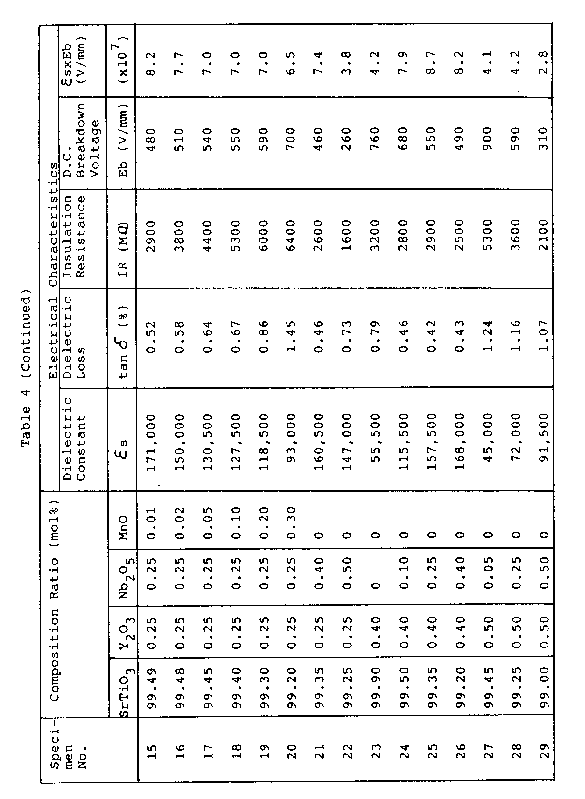


- As can be seen from Table 4 and 5, the semiconductive ceramic composition of the present invention was increased in dielectric constant (εs) to a level as high as about 115000 or more and highly decreased in dielectric loss (tan δ) to 0.35 to 0.86%.
- Also, Tables 4 and 5 indicates that addition of only one of Y₂O₃ or Nb₂O₅ as the additive for semiconductivity causes the composition to fail to be increased in dielectric constant (εs) and D.C breakdown voltage (Eb) (Specimen Nos. 1, 2, 3, 7, 11 and 23). Also, addition of both Y₂O₃ and Nb₂O₅ each in an amount below 0.1 mol% failed in a significant increase in dielectric constant and D.C breakdown voltage (Specimen Nos. 4, 5, 6, 12 and 27). Further, Y₂O₃ exceeding 0.4 mol% decreased the dielectric constant (Specimen Nos. 27 to 29) and Nb₂O₅ exceeding 0.4 mol% decreased D.C breakdown voltage (Specimen Nos. 6, 22 and 29).
- Furthermore, MnO below 0.02 mol% failed in a significant increase in insulation resistance IR (Specimen Nos. 14 and 15), wherein MnO exceeding 0.2 mol% caused an increase in dielectric loss and a decrease in dielectric constant (Specimen No. 20).
- In addition, Table 5 indicates that SiO₂ in an amount below 0.01 mol% causes an appropriate range of a SrO/TiO₂ ratio to be narrowed to 0.002 (Specimen Nos. 30-37), whereas SiO₂ above 0,10 mol% leaded to a decrease in dielectric constant (Specimen Nos. 50 and 51). On the contrary, SiO₂ in an amount of 0.01 to 0.1 mol% enlarged an appropriate range of a SrO/TiO₂ to 0.004 to 0.006.
- A semiconductive ceramic capacitor provided with zinc and copper electrodes was prepared using the so-prepared semiconductive ceramic body according to the following procedures.
- Preparation of Zinc Paste:
100 parts by weight zinc powder having an average particle diameter of 2.5 µm was used, and B₂O₃ (25 wt%)-SiO₂ (10 wt%)-ZnO (65 wt%) system frit glass powder having a particle size passing through a sieve of 325 mesh was added to the zinc powder at a mixing ratio shown in Table 6. Further, fine silver or metal oxide powder and an organic vehicle of ethyl cellulose and butyl carbitol acting as an organic binder were added thereto to form a mixture, which was then mixed while stirring to prepare a zinc paste.

- Formation of first conductive layer:
First conductive layers were formed on surfaces of the semiconductive ceramic body using the zinc paste prepared as described above. A 200 mesh screen formed of polyester synthetic resin sold under a tradename "Tetoron" was used to apply the zinc paste onto an upper surface of the semiconductive ceramic body by printing. Then, the ceramic body was dried at 125°C for about 10 minutes in a drying oven. - The zinc paste was also applied onto a lower surface of the semiconductive ceramic body and dried in substantially the same manner as described above and then supplied to a batch furnace while being carried on a stainless steel wire mesh to be burned at about 700°C for 10 minutes. A time used for the burning was about 60 minutes in all including temperature rise and fall operation. Thus, a first conductive layer mainly consisting of zinc and having a diameter of about 7.5mm was formed on each of both surfaces of the semiconductive ceramic body. Thus obtained ceramic body had such a structure as shown in Fig. 1.
- Preparation of copper paste
100 parts by weight copper powder having an average particle diameter of 0.5µm was used, and B₂O₃ (50 wt%)PbO(50 wt%) system frit glass powder having a particle size passing through a sieve of 325 mesh was added to the copper powder at a mixing ratio shown in Table 5, and further metal oxide powder and an organic vehicle consisting of ethyl cellulose and butyl carbitol and acting as an organic binder were added thereto and mixed together while stirring to prepare a copper paste. - Formation of Second Conductive Layer:
The so-prepared copper paste was applied onto each of the first conductive layers by printing and dried in substantially the same manner as in the zinc paste described above. Then, it was burned at 360°C for 20 minutes in a stream of a reducing atmosphere (90%N₂ + 10%H₂) to carry out baking, resulting in a second conductive layer which mainly consists of copper and has a diameter of about 5mm being formed on each of the first conductive layers in substantially the same manner as shown in Fig. 2. Thus, a semiconductive ceramic capacitor of the present invention was prepared which comprises the semiconductive ceramic body, the first conductive layers deposited on both surfaces of the body and mainly consisting of zinc, the second conductive layers deposited on the first conductive layers and mainly consisting of copper and had substantially the structure as shown in Fig. 3. - Evaluation of Electrode:
In order to evaluate the electrodes of the so-obtained semiconductive ceramic capacitor, dielectric constant (εs), dielectric loss tangent (tan δ), solderability and tensile strength of the electrodes were measured. The results were as shown in Table 6. - In order to determine criteria of judgement of the electrodes of the semiconductive ceramic capacitor of the present invention, a conventional SrTiO₃ system semiconductive ceramic capacitor having a silver electrode structure (hereinafter referred to as "conventional capacitor") was manufactured according to the following procedures. More particularly, a SrTiO₃ system semiconductive ceramic body having substantially the same composition and shape as that of this example was prepared and a silver paste was deposited on one surface of the ceramic body by baking according to a conventional method to form a silver electrode thereon. Then, electrical and mechanical tests were carried out on the conventional capacitor to measure its dielectric constant (εs), dielectric loss tangent (tan δ) (%), solderability and tensile strength T (kg) of the electrode. The results indicated that dielectric constant (εs) is 75,000, dielectric loss tangent (tanδ) is 0.5%, solderability is good and tensile strength T is 1.4kg. In view of the test results on the conventional capacitor, it was supposed that a semiconductive ceramic capacitor is successful of which dielectric constant is 100,000 or more, dielectric loss tangent is 1.0% or less, solderability is the same level as the conventional capacity or more, and tensile strength T is 0.5kg or more.
- Also, for comparison, tests were carried out on the conventional capacitor which has such a structure as shown in Fig. 1 or includes first conductive layers but lacks second conductive layers. The results were that the dielectric constant and dielectric loss tangent were as those of the ceramic capacitor of this example, however, soldering was completely failed and measuring of tensile strength was not possible.
- As is apparent from Table 6, the ceramic capacitor indicated by Specimen Nos. 4 to 26 is non-defective and is significantly increased in dielectric constant and tensile strength as compared with the conventional capacitor. Thus, it will be noted that the example allows a ceramic capacitor to be small-sized.
- Also, costs of zinc powder and copper powder used in the example are about 1/200 and 1/50 that of silver powder used in the conventional capacitor, respectively, resulting in the manufacturing cost being substantially decreased. Formation of the first and second conductive layers is carried out by screen printing or the like, accordingly, there is no fear that the ceramic body is exposed to damage such as corrosion by a plating solution sufficient to cause deterioration of reliability of the capacitor.
- Thus, it will be noted that the semiconductive ceramic composition and capacitor of the example effectively exhibit the above-noted advantages of the present invention.
- Also, the example revealed the following.
- (a) The above-noted advantages of the example were exhibited when zinc powder having an average particle diameter of each of 5µm, 10µm and 30µm was used.
- (b) The above-noted advantages of the example were also exhibited when when copper powder having an average particle diameter of each of 0.1µm, 0.3µm, 1µm, 5µm and 10µm was used.
- (c) Use of various glass powders each having a softening point ranging from 330°C to 800°C as the glass powder for each of the zinc paste and copper paste caused the above-noted advantage of the example to be exhibited. More particularly, use of conventional frit glasses each consisting of at least two selected from the group consisting of PbO, ZnO, Bi₂O₃ BaO, B₂O₃, SiO₂, ZrO₂, TiO₂ Al₂O₃ CaO and SrO and each having a softening point ranging from 330°C to 800°C exhibited the same results. Such frit glasses include a PbO-B₂O₃ system, PbO-B₂O₃-SiO₂ system, ZnO-B₂O₃-BiO₂ system and the like.
- (d) It was found that a temperature for baking the zinc paste for formation of the first conductive layer is preferably between a melting point of zinc (419.5°C) and a boiling point thereof (930°C), and more preferably between 500°C and 900°C. A temperature below the melting point resulted in a failure in formation of a practical first conductive layer and a decrease in tensile strength of the layer, whereas that above the boiling point promotes oxidation of zinc sufficient to lead to an increase in electrical resistance.
- (e) It was also found that a temperature for baking the copper paste for formation of the second conductive layer is preferably between 200°C and 800°C, and more preferably between 250°C and 500°C. A temperature below 200°C failed in sufficient bonding between the first conductive layer and the second conductive layer to decrease tensile strength of the electrode. A temperature above 800°C caused reduction of the surface of the semiconductive ceramic body to deteriorate characteristics of the capacitor.
- A semiconductive ceramic composition and a semiconductive ceramic capacitor which includes electrodes formed of aluminum and copper were prepared.
- Example 1 was substantially repeated to obtain each composition which has a composition ratio as shown in Table 7 and 8.


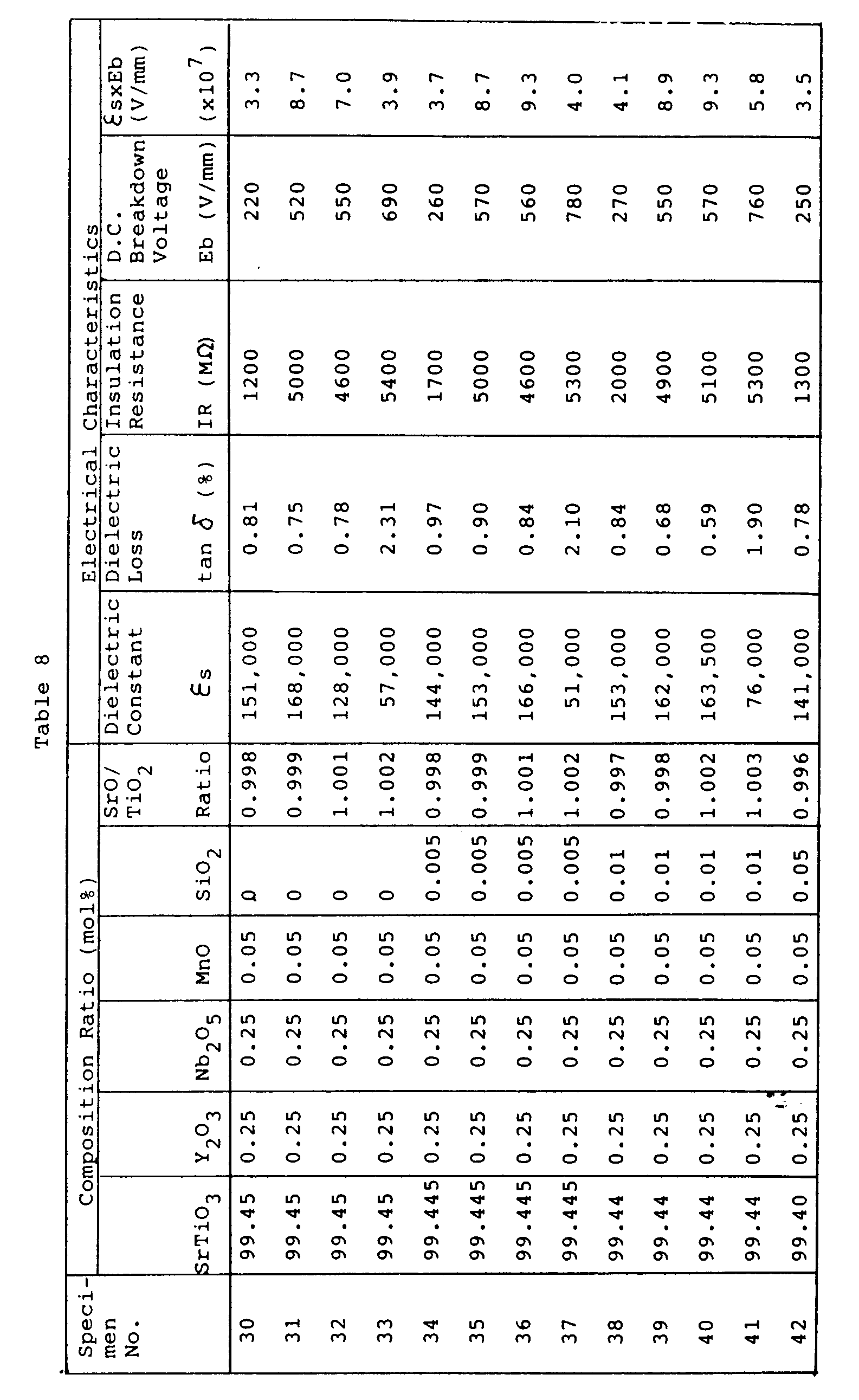

- The so-prepared each specimen had electrical characteristics as shown in Tables 7 and 8, wherein dielectric constant (εs) and dielectric loss (tan δ) were measured at a frequency of 1kHz and insulation resistance was measured at a room temperature of 20°C under the application of 50V.
- As can be seen from Table 7 and 8, the semiconductive ceramic composition of the present invention was increased in dielectric constant (εs) to a level as high as about 110000 or more and highly decreased in dielectric loss (tan δ) to 0.38 to 0.92%.
- Also, Tables 7 and 8 indicate that addition of only one of Y₂O₃ or Nb₂O₅ as the additive for semiconductivity causes the composition to fail to be increased in dielectric constant (εs) and D.C breakdown voltage (Eb) (Specimen Nos. 1, 2, 3, 7, 11 and 23). Also, addition of both Y₂O₃ and Nb₂O₅ each in an amount below 0.1 mol% failed in a significant increase in dielectric constant and D.C breakdown voltage (Specimen Nos. 4, 5, 6, 12 and 27). Further, Y₂O₃ exceeding 0.4 mol% decreased the dielectric constant (Specimen Nos. 27 to 29) and Nb₂O₅ exceeding 0.4 mol% decreased D.C breakdown voltage (Specimen Nos. 6, 22 and 29).
- Furthermore, MnO below 0.02 mol% failed in a significant increase in insulation resistance IR (Specimen Nos. 14 and 15), wherein MnO exceeding 0.2 mol% caused an increase in dielectric loss and a decrease in dielectric constant (Specimen No. 20).
- In addition, Table 8 indicates that SiO₂ in an amount below 0.01 mol% causes an appropriate range of a SrO/TiO₂ ratio to be narrowed to 0.002 (Specimen Nos. 30-37), whereas SiO₂ above 0,10 mol% leaded to a decrease in dielectric constant (Specimen Nos. 50 and 51). On the contrary, SiO₂ in an amount of 0.01 to 0.1 mol% enlarged an appropriate range of a SrO/TiO₂ to 0.004 to 0.006.
- A semiconductive ceramic capacitor provided with aluminum and copper electrodes was prepared using the so-prepared semiconductive ceramic body according to the following procedures.
- Preparation of aluminum paste:
100 parts by weight aluminum powder having an average particle diameter of 10µm was used, and B₂O₃ (25 wt%)-SiO₂ (10 wt%)-ZnO (65 wt%) system frit glass powder having a particle size passing through a sieve of 325 mesh was added to the aluminum powder at a mixing ratio shown in Table 9. Further, fine silver or metal oxide powder and an organic vehicle of ethyl cellulose and butyl carbitol acting as an organic binder were added thereto to form a mixture, which was then mixed while stirring to prepare an aluminum paste.

- Formation of first conductive layer:
First conductive layers were formed on surfaces of the semiconductive ceramic body using the aluminum paste prepared as described above. A 200 mesh screen formed of polyester synthetic resin sold under a tradename "Tetoron" was used to apply the aluminum paste onto an upper surface of the semiconductive ceramic body by printing. Then, the ceramic body was dried at 125°C for about 10 minutes in a drying oven. - The aluminum paste was also applied onto a lower surface of the semiconductive ceramic body and dried in substantially the same manner as described above and then supplied to a batch furnace while being carried on a stainless steel wire mesh to be burned at about 900°C for 10 minutes. A time used for the burning was about 60 minutes in all including temperature rise and fall operation. Thus, a first conductive layer mainly consisting of aluminum and having a diameter of about 7.5mm was formed on each of both surfaces of the semiconductive ceramic body.
- Preparation of copper paste:
100 parts by weight copper powder having an average particle diameter of 0.5µm was used, and B₂O₃ (50 wt%)PbO(50 wt%) system frit glass powder having a particle size passing through a sieve of 325 mesh was added to the copper powder at mixing ratios shown in Table 9, and further metal oxide powder and an organic vehicle consisting of ethyl cellulose and butyl carbitol and acting as an organic binder were added thereto and mixed together while stirring to prepare a copper paste. - Formation of second conductive layer:
The so-prepared copper paste was applied onto each of the first conductive layers by printing and dried in substantially the same manner as in the aluminum paste described above. Then, it was burned at 360°C for 20 minutes in a stream of a reducing atmosphere (90%N₂ + 10%H₂) to carry out baking, resulting in a second conductive layer which mainly consists of copper and has a diameter of about 5mm being formed on each of the first conductive layers. Thus, a semiconductive ceramic capacitor of the present invention was prepared which comprises the semiconductive ceramic body, the first conductive layers deposited on both surfaces of the body and mainly consisting of aluminum, the second conductive layers deposited on the first conductive layers and mainly consisting of copper. - Evaluation of Electrode:
Evaluation of the electrodes of the so-obtained semiconductive ceramic capacitor was carried out in substantially the same manner as in Example 2. The results were as shown in Table 9. - As is apparent from Table 9, the ceramic capacitor indicated by Specimen Nos. 4 to 26 is non-defective and is significantly increased in dielectric constant and tensile strength as compared with the conventional capacitor. Thus, it will be noted that the example allows a ceramic capacitor to be small-sized.
- Also, costs of aluminum powder and copper powder used in the example are about 1/100 and 1/50 that of silver powder used in the conventional capacitor, respectively, resulting in the manufacturing cost being substantially decreased. Formation of the first and second conductive layers is carried out by screen printing or the like, accordingly, there is no fear that the ceramic body is exposed to damage such as corrosion by a plating solution sufficient to cause deterioration of reliability of the capacitor.
- Thus, it will be noted that the semiconductive ceramic composition and capacitor of this example likewise exhibit the above-noted advantages of the present invention.
- Also, the example reveals the following as well as substantially the same facts indicated in items (a) to (c) and (e) of Example 2.
- More particularly, it was found that a temperature for baking the aluminum paste for formation of the first conductive layer is preferably between a melting point of Aluminum (660.2°C) and a boiling point thereof (about 2060°C), and more preferably between 800°C and 1200°C. A temperature below the melting point resulted in a failure in formation of a practical first conductive layer and a decrease in tensile strength of the layer, whereas that above the boiling point promotes oxidation of Aluminum sufficient to lead to an increase in electrical resistance.
- While the invention has been described with a certain degree of particularity with reference to the examples, obvious modifications and variations are possible in the light of the above teachings. It is therefore to be understood that within the scope of the appended claims, the invention may be practiced otherwise than as specifically described.
Claims (18)
- A semiconductive ceramic composition comprising:
a base material comprising SrTiO₃;
an additive for semiconductivity comprising Y₂O₃ and Nb₂O₅, said Y₂O₃ and Nb₂O₅ each being present in an amount of 0.1 to 0.4 mol% based on said composition, characterized in that the composition further comprises SiO₂ which is present in an amount of 0.01 to 0.1 mol%. - A semiconductive ceramic composition as defined in Claim 1 further comprising MnO which is present in an amount of 0.02 to 0.2 mol% based on said composition.
- A semiconductive ceramic composition as defined in Claim 1 wherein said composition is subjected to sintering after application of a Bi containing agent to cause Bi to be present at a grain boundary of said composition.
- A semiconductive ceramic capacitor comprising:
a semiconductive ceramic body formed of a
semiconductive ceramic composition as claimed in one of the preceding claims;
a first conductive layer deposited on a surface of said semiconductive ceramic body, said first conductive layer being formed of a material mainly consisting of metal powder selected from the group consisting of zinc powder and aluminum powder; and
a second conductive layer deposited on said first conductive layer, said second conductive layer being formed of a material mainly consisting of copper powder. - A semiconductive ceramic capacitor as defined in Claim 4, wherein said first and second conductive layers are formed by baking.
- A semiconductive ceramic capacitor as defined in Claim 4, wherein said material for said first conductive layer mainly consists of zinc and further contains at least one metal of Ag, Al and Cu.
- A semiconductive ceramic capacitor as defined in Claim 6, wherein said at least one metal contained in said first conductive layer is added in the form of its simple substance.
- A semiconductive ceramic capacitor as defined in Claim 6, wherein said at least one metal contained in said first conductive layer is added in the form of its oxide.
- A semiconductive ceramic capacitor as defined in Claim 6, wherein said second conductive layer further contains metal oxide.
- A process for manufacturing a semiconductive ceramic capacitor as claimed in one of the claims 4 to 9 comprising the steps of:
applying a first conductive paste onto a surface of a semiconductive ceramic body and baking said first conductive paste to form a first conductive layer on said semiconductive ceramic body, said first conductive paste mainly consisting of metal powder selected from the group consisting of zinc powder and aluminum powder; and
applying a second conductive paste onto a surface of said first conductive layer and baking said second conductive paste to form a second conductive layer on said first conductive layer, said second conductive paste mainly consisting of copper powder. - A process as defined in Claim 10, wherein baking of said second conductive paste is carried out in a neutral or reducing atmosphere.
- A process as defined in Claim 10, wherein said first conductive paste contains zinc powder, glass powder, and powder of at least one material selected from the group consisting of silver, aluminum, copper and their oxides.
- A process as defined in Claim 12, wherein said first conductive paste further contains an organic vehicle.
- A process as defined in Claim 10, wherein said first conductive paste contains aluminum powder, glass powder, and powder of at least one material selected from the group consisting of silver, zinc, copper and their oxides.
- A process as defined in Claim 14, wherein said first conductive paste further contains an organic vehicle.
- A process as defined in Claim 10, wherein said second conductive paste contains copper powder, glass powder and an organic vehicle.
- A process as defined in Claim 10, wherein said second conductive paste contains copper powder, glass powder and metal oxide powder.
- A process as defined in Claim 17, wherein said second conductive paste further contains an organic vehicle.
Applications Claiming Priority (4)
| Application Number | Priority Date | Filing Date | Title |
|---|---|---|---|
| JP176632/86 | 1986-07-29 | ||
| JP17663286A JPH0734412B2 (en) | 1986-07-29 | 1986-07-29 | Semiconductor ceramic capacitor and manufacturing method thereof |
| JP17663386A JPH0734413B2 (en) | 1986-07-29 | 1986-07-29 | Semiconductor ceramic capacitor and manufacturing method thereof |
| JP176633/86 | 1986-07-29 |
Publications (3)
| Publication Number | Publication Date |
|---|---|
| EP0255072A2 EP0255072A2 (en) | 1988-02-03 |
| EP0255072A3 EP0255072A3 (en) | 1989-05-10 |
| EP0255072B1 true EP0255072B1 (en) | 1993-04-21 |
Family
ID=26497478
Family Applications (1)
| Application Number | Title | Priority Date | Filing Date |
|---|---|---|---|
| EP87110807A Expired - Lifetime EP0255072B1 (en) | 1986-07-29 | 1987-07-25 | Semiconductive ceramic composition and semiconductive ceramic capacitor |
Country Status (5)
| Country | Link |
|---|---|
| US (2) | US4799127A (en) |
| EP (1) | EP0255072B1 (en) |
| KR (1) | KR920003225B1 (en) |
| CN (1) | CN1011838B (en) |
| DE (1) | DE3785506T2 (en) |
Families Citing this family (24)
| Publication number | Priority date | Publication date | Assignee | Title |
|---|---|---|---|---|
| EP0255072B1 (en) * | 1986-07-29 | 1993-04-21 | TDK Corporation | Semiconductive ceramic composition and semiconductive ceramic capacitor |
| JPH0616459B2 (en) * | 1987-07-23 | 1994-03-02 | 株式会社村田製作所 | Method for manufacturing porcelain capacitor |
| EP0337373A3 (en) * | 1988-04-12 | 1991-02-13 | Matsushita Electric Industrial Co., Ltd. | Multi-layered dielectric element |
| US4870539A (en) * | 1989-01-17 | 1989-09-26 | International Business Machines Corporation | Doped titanate glass-ceramic for grain boundary barrier layer capacitors |
| EP0412167B1 (en) * | 1989-02-16 | 1995-12-20 | Matsushita Electric Industrial Co., Ltd. | Laminated type grain boundary insulated semiconductor ceramic capacitor and method of producing the same |
| DE69023316T2 (en) * | 1989-03-22 | 1996-07-04 | Matsushita Electric Ind Co Ltd | CERAMIC CAPACITOR OF A SEMICONDUCTOR TYPE WITH LAMINATED AND CORN-INSULATED BORDER LAYERS. |
| EP0418394B1 (en) * | 1989-04-04 | 1995-08-23 | Matsushita Electric Industrial Co., Ltd. | Process for producing ceramic capacitors having varistor characteristics |
| US5061686A (en) * | 1989-05-15 | 1991-10-29 | Hewlett-Packard Company | Superconducting power distribution structure for integrated circuits |
| CA2033582A1 (en) | 1990-01-11 | 1991-07-12 | Galeb H. Maher | Fine grained batio3 powder mixture and method for making |
| US5010443A (en) * | 1990-01-11 | 1991-04-23 | Mra Laboratories, Inc. | Capacitor with fine grained BaTiO3 body and method for making |
| JP2757587B2 (en) * | 1990-06-26 | 1998-05-25 | 松下電器産業株式会社 | Grain boundary insulating semiconductor ceramic capacitor and method of manufacturing the same |
| JP2885616B2 (en) * | 1992-07-31 | 1999-04-26 | 株式会社東芝 | Semiconductor device and manufacturing method thereof |
| US5378667A (en) * | 1993-12-10 | 1995-01-03 | Korea Institute Of Science And Technology | Intercrystalline semiconductive ceramic capacitor |
| CN1056130C (en) * | 1994-05-06 | 2000-09-06 | 清华大学 | Method for making strontium titanate base grain-boundary layer capacitor material |
| CN1056939C (en) * | 1995-06-08 | 2000-09-27 | 西安九元高压电容器厂 | A.C. safety ceramic capacitor and making method thereof |
| US6442813B1 (en) * | 1996-07-25 | 2002-09-03 | Murata Manufacturing Co., Ltd. | Method of producing a monolithic ceramic capacitor |
| CN1049644C (en) * | 1997-03-21 | 2000-02-23 | 中国科学院上海硅酸盐研究所 | Process of preparing strontium-barium titanate film by using water as solvent for precursor solution |
| US6171988B1 (en) | 1999-07-30 | 2001-01-09 | International Business Machines Corporation | Low loss glass ceramic composition with modifiable dielectric constant |
| US20020092583A1 (en) * | 2001-01-16 | 2002-07-18 | Pelton Alan R. | Medical devices, particularly stents, and methods for their manufacture |
| TW556237B (en) * | 2001-09-14 | 2003-10-01 | Matsushita Electric Industrial Co Ltd | Ceramic capacitor |
| US6838828B2 (en) * | 2001-11-05 | 2005-01-04 | Lg Electronics Inc. | Plasma display panel and manufacturing method thereof |
| US7378793B2 (en) * | 2001-11-13 | 2008-05-27 | Lg Electronics Inc. | Plasma display panel having multiple shielding layers |
| US8866018B2 (en) | 2009-01-12 | 2014-10-21 | Oak-Mitsui Technologies Llc | Passive electrical devices and methods of fabricating passive electrical devices |
| CN109928753A (en) * | 2019-03-14 | 2019-06-25 | 杭州电子科技大学 | A kind of low-k silicon substrate microwave dielectric ceramic materials and preparation method thereof |
Family Cites Families (20)
| Publication number | Priority date | Publication date | Assignee | Title |
|---|---|---|---|---|
| US3637435A (en) * | 1969-07-08 | 1972-01-25 | Gen Motors Corp | Metallizing process for glass-free ceramics bodies |
| US3933668A (en) * | 1973-07-16 | 1976-01-20 | Sony Corporation | Intergranular insulation type polycrystalline ceramic semiconductive composition |
| DE2839976A1 (en) * | 1977-09-16 | 1979-03-29 | Murata Manufacturing Co | Semiconductor ceramics for boundary layer capacitors |
| US4403236A (en) * | 1979-10-09 | 1983-09-06 | Murata Manufacturing Co., Ltd. | Boundary layer type semiconducting ceramic capacitors with high capacitance |
| JPS5674913A (en) * | 1979-11-26 | 1981-06-20 | Tdk Electronics Co Ltd | Semiconductor porcelain composition |
| JPS56110219A (en) * | 1980-02-04 | 1981-09-01 | Taiyo Yuden Kk | Porcelain capacitor |
| JPS56162820A (en) * | 1980-05-20 | 1981-12-15 | Kiyoshi Okazaki | Vapor bank layered laminated ceramic capacitor and method of manufacturing same |
| JPS578175A (en) * | 1980-06-19 | 1982-01-16 | Nec Corp | Multilayer interconnection structure for crossover and manufacture thereof |
| US4380559A (en) * | 1980-09-25 | 1983-04-19 | Murata Manufacturing Co., Ltd. | Method for producing boundary layer semiconductor ceramic capacitors |
| JPS57143203A (en) * | 1981-02-27 | 1982-09-04 | Taiyo Yuden Kk | Conductive paste for forming conductive layer by baking on porcelain |
| JPS57160960A (en) * | 1981-03-30 | 1982-10-04 | Murata Manufacturing Co | Intergranular insulation semiconductor ceramic composition |
| JPS57180112A (en) * | 1981-04-30 | 1982-11-06 | Taiyo Yuden Kk | Method of forming electrode for porcelain electronic part |
| GB2102026B (en) * | 1981-06-05 | 1985-07-10 | Matsushita Electric Industrial Co Ltd | Conductive pastes |
| JPS5891602A (en) * | 1981-11-26 | 1983-05-31 | 太陽誘電株式会社 | Voltage nonlinear porcelain composition |
| US4511601A (en) * | 1983-05-13 | 1985-04-16 | North American Philips Corporation | Copper metallization for dielectric materials |
| EP0153412B1 (en) * | 1983-06-28 | 1989-03-22 | Matsushita Electric Industrial Co., Ltd. | Voltage-dependent, non-linear resistor porcelain composition |
| JPS607703A (en) * | 1983-06-28 | 1985-01-16 | 松下電器産業株式会社 | Voltage depending nonlinear resistor porcelain composition |
| US4604676A (en) * | 1984-10-02 | 1986-08-05 | Murata Manufacturing Co., Ltd. | Ceramic capacitor |
| EP0255072B1 (en) * | 1986-07-29 | 1993-04-21 | TDK Corporation | Semiconductive ceramic composition and semiconductive ceramic capacitor |
| US4807085A (en) * | 1987-05-28 | 1989-02-21 | Iwasaki Electric Co., Ltd. | Nonlinear capacitor for generating high-voltage pulses |
-
1987
- 1987-07-25 EP EP87110807A patent/EP0255072B1/en not_active Expired - Lifetime
- 1987-07-25 DE DE8787110807T patent/DE3785506T2/en not_active Expired - Fee Related
- 1987-07-28 CN CN87105776A patent/CN1011838B/en not_active Expired
- 1987-07-29 US US07/079,018 patent/US4799127A/en not_active Expired - Lifetime
- 1987-07-29 KR KR1019870008286A patent/KR920003225B1/en not_active Expired
-
1988
- 1988-11-15 US US07/272,139 patent/US4854936A/en not_active Expired - Lifetime
Also Published As
| Publication number | Publication date |
|---|---|
| DE3785506D1 (en) | 1993-05-27 |
| EP0255072A3 (en) | 1989-05-10 |
| EP0255072A2 (en) | 1988-02-03 |
| US4799127A (en) | 1989-01-17 |
| CN1011838B (en) | 1991-02-27 |
| DE3785506T2 (en) | 1993-08-12 |
| US4854936A (en) | 1989-08-08 |
| KR920003225B1 (en) | 1992-04-24 |
| KR880001549A (en) | 1988-04-25 |
| CN87105776A (en) | 1988-02-24 |
Similar Documents
| Publication | Publication Date | Title |
|---|---|---|
| US4854936A (en) | Semiconductive ceramic composition and semiconductive ceramic capacitor | |
| EP0071930B1 (en) | Thick film conductor compositions | |
| US4416932A (en) | Thick film conductor compositions | |
| US4528613A (en) | Ceramic glass material, capacitor made therefrom and method of making the same | |
| EP0059852B1 (en) | An electroconductive paste to be baked on ceramic bodies to provide capacitors, varistors or the like | |
| CA1206779A (en) | Thick film conductor compositions | |
| JP3851295B2 (en) | Low temperature fired dielectric composition, multilayer ceramic capacitor and ceramic electronic component | |
| EP0517213A2 (en) | Ceramic capacitor and method for fabricating the same | |
| JP2003077336A (en) | Conductive paste and multilayer ceramic capacitor using the same | |
| US5091820A (en) | Ceramic piezoelectric element with electrodes formed by reduction | |
| DE10015689C2 (en) | Dielectric ceramic composition, electrical component and method for its production | |
| JPS6310887B2 (en) | ||
| EP0290859A2 (en) | Low temperature sintered ceramic capacitor having a high resistivity and bending strength, and method of manufacture | |
| EP0788123A2 (en) | Dielectric ceramic composition | |
| JPS6127003A (en) | Conductive paste composition | |
| KR920009172B1 (en) | Semiconductive ceramic composition and semiconductive ceramic capacitor | |
| JPS593909A (en) | Electrode paste for ceramic condenser | |
| JPH1012043A (en) | Conductive composition and boundary layer ceramic capacitor | |
| JPH0231446B2 (en) | ATSUMAKUDOTAISOSEIBUTSU | |
| EP0044076A1 (en) | Screen-printable dielectric composition | |
| JP3070238B2 (en) | Manufacturing method of multilayer ceramic element | |
| JPH0734413B2 (en) | Semiconductor ceramic capacitor and manufacturing method thereof | |
| DE3926505C2 (en) | Non-reductive agent for dielectric ceramic material | |
| JPH0734414B2 (en) | Semiconductor ceramic capacitor and manufacturing method thereof | |
| JPH0734412B2 (en) | Semiconductor ceramic capacitor and manufacturing method thereof |
Legal Events
| Date | Code | Title | Description |
|---|---|---|---|
| PUAI | Public reference made under article 153(3) epc to a published international application that has entered the european phase |
Free format text: ORIGINAL CODE: 0009012 |
|
| AK | Designated contracting states |
Kind code of ref document: A2 Designated state(s): DE FR GB NL |
|
| PUAL | Search report despatched |
Free format text: ORIGINAL CODE: 0009013 |
|
| AK | Designated contracting states |
Kind code of ref document: A3 Designated state(s): DE FR GB NL |
|
| 17P | Request for examination filed |
Effective date: 19891026 |
|
| 17Q | First examination report despatched |
Effective date: 19910221 |
|
| GRAA | (expected) grant |
Free format text: ORIGINAL CODE: 0009210 |
|
| AK | Designated contracting states |
Kind code of ref document: B1 Designated state(s): DE FR GB NL |
|
| ET | Fr: translation filed | ||
| REF | Corresponds to: |
Ref document number: 3785506 Country of ref document: DE Date of ref document: 19930527 |
|
| PLBE | No opposition filed within time limit |
Free format text: ORIGINAL CODE: 0009261 |
|
| STAA | Information on the status of an ep patent application or granted ep patent |
Free format text: STATUS: NO OPPOSITION FILED WITHIN TIME LIMIT |
|
| 26N | No opposition filed | ||
| PGFP | Annual fee paid to national office [announced via postgrant information from national office to epo] |
Ref country code: FR Payment date: 19980709 Year of fee payment: 12 |
|
| PGFP | Annual fee paid to national office [announced via postgrant information from national office to epo] |
Ref country code: GB Payment date: 19980716 Year of fee payment: 12 |
|
| PGFP | Annual fee paid to national office [announced via postgrant information from national office to epo] |
Ref country code: NL Payment date: 19980728 Year of fee payment: 12 |
|
| PGFP | Annual fee paid to national office [announced via postgrant information from national office to epo] |
Ref country code: DE Payment date: 19980803 Year of fee payment: 12 |
|
| PG25 | Lapsed in a contracting state [announced via postgrant information from national office to epo] |
Ref country code: GB Free format text: LAPSE BECAUSE OF NON-PAYMENT OF DUE FEES Effective date: 19990725 |
|
| PG25 | Lapsed in a contracting state [announced via postgrant information from national office to epo] |
Ref country code: FR Free format text: THE PATENT HAS BEEN ANNULLED BY A DECISION OF A NATIONAL AUTHORITY Effective date: 19990731 |
|
| PG25 | Lapsed in a contracting state [announced via postgrant information from national office to epo] |
Ref country code: NL Free format text: LAPSE BECAUSE OF NON-PAYMENT OF DUE FEES Effective date: 20000201 |
|
| GBPC | Gb: european patent ceased through non-payment of renewal fee |
Effective date: 19990725 |
|
| NLV4 | Nl: lapsed or anulled due to non-payment of the annual fee |
Effective date: 20000201 |
|
| PG25 | Lapsed in a contracting state [announced via postgrant information from national office to epo] |
Ref country code: DE Free format text: LAPSE BECAUSE OF NON-PAYMENT OF DUE FEES Effective date: 20000503 |
|
| REG | Reference to a national code |
Ref country code: FR Ref legal event code: ST |