EP0253136A2 - Combined digital-to-analog converter and latch memory circuit - Google Patents
Combined digital-to-analog converter and latch memory circuit Download PDFInfo
- Publication number
- EP0253136A2 EP0253136A2 EP87108353A EP87108353A EP0253136A2 EP 0253136 A2 EP0253136 A2 EP 0253136A2 EP 87108353 A EP87108353 A EP 87108353A EP 87108353 A EP87108353 A EP 87108353A EP 0253136 A2 EP0253136 A2 EP 0253136A2
- Authority
- EP
- European Patent Office
- Prior art keywords
- current
- latch
- logic
- transistor
- subcircuits
- Prior art date
- Legal status (The legal status is an assumption and is not a legal conclusion. Google has not performed a legal analysis and makes no representation as to the accuracy of the status listed.)
- Ceased
Links
Images
Classifications
-
- H—ELECTRICITY
- H03—ELECTRONIC CIRCUITRY
- H03M—CODING; DECODING; CODE CONVERSION IN GENERAL
- H03M1/00—Analogue/digital conversion; Digital/analogue conversion
- H03M1/66—Digital/analogue converters
- H03M1/74—Simultaneous conversion
- H03M1/742—Simultaneous conversion using current sources as quantisation value generators
- H03M1/745—Simultaneous conversion using current sources as quantisation value generators with weighted currents
Definitions
- the present invention relates to digital-to-analog converters and, in particular, to a digital-to-analog converter circuit that combines a resistive ladder network of a conventional type with current-controlled latch memory subcircuits in a configuration that promotes the efficient use of space, power, and circuit elements.
- One type of conventional digital-to-analog converter uses an R-2R resistive ladder network in cooperation with a number of current sources that equals the number of bits of a binary word which is to be converted to an analog output voltage.
- the logic state of each bit of the binary word is stored in a separate latch circuit.
- Each of the latch circuits drives a separate current source which in response to the logic state of the bit delivers a current signal of a predetermined amount to a corresponding input node of the R-2R resistive ladder network.
- the analog output voltage is a weighted sum of the signals representing the bits in the binary word.
- a digital-to-analog converter circuit of this type suffers from the disadvantage requiring separate circuit elements to form the latch memory circuits and the constant- current sources.
- This type of circuit uses a number of circuit elements which occupy a relatively large amount of space, for example, on an integrated circuit substrate, and consume significant amounts of electrical power.
- An object of the present invention is, therefore, to provide a digital-to-analog converter that promotes the efficient use of space, power, and circuit elements.
- Another object of the invention is to provide such a digital-to-analog converter that combines the latch memory and current source in a single subcircuit for each bit in the digital word.
- a further object of the invention is to provide such a digital-to-analog converter that uses an R-2R resistive ladder network to synthesize the analog output signal.
- the present invention is a combined digital-to-analog converter and latch memory circuit.
- the circuit comprises a resistive ladder network that has plural input nodes and an analog output. Each of the input nodes corresponds to a different bit of a digital word that is to be converted to an analog signal.
- the circuit further comprises plural current-controlled latch subcircuits. Each of the latch subcircuits uses an amount of current to control the operation thereof and delivers the amount of current to one of the input nodes to represent the logic state of one of the bits of the digital word. The amount of current is, therefore, used to store the logic states of the bits of the digital word and to drive directly the resistive ladder network to synthesize an analog signal that corresponds to the weighted value of the digital word.
- the resistive ladder network is of the R-2R type and the current-controlled latch subcircuits are implemented in emitter function logic (EFL ) circuitry in the form of a serial loading shift register.
- EFL emitter function logic
- Each of the EFL elements of the shift register is of conventional design and includes a master section and a slave section with emitter follower transistors.
- the collectors of the emitter follower transistors in the master sections are connected directly to the input nodes of the R-2R resistive ladder network, and the collectors of the emitter follower transistors in the slave sections are connected directly to a collector bias supply voltage.
- the bits of the digital word are loaded serially into the shift register in response to an applied clock signal. Proper calibration of the amount of current delivered by the EFL circuitry promotes the operation of the shift register as a latch memory and as a current source that drives the R-2R resistive ladder network.
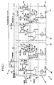
- Fig. 1 is an electrical circuit schematic diagram of the digital-to-analog converter circuit of the present invention.
- Fig. 1 is a diagram of a preferred embodiment of the combined digital-to-analog converter and latch memory circuit 10 of the present invention.
- Fig. 1 shows a section of an R-2R resistive ladder network 12 of conventional design and two subcircuits 14 and 16 of a current-controlled latch memory 18 that is implemented in circuitry of the EFL type.
- the number of subcircuits of latch memory 18 equals the number "N" of bits in the binary word to be converted to an analog signal.
- the subcircuits of latch memory 18 are connected to form a serial loading shift register.
- the bits of the digital word are applied in a serial stream to a data input 20 of subcircuit 14. These data bits shift progressively to the right to the next adjacent subcircuit in response to a differential voltage clock signal that is applied across a positive input terminal 22 and a negative input terminal 24.
- the data are loaded into latch memory 18 as the clock signal completes a transition from a logic 1 state to a logic 0 state.
- the digital word is completely loaded into latch memory 18 after N number of such transitions.
- subcircuits included in latch memory 18 are of the same conventional EFL circuit design and operate in the same manner. The following description is directed, therefore, only to the operation of subcircuit 16.
- Corresponding components of subcircuit 14 and of ladder network 12 are designated with identical reference numerals followed by primes. (Certain components in subcircuits 14 and 16 are undesignated because they need not be considered for the analysis presented below.)
- Subcircuit 16 is divided into a master section 40 and a slave section 42.
- Slave section 42 includes emitter coupled transistors 44 and 46 through which a constant current, "I" , flows from a constant-current source 48.
- the base terminal 50 of transistor 44 is connected to negative input terminal 24, and the base terminal 52 of transistor 46 is connected to positive input terminal 22.
- the current "I" flows from the collector 54 to the emitter 56 of transistor 44.
- the current flowing through collector 54 of transistor 44 flows through either emitter 58 of transistor 60 or the emitter 62 of transistor 64. This is determined by the magnitude of the voltage on the base 66 of transistor 60.
- the current "I” flows through transistor 60 and no current flows through transistor 64.
- the collector bias voltage, V CC equals 0 volts and the voltage V R equals - 0.3 volt.
- the current "I” flows through the collector 70 of transistor 60, which is connected to the resistor 72 of value 2"R" of ladder network 12. This indicates that a logic 1 is stored in subcircuit 16.
- the voltage on the base 74 of the transistor 76 is zero volts because the collector 78 of transistor 64 is connected to CC through the resistor 80, through which no current flows.
- the current "I” flows through transistor 64 and no current flows through transistor 60. This indicates that a logic 0 is stored in subcircuit 16. Under these conditions, the current "I” flows through collector 78 of transistor 64 and causes about - 0.6 volt to appear on base 74 of transistor 76.
- the clock signal is in a logic 1 state, i.e. , the voltage signal applied to positive input terminal 22 is of sufficient magnitude bias transistor 46 in the forward active region the current "I" flows from the collector 82 to the emitter 84 of transistor 46.
- the current flowing through collector 82 of transistor 46 flows through either the emitter 86 of transistor 64 or the emitter 88 of transistor 76. This is determined by the magnitude of the voltage on base 74 of transistor 76.
- transistor 76 If the voltage on base 74 of transistor 76 is less than ( i.e. , is about - 0.6 volt) the voltage on base 68 of transistor 64, the current "I" flows through collector 78 of transistor 64 and no current flows through transistor 76.
- each subcircuit 16 provides the current necessary to effect the latch memory function and to drive an input node of ladder network 12.
- the collector 70 of transistor 60 indicates that the bit stored in subcircuit 16 is a logic 1 and delivers a current "I" to the input node 102.
- the collector 70 ⁇ , of transistor 60 ⁇ indicates that the bit stored in subcircuit 14 is a logic 1 and delivers a current "I" to the input node 100.
- Input node 100 represents the most significant bit (MSB), and input node 102 represents the next most significant bit (MSB -1) of the digital word.
- Ladder network 12 synthesizes, therefore, an analog signal which appears on output terminal 104 of ladder network 12 and which represents the weighted value of the digital input word stored in latch memory 18.
- V LADDER - REF must be greater than V CC by an amount that is sufficient to prevent the saturation of the emitter follower transistors ( i.e. , transistors 60, 64, 76, and 94).
- the R-2R resistive ladder network is for converting digital words in binary format.
- the present invention can also be used with ladder networks of digital words in other number systems, such as binary coded decimal.
- the current "I" can be provided from the slave section of a latch memory subcircuit. In the case of subcircuit 18, the current "I" would be delivered to node 102 from collector 90 of transistor 76 and collector 70 of transistor 60 would be connected to V CC .
- the scope of the present invention should be determined, therefore, only by the following claims.
Abstract
Description
- The present invention relates to digital-to-analog converters and, in particular, to a digital-to-analog converter circuit that combines a resistive ladder network of a conventional type with current-controlled latch memory subcircuits in a configuration that promotes the efficient use of space, power, and circuit elements.
- One type of conventional digital-to-analog converter uses an R-2R resistive ladder network in cooperation with a number of current sources that equals the number of bits of a binary word which is to be converted to an analog output voltage. The logic state of each bit of the binary word is stored in a separate latch circuit. Each of the latch circuits drives a separate current source which in response to the logic state of the bit delivers a current signal of a predetermined amount to a corresponding input node of the R-2R resistive ladder network. The analog output voltage is a weighted sum of the signals representing the bits in the binary word.
- A digital-to-analog converter circuit of this type suffers from the disadvantage requiring separate circuit elements to form the latch memory circuits and the constant- current sources. This type of circuit uses a number of circuit elements which occupy a relatively large amount of space, for example, on an integrated circuit substrate, and consume significant amounts of electrical power.
- An object of the present invention is, therefore, to provide a digital-to-analog converter that promotes the efficient use of space, power, and circuit elements.
- Another object of the invention is to provide such a digital-to-analog converter that combines the latch memory and current source in a single subcircuit for each bit in the digital word.
- A further object of the invention is to provide such a digital-to-analog converter that uses an R-2R resistive ladder network to synthesize the analog output signal.
- The present invention is a combined digital-to-analog converter and latch memory circuit. The circuit comprises a resistive ladder network that has plural input nodes and an analog output. Each of the input nodes corresponds to a different bit of a digital word that is to be converted to an analog signal. The circuit further comprises plural current-controlled latch subcircuits. Each of the latch subcircuits uses an amount of current to control the operation thereof and delivers the amount of current to one of the input nodes to represent the logic state of one of the bits of the digital word. The amount of current is, therefore, used to store the logic states of the bits of the digital word and to drive directly the resistive ladder network to synthesize an analog signal that corresponds to the weighted value of the digital word.
- In a preferred embodiment, the resistive ladder network is of the R-2R type and the current-controlled latch subcircuits are implemented in emitter function logic (EFL ) circuitry in the form of a serial loading shift register. Each of the EFL elements of the shift register is of conventional design and includes a master section and a slave section with emitter follower transistors. The collectors of the emitter follower transistors in the master sections are connected directly to the input nodes of the R-2R resistive ladder network, and the collectors of the emitter follower transistors in the slave sections are connected directly to a collector bias supply voltage. The bits of the digital word are loaded serially into the shift register in response to an applied clock signal. Proper calibration of the amount of current delivered by the EFL circuitry promotes the operation of the shift register as a latch memory and as a current source that drives the R-2R resistive ladder network.
- Additional objects and advantages of the present invention will be apparent from the following detailed description of a preferred embodiment thereof, which proceeds with reference to the accompanying drawing.
- Fig. 1 is an electrical circuit schematic diagram of the digital-to-analog converter circuit of the present invention.
- Fig. 1 is a diagram of a preferred embodiment of the combined digital-to-analog converter and
latch memory circuit 10 of the present invention. Fig. 1 shows a section of an R-2Rresistive ladder network 12 of conventional design and twosubcircuits 14 and 16 of a current-controlledlatch memory 18 that is implemented in circuitry of the EFL type. The number of subcircuits oflatch memory 18 equals the number "N" of bits in the binary word to be converted to an analog signal. - The subcircuits of
latch memory 18 are connected to form a serial loading shift register. The bits of the digital word are applied in a serial stream to adata input 20 of subcircuit 14. These data bits shift progressively to the right to the next adjacent subcircuit in response to a differential voltage clock signal that is applied across apositive input terminal 22 and anegative input terminal 24. The data are loaded intolatch memory 18 as the clock signal completes a transition from alogic 1 state to a logic 0 state. The digital word is completely loaded intolatch memory 18 after N number of such transitions. - The subcircuits included in
latch memory 18 are of the same conventional EFL circuit design and operate in the same manner. The following description is directed, therefore, only to the operation ofsubcircuit 16. Corresponding components of subcircuit 14 and ofladder network 12 are designated with identical reference numerals followed by primes. (Certain components insubcircuits 14 and 16 are undesignated because they need not be considered for the analysis presented below.) -
Subcircuit 16 is divided into amaster section 40 and aslave section 42.Slave section 42 includes emitter coupledtransistors current source 48. Thebase terminal 50 oftransistor 44 is connected tonegative input terminal 24, and thebase terminal 52 oftransistor 46 is connected topositive input terminal 22. - Whenever the clock signal is in a logic 0 state, i.e, the voltage signal applied to
negative input terminal 24 is of sufficient magnitude to biastransistor 44 in the forward active region, the current "I" flows from the collector 54 to theemitter 56 oftransistor 44. The current flowing through collector 54 oftransistor 44 flows through eitheremitter 58 oftransistor 60 or theemitter 62 oftransistor 64. This is determined by the magnitude of the voltage on thebase 66 oftransistor 60. - If the voltage on
base 66 oftransistor 60 is greater than the reference voltage, VR, on the base 68 oftransistor 64, the current "I" flows throughtransistor 60 and no current flows throughtransistor 64. In a preferred embodiment, the collector bias voltage, VCC, equals 0 volts and the voltage VR equals - 0.3 volt. Under these conditions, the current "I" flows through thecollector 70 oftransistor 60, which is connected to theresistor 72 of value 2"R" ofladder network 12. This indicates that alogic 1 is stored insubcircuit 16. The voltage on thebase 74 of thetransistor 76 is zero volts because thecollector 78 oftransistor 64 is connected to CC through theresistor 80, through which no current flows. - If the voltage on
base 66 oftransistor 60 is less than (i.e, is about - 0.6 volt) the voltage VR on base 68 oftransistor 64, the current "I" flows throughtransistor 64 and no current flows throughtransistor 60. This indicates that a logic 0 is stored insubcircuit 16. Under these conditions, the current "I" flows throughcollector 78 oftransistor 64 and causes about - 0.6 volt to appear onbase 74 oftransistor 76. - The foregoing description assumes that the current "I" does not diminish as a function of the transistor α. parameters.
- In summary, whenever the clock signal is in the logic 0 state, the voltage on
base 66 oftransistor 60, which is located inmaster section 40, also appears onbase 74 oftransistor 76, which is inslave section 42. The transition of the clock signal from thelogic 1 state to the logic 0 state causes, therefore, a transfer of data frommaster section 40 toslave section 42. - Whenever the clock signal is in a
logic 1 state, i.e., the voltage signal applied topositive input terminal 22 is of sufficientmagnitude bias transistor 46 in the forward active region the current "I" flows from thecollector 82 to theemitter 84 oftransistor 46. The current flowing throughcollector 82 oftransistor 46 flows through either theemitter 86 oftransistor 64 or theemitter 88 oftransistor 76. This is determined by the magnitude of the voltage onbase 74 oftransistor 76. - If the voltage on
base 74 oftransistor 76 is greater than the voltage VR on base 68 oftransistor 64, the current "I" flows through thecollector 90 oftransistor 76 and no current flows throughtransistor 64. - If the voltage on
base 74 oftransistor 76 is less than (i.e., is about - 0.6 volt) the voltage on base 68 oftransistor 64, the current "I" flows throughcollector 78 oftransistor 64 and no current flows throughtransistor 76. - In summary, whenever the clock signal is in the
logic 1 state, the voltage onbase 74 oftransistor 76 does not change, i.e, there is no data transfer when the clock signal is in thelogic 1 state. The data remain, therefore, latched in thelatch memory 18. The data input and data output ofsubcircuit 16 are, respectively, theemitter 92 of thetransistor 94 and theemitter 96 oftransistor 76. It will be appreciated that each subcircuit provides the current necessary to effect the latch memory function and to drive an input node ofladder network 12. - Whenever it conducts current, the
collector 70 oftransistor 60 indicates that the bit stored insubcircuit 16 is alogic 1 and delivers a current "I" to theinput node 102. Similarly, whenever it conducts current, the collector 70ʹ, of transistor 60ʹ, indicates that the bit stored in subcircuit 14 is alogic 1 and delivers a current "I" to theinput node 100.Input node 100 represents the most significant bit (MSB), andinput node 102 represents the next most significant bit (MSB -1) of the digital word. - The contribution of the voltage that develops on an input node from the current "I" flowing through a subcircuit of
latch memory 18 equals one-half of that on the input node corresponding to the next most significant bit. For example, such voltages oninput nodes latch memory 18, an open circuit voltage appears on that input node. -
Ladder network 12 synthesizes, therefore, an analog signal which appears onoutput terminal 104 ofladder network 12 and which represents the weighted value of the digital input word stored inlatch memory 18. Typical values of the components used in the preferred embodiment are I = 0.5 mA, RL = 600 ohms, VR = - 0.3 volt, VEE = -5.2 volts, VCC = 0 volts, VLADDER - REF = + 1 volt, R = 1.5 kilohms, and 2R = 3 kilohms. VLADDER - REFmust be greater than VCC by an amount that is sufficient to prevent the saturation of the emitter follower transistors (i.e.,transistors - It will be obvious to those having skill in the art that many changes may be made to the details of the above-described preferred embodiment of the present invention without departing from the underlying principles thereof. For example, the R-2R resistive ladder network is for converting digital words in binary format. The present invention can also be used with ladder networks of digital words in other number systems, such as binary coded decimal. Moreover, the current "I" can be provided from the slave section of a latch memory subcircuit. In the case of
subcircuit 18, the current "I" would be delivered tonode 102 fromcollector 90 oftransistor 76 andcollector 70 oftransistor 60 would be connected to VCC. The scope of the present invention should be determined, therefore, only by the following claims.
Claims (3)
a resistive ladder network having plural input nodes and an output, each of the input nodes corresponding to a different bit of a digital word; and
plural current-controlled latch subcircuits, each of the latch subcircuits using an amount of current to control the operation thereof and delivering the amount of current to one of the input nodes to represent the logic state of a corresponding one of the bits, thereby to store in the latch subcircuits the logic states of the bits of the digital word and to provide at the output an analog signal that corresponds to the weighted value of the digital word.
Applications Claiming Priority (2)
| Application Number | Priority Date | Filing Date | Title |
|---|---|---|---|
| US888199 | 1986-07-18 | ||
| US06/888,199 US4733218A (en) | 1986-07-18 | 1986-07-18 | Combined digital-to-analog converter and latch memory circuit |
Publications (2)
| Publication Number | Publication Date |
|---|---|
| EP0253136A2 true EP0253136A2 (en) | 1988-01-20 |
| EP0253136A3 EP0253136A3 (en) | 1990-10-24 |
Family
ID=25392720
Family Applications (1)
| Application Number | Title | Priority Date | Filing Date |
|---|---|---|---|
| EP19870108353 Ceased EP0253136A3 (en) | 1986-07-18 | 1987-06-10 | Combined digital-to-analog converter and latch memory circuit |
Country Status (3)
| Country | Link |
|---|---|
| US (1) | US4733218A (en) |
| EP (1) | EP0253136A3 (en) |
| JP (1) | JPS6331226A (en) |
Families Citing this family (4)
| Publication number | Priority date | Publication date | Assignee | Title |
|---|---|---|---|---|
| US5172011A (en) * | 1989-06-30 | 1992-12-15 | Digital Equipment Corporation | Latch circuit and method with complementary clocking and level sensitive scan capability |
| US5148164A (en) * | 1990-04-23 | 1992-09-15 | Mitsubishi Denki Kabushiki Kaisha | Current generating device for complementarily generating two currents of different magnitudes in response to one-bit data |
| US5430336A (en) * | 1992-10-23 | 1995-07-04 | Sony Corporation | Emitter coupled logic circuit |
| US7158062B2 (en) * | 2004-01-21 | 2007-01-02 | Raytheon Company | Clocked DAC current switch |
Citations (2)
| Publication number | Priority date | Publication date | Assignee | Title |
|---|---|---|---|---|
| US4323795A (en) * | 1980-02-12 | 1982-04-06 | Analog Devices, Incorporated | Bias current network for IC digital-to-analog converters and the like |
| EP0115352A2 (en) * | 1983-01-31 | 1984-08-08 | Siemens Aktiengesellschaft | Integratable digital-analog converter |
Family Cites Families (1)
| Publication number | Priority date | Publication date | Assignee | Title |
|---|---|---|---|---|
| US4400690A (en) * | 1978-08-08 | 1983-08-23 | Analog Devices, Incorporated | A-to-D Converter of the successive-approximation type |
-
1986
- 1986-07-18 US US06/888,199 patent/US4733218A/en not_active Expired - Fee Related
-
1987
- 1987-06-10 EP EP19870108353 patent/EP0253136A3/en not_active Ceased
- 1987-06-30 JP JP62163843A patent/JPS6331226A/en active Granted
Patent Citations (2)
| Publication number | Priority date | Publication date | Assignee | Title |
|---|---|---|---|---|
| US4323795A (en) * | 1980-02-12 | 1982-04-06 | Analog Devices, Incorporated | Bias current network for IC digital-to-analog converters and the like |
| EP0115352A2 (en) * | 1983-01-31 | 1984-08-08 | Siemens Aktiengesellschaft | Integratable digital-analog converter |
Non-Patent Citations (1)
| Title |
|---|
| IEEE JOURNAL OF SOLID-STATE CIRCUITS, vol. SC-15, no. 6, December 1980, pages 1059-1070, IEEE, New York, US; B.E. AMAZEEN et al.: "A complete single-supply microprocessor-compatible 8-bit DAC" * |
Also Published As
| Publication number | Publication date |
|---|---|
| JPS6331226A (en) | 1988-02-09 |
| EP0253136A3 (en) | 1990-10-24 |
| JPH0222571B2 (en) | 1990-05-21 |
| US4733218A (en) | 1988-03-22 |
Similar Documents
| Publication | Publication Date | Title |
|---|---|---|
| JP3828667B2 (en) | Digital / analog converter | |
| EP0102609B1 (en) | Digital-analog converter | |
| EP1465347B9 (en) | Monotonic precise current DAC | |
| US3483550A (en) | Feedback type analog to digital converter | |
| KR20080012069A (en) | Digital to analog converter and source driver including thereof | |
| US5459466A (en) | Method and apparatus for converting a thermometer code to a gray code | |
| JPS6245729B2 (en) | ||
| US5043731A (en) | Digital-to-analog converter having a ladder type resistor network | |
| EP0486010B1 (en) | Multi-level logic input circuit | |
| JP2566206B2 (en) | Successive approximation register | |
| US4733218A (en) | Combined digital-to-analog converter and latch memory circuit | |
| GB2184923A (en) | Apparatus for modulating and demodulating digital signals | |
| US5065159A (en) | Digital to analog converter with switching logic minimization | |
| US7676537B2 (en) | Address generation method for combining multiple selection results | |
| US5070331A (en) | High resolution D/A converter operable with single supply voltage | |
| US5629702A (en) | Analog to digital converter | |
| US3890611A (en) | Constant-current digital-to-analog converter | |
| US4539553A (en) | Digital-to-analog converter of the current-adding type | |
| JPH0773213B2 (en) | A / D converter | |
| JPH10173529A (en) | Analog/digital converting circuit | |
| JPS6123898B2 (en) | ||
| EP0440866A1 (en) | Logic circuit for use in D/A converter having ECL-type gate structure | |
| EP0168230B1 (en) | Unitary multiplexer decoder circuit | |
| JPH1117545A (en) | D/a converter | |
| EP0177909A2 (en) | Digital-to-analog converter |
Legal Events
| Date | Code | Title | Description |
|---|---|---|---|
| PUAI | Public reference made under article 153(3) epc to a published international application that has entered the european phase |
Free format text: ORIGINAL CODE: 0009012 |
|
| AK | Designated contracting states |
Kind code of ref document: A2 Designated state(s): DE FR GB NL |
|
| PUAL | Search report despatched |
Free format text: ORIGINAL CODE: 0009013 |
|
| AK | Designated contracting states |
Kind code of ref document: A3 Designated state(s): DE FR GB NL |
|
| 17P | Request for examination filed |
Effective date: 19910328 |
|
| 17Q | First examination report despatched |
Effective date: 19920513 |
|
| STAA | Information on the status of an ep patent application or granted ep patent |
Free format text: STATUS: THE APPLICATION HAS BEEN REFUSED |
|
| 18R | Application refused |
Effective date: 19930723 |
|
| RIN1 | Information on inventor provided before grant (corrected) |
Inventor name: TRAA, EINAR O. |