EP0252589A2 - Digital communication system - Google Patents
Digital communication system Download PDFInfo
- Publication number
- EP0252589A2 EP0252589A2 EP87304174A EP87304174A EP0252589A2 EP 0252589 A2 EP0252589 A2 EP 0252589A2 EP 87304174 A EP87304174 A EP 87304174A EP 87304174 A EP87304174 A EP 87304174A EP 0252589 A2 EP0252589 A2 EP 0252589A2
- Authority
- EP
- European Patent Office
- Prior art keywords
- carrier wave
- phase
- information symbol
- signal
- quaternary
- Prior art date
- Legal status (The legal status is an assumption and is not a legal conclusion. Google has not performed a legal analysis and makes no representation as to the accuracy of the status listed.)
- Withdrawn
Links
Images

Classifications
-
- H—ELECTRICITY
- H04—ELECTRIC COMMUNICATION TECHNIQUE
- H04L—TRANSMISSION OF DIGITAL INFORMATION, e.g. TELEGRAPHIC COMMUNICATION
- H04L27/00—Modulated-carrier systems
- H04L27/18—Phase-modulated carrier systems, i.e. using phase-shift keying
- H04L27/20—Modulator circuits; Transmitter circuits
- H04L27/2032—Modulator circuits; Transmitter circuits for discrete phase modulation, e.g. in which the phase of the carrier is modulated in a nominally instantaneous manner
- H04L27/2053—Modulator circuits; Transmitter circuits for discrete phase modulation, e.g. in which the phase of the carrier is modulated in a nominally instantaneous manner using more than one carrier, e.g. carriers with different phases
- H04L27/206—Modulator circuits; Transmitter circuits for discrete phase modulation, e.g. in which the phase of the carrier is modulated in a nominally instantaneous manner using more than one carrier, e.g. carriers with different phases using a pair of orthogonal carriers, e.g. quadrature carriers
- H04L27/2067—Modulator circuits; Transmitter circuits for discrete phase modulation, e.g. in which the phase of the carrier is modulated in a nominally instantaneous manner using more than one carrier, e.g. carriers with different phases using a pair of orthogonal carriers, e.g. quadrature carriers with more than two phase states
- H04L27/2085—Modulator circuits; Transmitter circuits for discrete phase modulation, e.g. in which the phase of the carrier is modulated in a nominally instantaneous manner using more than one carrier, e.g. carriers with different phases using a pair of orthogonal carriers, e.g. quadrature carriers with more than two phase states with more than one phase shift per symbol period
-
- H—ELECTRICITY
- H04—ELECTRIC COMMUNICATION TECHNIQUE
- H04L—TRANSMISSION OF DIGITAL INFORMATION, e.g. TELEGRAPHIC COMMUNICATION
- H04L27/00—Modulated-carrier systems
- H04L27/18—Phase-modulated carrier systems, i.e. using phase-shift keying
- H04L27/22—Demodulator circuits; Receiver circuits
- H04L27/233—Demodulator circuits; Receiver circuits using non-coherent demodulation
- H04L27/2331—Demodulator circuits; Receiver circuits using non-coherent demodulation wherein the received signal is demodulated using one or more delayed versions of itself
Definitions
- the present invention relates to a digital communication system. More particularly, it relates to a digital communication system employed in mobile radio communication which is immune from multipath interference.
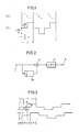
- Fig. 1 is a diagram for explaining a ⁇ /2-DSK signal
- Fig. 2 is a diagram showing a T/2 (T: 1 time slot) differential detector
- Fig. 3 is a diagram showing the relation between a D wave and a U wave
- Fig. 4 is a diagram showing demodulation outputs in sections b and d and a section c in the ⁇ /2-DSK signal.
- the ⁇ /2-DSK signal shown in Fig. 1 is such that the phase of a carrier wave is shifted by + ⁇ /2 during a period of T/2 in the first half of a time slot and further by ⁇ /2 during a period of T/2 in the second half thereof clockwise or counterclockwise, in correspondence to a digital binary information symbol.
- a T/2 delay circuit shown in Fig. 2 is employed.
- the ⁇ /2-DSK signal is applied to an input terminal 1
- the ⁇ /2-DSK signal is applied to a T/2 delay circuit 3a and a multiplier 2.
- An output of the multiplier 2 is outputted through a low pass filter 4 to an output terminal 5.
- the ⁇ /2-DSK signal is such that the phase of the carrier wave is shifted by + ⁇ /2 during a period of T/2 in the first half and further by + ⁇ /2 during a period of T/2 in the second half with respect to a binary information symbol "1", while the phase of the carrier wave is shifted by - ⁇ /2 during a period of T/2 in the first half and further by - ⁇ /2 during a period of T/2 in the second half with respect to a binary information symbol "0".
- a demodulation output e(t) is represented by the following expressions: where cos ⁇ /2 is referred to as the amplitude coefficient, ⁇ represents the relative amplitude ratio of the U wave to the D wave and ⁇ represents the carrier phase difference between the D wave and the U wave.
- cos ⁇ /2 is referred to as the amplitude coefficient
- ⁇ represents the relative amplitude ratio of the U wave to the D wave
- ⁇ represents the carrier phase difference between the D wave and the U wave.
- the demodulation outputs in the sections b and d and in the section c are in compensating relation with respect to the change of the carrier phase difference ⁇ , so that one is decreased while the other is increased.
- the bit error rate is remarkably improved, as compared with the BPSK signal.
- the phase is shifted per 1/2 time slot, the bandwidth of a signal expands, which has presented a problem especially in application to a communication system in which the bandwidth of transmission media must be strictly limited.
- a primary object of the present invention is to provide a digital communication system in which expansion of the bandwidth at the identical transmission rate can be controlled at a low level.
- the present invention is concerned with a digital communication system employing a signal which shifts the carrier phase in correspondence to a digital information symbol, where the digital information symbol is multi-valued and the corresponding phase shift is performed in double steps per time slot in correspondence to each multi-valued information symbol.
- the phase shift per unit time in the case of the identical transmission rate can be decreased to 1/n, as compared with a ⁇ /2-DSK system, so that expansion of the bandwidth can be decreased to 1/n.
- the multi-valued information symbol is a quaternary information symbol (11, 01, 00, 10) and the phase shift per 1/2 time slot corresponding to the quaternary information symbol is represented by ( ⁇ /4, (3/4) ⁇ , (5/4) ⁇ , (7/4) ⁇ ).
- Fig. 5 is a diagram for explaining a quaternary DSK signal employed in an embodiment of the present invention
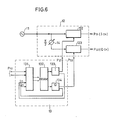
- Fig. 6 is a schematic block diagram showing an example of a quaternary DSK signal generator for generating the quaternary DSK signal.
- a carrier wave signal generator 11 generates a carrier wave signal, the carrier wave signal being applied to an I ⁇ Q modulator 12.
- the I ⁇ Q modulator 12 comprises a ⁇ /2 phase shifter 121, an I CH switching circuit 122 and a Q CH switching circuit 123.
- the ⁇ /2 phase shifter 121 shifts, by ⁇ /2 rad, the phase of a carrier wave applied from the carrier wave signal generator 11.
- the I CH switching circuit 122 switches an I CH carrier wave into the phase 0, the phase ⁇ or the amplitude 0 in correspondence to an I CH modulating signal applied through a terminal P21.
- the Q CH switching circuit 123 switches a Q CH carrier wave into the phase 0, the phase ⁇ or the amplitude 0 in correspondence to a Q CH modulating signal applied through a terminal P22.
- the I CH switching circuit 122 and the Q CH switching circuit 123 comprise a double-balanced modulator, in which the I CH carrier wave is controlled such that it is the phase 0 at +1, the phase ⁇ at -1 and the amplitude 0 at 0.
- the quaternary DSK signal generator further comprises a modulating signal generator 13.
- the modulating signal generator 13 comprises an address generator 131, a RAM 132, an I CH driver 133 and a Q CH driver 134.
- the address generator 131 generates an addressing signal showing how the I CH switching circuit 122 and the Q CH switching circuit 123 are to be controlled, in response to a quaternary information signal applied through a terminal P10 and based on the control state of the above described I CH switching circuit 122 and the Q CH switching circuit 123 corresponding to the preceding quaternary information signals.
- the RAM 132 is addressed by the addressing signal generated in the address generator 131. Instructions stored in advance in the RAM 132 are read out in response to the addressing signal applied from the address generator.
- the I CH driver 133 and the Q CH driver 134 convert the instructions read out from the RAM 132 in the form of control signals required for the above described I CH switching circuit 122 and the Q CH switching circuit 123.
- the amount of phase shift per 1/2 time slot corresponding to each quaternary information symbol is selected as shown in Fig. 5B and the phase shift of the carrier wave corresponding to a quaternary information signal (11, 10, 01, 10, 00, 11) shown in Fig. 5A(a) is shown in Fig. 5A(b).
- Such a signal is generated by forming orthogonal signals (the I CH carrier wave and the Q CH carrier wave) in the following manner. More specifically, in Fig. 5B, if a quaternary information symbol "11" is inputted when the I CH carrier wave is the phase 0 and the Q CH carrier wave is the amplitude 0, the carrier wave is controlled such that the I CH carrier wave remains in the phase 0 and the Q CH carrier wave changes from the amplitude 0 to the phase 0 in the first period of 1/2 time slot, and the I CH carrier wave changes from the phase 0 to the amplitude 0 and the Q CH carrier wave remains in the phase 0 in the second period of 1/2 time slot.
- the I CH carrier wave and the Q CH carrier wave thus obtained are combined.
- Fig. 5B if a quaternary information symbol "11" is inputted when the I CH carrier wave is the phase 0 and the Q CH carrier wave is the amplitude 0, the carrier wave is controlled such that the I CH carrier wave remains in the phase 0 and the Q CH carrier wave
- the carrier wave is controlled such that the I CH carrier wave changes from the amplitude 0 to the phase ⁇ and Q CH carrier wave remains in the amplitude 0 in the first period of 1/2 time slot, and the I CH carrier wave remains in the phase ⁇ and the Q CH carrier wave changes from the phase ⁇ to the amplitude 0 in the second period of 1/2 time slot.
- the I CH carrier wave and the Q CH carrier wave corresponding to the quaternary information symbols in the preceding adjacent time slots are the phase ⁇ or the amplitude 0, and how the phases of the I CH carrier wave and the Q CH carrier wave in the present time slot are to be changed by the quaternary information symbol of the present time slot.
- the carrier wave signal generated from the carrier wave signal generator 11 is applied to the I CH switching circuit 122, and the Q CH switching circuit 123 with the phase shifted, by ⁇ /2 rad, by the ⁇ /2 phase shifter 121.
- the RAM 132 is addressed by the addressing signal from the address generator 131, so that the instructions for controlling the I CH switching circuit 122 and the Q CH switching circuit 123 are read out from the RAM 132.
- the I CH driver 133 and the Q CH driver 134 control the I CH switching circuit 122 and the Q CH switching circuit 123 in response to the instructions.
- the address generator 131 generates the addressing signal in response to the quaternary information symbol in the present time slot and signals from the I CH driver 133 and the Q CH driver 134 in the preceding time slots, so that a memory cell in the RAM 132 corresponding to the addressing signal is addressed.
- the RAM 132 stores in advance the quaternary information symbol in the present time slot and signals to be generated from the I CH driver 133 and the Q CH driver 134 in response to the I CH carrier wave and the Q CH carrier wave in the preceding time slots.
- the RAM 132 outputs the signals based on the instructions and applies the same to the I CH driver 133 and the Q CH driver 134.
- the I CH driver 133 controls the I CH switching circuit 122 and the Q CH driver 134 controls the Q CH switching circuit 123, so that the predetermined I CH carrier wave and Q CH carrier wave are obtained.
- Fig. 7 is a schematic block diagram showing an example of a T/2 delay circuit for demodulating a multi-valued DSK signal generated.
- the multi-valued DSK signal inputted to an input terminal 1 is applied to a T/2 delay circuit 3b, a multiplier 2a for I CH and a multiplier 2b for Q CH .
- the T/2 delay circuit 3b delays, by T/2, the multi-valued DSK signal, the output of the T/2 delay circuit 3b being applied to a first phase shifter 3c and a second phase shifter 3d.
- the second phase shifter 3d applies the amount of phase shift which is larger, by ⁇ /2 rad, than that of the first phase shifter 3c.
- the multiplier 2a for I CH multiplies the output of the T/2 delay circuit 3b by the multi-valued DSK signal, the product being outputted to an output terminal 5a through a low pass filter 4a as the I CH carrier wave.
- the multiplier 2b for Q CH multiplies the output of the second phase shifter 3d by the multi-valued DSK signal, the product being outputted to an output terminal 5b through the low pass filter 4b as the Q CH carrier wave.
- the first phase shifter 3c and the second phase shifter 3d are adjusted such that the phase difference between signals outputted from the T/2 delay circuits 3b in the I CH multiplier 2a and the Q CH multiplier 2b is ⁇ /2 rad, resulting in the respective operations of the multipliers 2a and 2b having orthogonal relation.
- the upper half and the lower half of the circuit shown in Fig. 7 constitute the T/2 differential detectors, respectively, which are responsive to signals out of phase by ⁇ /2 rad in operation thereof.
- a signal obtained in the upper half of the circuit shown in Fig. 7 corresponds to an input signal which is delayed, by ⁇ /2 rad, from a signal obtained in the lower half.
- the signal obtained in the upper half corresponds to a signal of an I axis shown in Fig. 5B and the signal obtained in the lower half corresponds to a signal of the Q axis shown in Fig. 5B.
- the quaternary information symbol is obtained from change in the I CH carrier wave and the Q CH carrier wave in the first half and the second half of a time slot.
- multi-valued (more than quaternary) information symbol can be used.
- the digital information is represented by the multi-valued information symbol and the phase shift corresponding to each multi-valued information symbol is performed two times per 1/2 time slot in correspondence to each multi-valued information symbol, the effect of a DSK communication system can be obtained while controlling expansion of the bandwidth.
Landscapes
- Engineering & Computer Science (AREA)
- Computer Networks & Wireless Communication (AREA)
- Signal Processing (AREA)
- Digital Transmission Methods That Use Modulated Carrier Waves (AREA)
Abstract
Description
- The present invention relates to a digital communication system. More particularly, it relates to a digital communication system employed in mobile radio communication which is immune from multipath interference.
- The inventors proposed "A MODULATION TECHNIQUE SUFFERING FROM LESS TIMING FLUCTUATION OF EYE PATTERNS IN MULTIPATH FADING", in a technical meeting sponsored by the Institute of Electronics and Communication Engineers in Japan held in August 30, 1984. This article describes a DSK (Double Phase Shift Keying) of a type in which a phase is shifted every hlaf time slot by π/2. However, an amount of phase-shift is not limited to π/2, but any amount Δϑ/2 may be taken, which is referred to as "Δϑ/2-DSK".
- Fig. 1 is a diagram for explaining a Δϑ/2-DSK signal, Fig. 2 is a diagram showing a T/2 (T: 1 time slot) differential detector, Fig. 3 is a diagram showing the relation between a D wave and a U wave, and Fig. 4 is a diagram showing demodulation outputs in sections b and d and a section c in the Δϑ/2-DSK signal.
- The Δϑ/2-DSK signal shown in Fig. 1 is such that the phase of a carrier wave is shifted by + Δϑ/2 during a period of T/2 in the first half of a time slot and further by Δϑ/2 during a period of T/2 in the second half thereof clockwise or counterclockwise, in correspondence to a digital binary information symbol. In order to demodulate an original binary information data from the Δϑ/2-DSK signal shown in Fig. 1, a T/2 delay circuit shown in Fig. 2 is employed. In Fig. 2, the Δϑ/2-DSK signal is applied to an
input terminal 1, and the Δϑ/2-DSK signal is applied to a T/2delay circuit 3a and amultiplier 2. An output of themultiplier 2 is outputted through alow pass filter 4 to anoutput terminal 5. - Referring now to Figs. 1 and 2, description is made on operation of a demodulator. The Δϑ/2-DSK signal is such that the phase of the carrier wave is shifted by +Δϑ/2 during a period of T/2 in the first half and further by +Δϑ/2 during a period of T/2 in the second half with respect to a binary information symbol "1", while the phase of the carrier wave is shifted by -Δϑ/2 during a period of T/2 in the first half and further by -Δϑ/2 during a period of T/2 in the second half with respect to a binary information symbol "0".
- Description is now made on operation of multipath reception which presents a problem in mobile radio. Assuming thatis an arrival time difference between the D wave and the U wave which are the Δϑ/2-DSK signals having the identical content and received through two routes having different propagation path lengths, the relation is shown in Fig. 3. Even when the D wave and the U wave are out-of-phase and cancel with each other in sections b and d, the phase difference between the D and U waves in the section c is Δϑ/2, thus the resultant of the D and U waves is not canceled.

- When a combined wave of the D wave and the U wave having such a relation is demodulated in the T/2 differential detector shown in Fig. 2, a demodulation output e(t) is represented by the following expressions:


- As seen from Fig. 4, in the Δϑ/2-DSK signal, the demodulation outputs in the sections b and d and in the section c are in compensating relation with respect to the change of the carrier phase difference φ, so that one is decreased while the other is increased.
- More specifically, in a simple BPSK (Binary Phase Shift Keying) signal, when the phase difference φ between the D wave and the U wave approaches to π(rad), the demodulation output is reduced so that a bit error occurs, while in the φπ/2-DSK signal, even if the phase difference φ takes on π(rad), the demodulation signal does not drop. As a result, the bit error rate is extremely reduced.
- Since the Δϑ/2-DSK signal is constructed as described above, the bit error rate is remarkably improved, as compared with the BPSK signal. However, since the phase is shifted per 1/2 time slot, the bandwidth of a signal expands, which has presented a problem especially in application to a communication system in which the bandwidth of transmission media must be strictly limited.
- Therefore, a primary object of the present invention is to provide a digital communication system in which expansion of the bandwidth at the identical transmission rate can be controlled at a low level.
- Briefly stated, the present invention is concerned with a digital communication system employing a signal which shifts the carrier phase in correspondence to a digital information symbol, where the digital information symbol is multi-valued and the corresponding phase shift is performed in double steps per time slot in correspondence to each multi-valued information symbol.
- Therefore, in accordance with the present invention, if the digital information is multi-valued to m-ary symbol where m = 2n (n: integer), the phase shift per unit time in the case of the identical transmission rate can be decreased to 1/n, as compared with a Δϑ/2-DSK system, so that expansion of the bandwidth can be decreased to 1/n.
- According to a preferred embodiment of the present invention, the multi-valued information symbol is a quaternary information symbol (11, 01, 00, 10) and the phase shift per 1/2 time slot corresponding to the quaternary information symbol is represented by (π/4, (3/4)π, (5/4)π, (7/4)π).
- These objects and other objects, features, aspects and advantages of the present invention will become more apparent from the following detailed description of the present invention when taken in conjunction with the accompanying drawings.
-
- Fig. 1 is a diagram for explaining a Δϑ/2-DSK signal;
- Fig. 2 is a block diagram showing a T/2 differential detector;
- Fig. 3 is a diagram showing the relation between a D wave and an U wave;
- Fig. 4 is a diagram showing demodulation outputs in sections b and d and a section c of the Δϑ/2-DSK signal;
- Fig. 5 is a diagram for explaining a quaternary DSK signal according to an embodiment of the present invention;
- Fig. 6 is a schematic block diagram showing an example of a quaternary DSK signal generator for generating the quaternary DSK signal; and
- Fig. 7 is a schematic block diagram showing a structure of a T/2 delay circuit for demodulating a multi-valued DSK signal.
- Fig. 5 is a diagram for explaining a quaternary DSK signal employed in an embodiment of the present invention, and Fig. 6 is a schematic block diagram showing an example of a quaternary DSK signal generator for generating the quaternary DSK signal.
- Referring now to Fig. 6, description is made on a structure of the quaternary DSK signal generator. A carrier
wave signal generator 11 generates a carrier wave signal, the carrier wave signal being applied to an I·Q modulator 12. The I·Q modulator 12 comprises a π/2 phase shifter 121, an ICH switching circuit 122 and a QCH switching circuit 123. The π/2 phase shifter 121 shifts, by π/2 rad, the phase of a carrier wave applied from the carrierwave signal generator 11. The ICH switchingcircuit 122 switches an ICH carrier wave into thephase 0, the phase π or theamplitude 0 in correspondence to an ICH modulating signal applied through a terminal P₂₁. The QCH switching circuit 123 switches a QCH carrier wave into thephase 0, the phase π or theamplitude 0 in correspondence to a QCH modulating signal applied through a terminal P₂₂. - As an example, the ICH switching
circuit 122 and the QCH switching circuit 123 comprise a double-balanced modulator, in which the ICH carrier wave is controlled such that it is thephase 0 at +1, the phase π at -1 and theamplitude 0 at 0. - The quaternary DSK signal generator further comprises a modulating
signal generator 13. The modulatingsignal generator 13 comprises anaddress generator 131, aRAM 132, an ICH driver 133 and a QCH driver 134. Theaddress generator 131 generates an addressing signal showing how the ICH switching circuit 122 and the QCH switching circuit 123 are to be controlled, in response to a quaternary information signal applied through a terminal P₁₀ and based on the control state of the above described ICH switchingcircuit 122 and the QCH switching circuit 123 corresponding to the preceding quaternary information signals. TheRAM 132 is addressed by the addressing signal generated in theaddress generator 131. Instructions stored in advance in theRAM 132 are read out in response to the addressing signal applied from the address generator. The ICHdriver 133 and the QCH driver 134 convert the instructions read out from theRAM 132 in the form of control signals required for the above described ICH switchingcircuit 122 and the QCH switching circuit 123. - Description is now made on operation. According to an embodiment of the present invention, the amount of phase shift per 1/2 time slot corresponding to each quaternary information symbol is selected as shown in Fig. 5B and the phase shift of the carrier wave corresponding to a quaternary information signal (11, 10, 01, 10, 00, 11) shown in Fig. 5A(a) is shown in Fig. 5A(b).
- Such a signal is generated by forming orthogonal signals (the ICH carrier wave and the QCH carrier wave) in the following manner. More specifically, in Fig. 5B, if a quaternary information symbol "11" is inputted when the ICH carrier wave is the
phase 0 and the QCH carrier wave is theamplitude 0, the carrier wave is controlled such that the ICH carrier wave remains in thephase 0 and the QCH carrier wave changes from theamplitude 0 to thephase 0 in the first period of 1/2 time slot, and the ICH carrier wave changes from thephase 0 to theamplitude 0 and the QCH carrier wave remains in thephase 0 in the second period of 1/2 time slot. The ICH carrier wave and the QCH carrier wave thus obtained are combined. In Fig. 5B, if the quaternary information symbol "11" is inputted when the ICH carrier wave is theamplitude 0 and the QCH carrier wave is thephase 0, the carrier wave is controlled such that the ICH carrier wave changes from theamplitude 0 to the phase π and QCH carrier wave remains in theamplitude 0 in the first period of 1/2 time slot, and the ICH carrier wave remains in the phase π and the QCH carrier wave changes from the phase π to theamplitude 0 in the second period of 1/2 time slot. - Thus, it is temporarily determined whether the ICH carrier wave and the QCH carrier wave corresponding to the quaternary information symbols in the preceding adjacent time slots are the phase π or the
amplitude 0, and how the phases of the ICH carrier wave and the QCH carrier wave in the present time slot are to be changed by the quaternary information symbol of the present time slot. - More specifically, the carrier wave signal generated from the carrier
wave signal generator 11 is applied to the ICH switching circuit 122, and the QCH switching circuit 123 with the phase shifted, by π/2 rad, by the π/2 phase shifter 121. On the other hand, theRAM 132 is addressed by the addressing signal from theaddress generator 131, so that the instructions for controlling the ICH switching circuit 122 and the QCH switching circuit 123 are read out from theRAM 132. The ICH driver 133 and the QCH driver 134 control the ICH switching circuit 122 and the QCH switching circuit 123 in response to the instructions. - More specifically, the
address generator 131 generates the addressing signal in response to the quaternary information symbol in the present time slot and signals from the ICH driver 133 and the QCH driver 134 in the preceding time slots, so that a memory cell in theRAM 132 corresponding to the addressing signal is addressed. TheRAM 132 stores in advance the quaternary information symbol in the present time slot and signals to be generated from the ICH driver 133 and the QCH driver 134 in response to the ICH carrier wave and the QCH carrier wave in the preceding time slots. TheRAM 132 outputs the signals based on the instructions and applies the same to the ICH driver 133 and the QCH driver 134. The ICH driver 133 controls the ICH switching circuit 122 and the QCH driver 134 controls the QCH switching circuit 123, so that the predetermined ICH carrier wave and QCH carrier wave are obtained. - Fig. 7 is a schematic block diagram showing an example of a T/2 delay circuit for demodulating a multi-valued DSK signal generated. In Fig. 7, the multi-valued DSK signal inputted to an
input terminal 1 is applied to a T/2delay circuit 3b, amultiplier 2a for ICH and amultiplier 2b for QCH. The T/2delay circuit 3b delays, by T/2, the multi-valued DSK signal, the output of the T/2delay circuit 3b being applied to afirst phase shifter 3c and asecond phase shifter 3d. Thesecond phase shifter 3d applies the amount of phase shift which is larger, by π/2 rad, than that of thefirst phase shifter 3c. Themultiplier 2a for ICH multiplies the output of the T/2delay circuit 3b by the multi-valued DSK signal, the product being outputted to anoutput terminal 5a through alow pass filter 4a as the ICH carrier wave. On the other hand, themultiplier 2b for QCH multiplies the output of thesecond phase shifter 3d by the multi-valued DSK signal, the product being outputted to anoutput terminal 5b through thelow pass filter 4b as the QCH carrier wave. - The
first phase shifter 3c and thesecond phase shifter 3d are adjusted such that the phase difference between signals outputted from the T/2delay circuits 3b in the ICH multiplier 2a and the QCH multiplier 2b is π/2 rad, resulting in the respective operations of themultipliers - Description is now made on operation of the circuit shown in Fig. 7. A signal obtained in the upper half of the circuit shown in Fig. 7 corresponds to an input signal which is delayed, by π/2 rad, from a signal obtained in the lower half. Thus, the signal obtained in the upper half corresponds to a signal of an I axis shown in Fig. 5B and the signal obtained in the lower half corresponds to a signal of the Q axis shown in Fig. 5B. As a result, the quaternary information symbol is obtained from change in the ICH carrier wave and the QCH carrier wave in the first half and the second half of a time slot.
- Although only an embodiment corresponding to the quaternary information symbol is described, according to the present invention, multi-valued (more than quaternary) information symbol can be used.
- As described in the foregoing, since in the digital communication system according to the present invention, the digital information is represented by the multi-valued information symbol and the phase shift corresponding to each multi-valued information symbol is performed two times per 1/2 time slot in correspondence to each multi-valued information symbol, the effect of a DSK communication system can be obtained while controlling expansion of the bandwidth.
- Although the present invention has been described and illustrated in detail, it is clearly understood that the same is by way of illustration and example only and is not to be taken by way of limitation, the spirit and scope of the present invention being limited only by the terms of the appended claims.
Claims (3)
means for providing said digital information represented by multi-valued information symbols; and
means for shifting the phase corresponding to each multi-valued information symbol two times per time slot in correspondence to each multi-valued information symbol.
said multi-valued information symbol is a quaternary information symbol (11, 01, 00, 10), and
the phase shift per 1/2 time slot corresponding to said quaternary information symbol (11, 01, 00, 10) is represented by (π/4, 3/4π, 5/4π, 7/4 ).
carrier wave signal generating means for generating a carrier wave signal,
means for switching the phase of the carrier wave signal generated from said carrier wave signal generating means into the phase 0 or the phase π and applying to the carrier wave the phase shift corresponding to the quaternary information symbol of said digital information, and
control signal generating means for generating a control signal for switching said switching means in correspondence to said digital information.
Applications Claiming Priority (2)
| Application Number | Priority Date | Filing Date | Title |
|---|---|---|---|
| JP61111673A JPS62265836A (en) | 1986-05-13 | 1986-05-13 | Digital communication system |
| JP111673/86 | 1986-05-13 |
Publications (2)
| Publication Number | Publication Date |
|---|---|
| EP0252589A2 true EP0252589A2 (en) | 1988-01-13 |
| EP0252589A3 EP0252589A3 (en) | 1988-03-16 |
Family
ID=14567284
Family Applications (1)
| Application Number | Title | Priority Date | Filing Date |
|---|---|---|---|
| EP87304174A Withdrawn EP0252589A3 (en) | 1986-05-13 | 1987-05-11 | Digital communication system |
Country Status (4)
| Country | Link |
|---|---|
| US (1) | US4841547A (en) |
| EP (1) | EP0252589A3 (en) |
| JP (1) | JPS62265836A (en) |
| CA (1) | CA1269716A (en) |
Cited By (2)
| Publication number | Priority date | Publication date | Assignee | Title |
|---|---|---|---|---|
| WO1999013622A1 (en) * | 1997-09-05 | 1999-03-18 | Ericsson Inc. | Apparatus for providing increased data rates within existing modulation systems |
| WO2006126907A1 (en) * | 2005-05-25 | 2006-11-30 | Ilya Davidovich Zolotarev | Method for transmitting digital messages via telecommunications systems using a multi-position phase shift keying |
Families Citing this family (2)
| Publication number | Priority date | Publication date | Assignee | Title |
|---|---|---|---|---|
| US8417195B2 (en) * | 2005-09-12 | 2013-04-09 | Magellan Technology Pty Limited | Method and apparatus adapted to transmit data |
| RU2677358C1 (en) * | 2018-01-12 | 2019-01-16 | Сергей Александрович Турко | Modulator of discrete signal by time position |
Family Cites Families (4)
| Publication number | Priority date | Publication date | Assignee | Title |
|---|---|---|---|---|
| FR2394921A1 (en) * | 1977-06-13 | 1979-01-12 | Poitevin Jean Pierre | FOUR-PHASE JUMP-SHIFT MODULATOR |
| US4174505A (en) * | 1978-04-26 | 1979-11-13 | Digital Communications Corporation | Directional PSK modulation and demodulation system |
| FR2469063B1 (en) * | 1979-10-31 | 1987-10-23 | Brossard Pierre | BINARY MODULATIONS WITH PHASE DISPLACEMENT AND MODULATORS |
| US4726038A (en) * | 1985-01-22 | 1988-02-16 | Fumio Ikegami | Digital communication system |
-
1986
- 1986-05-13 JP JP61111673A patent/JPS62265836A/en active Pending
-
1987
- 1987-05-08 US US07/047,319 patent/US4841547A/en not_active Expired - Lifetime
- 1987-05-08 CA CA000536724A patent/CA1269716A/en not_active Expired - Lifetime
- 1987-05-11 EP EP87304174A patent/EP0252589A3/en not_active Withdrawn
Non-Patent Citations (2)
| Title |
|---|
| IEEE GLOBAL TELECOMMUNICATIONS CONFERENCE, GLOBECOM'85, New Orleans, 2nd-5th December 1985, vol. 3, pages 36.4.1-36.4.5, IEEE, New York, US; S. YOSHIDA et al.: "A Novel anti-multipath modulation technique dsk" * |
| NATIONAL TELECOMMUNICATIONS CONFERENCE, Washington, DC, 2 7th-29th November 1979, vol. 2, pages 33.5.1-33.5.5, IEEE, New York, US; E.J. NOSSEN et al.: "Unidirectional phase shift keying" * |
Cited By (3)
| Publication number | Priority date | Publication date | Assignee | Title |
|---|---|---|---|---|
| WO1999013622A1 (en) * | 1997-09-05 | 1999-03-18 | Ericsson Inc. | Apparatus for providing increased data rates within existing modulation systems |
| US6118827A (en) * | 1997-09-05 | 2000-09-12 | Ericsson Inc. | Apparatus for providing increased data rates within existing modulation systems |
| WO2006126907A1 (en) * | 2005-05-25 | 2006-11-30 | Ilya Davidovich Zolotarev | Method for transmitting digital messages via telecommunications systems using a multi-position phase shift keying |
Also Published As
| Publication number | Publication date |
|---|---|
| JPS62265836A (en) | 1987-11-18 |
| CA1269716A (en) | 1990-05-29 |
| EP0252589A3 (en) | 1988-03-16 |
| US4841547A (en) | 1989-06-20 |
Similar Documents
| Publication | Publication Date | Title |
|---|---|---|
| EP0232626B1 (en) | Method of digital signal transmission having a low error rate in the presence of multipath transmission | |
| US5285479A (en) | Quadrature modulation circuit | |
| CA1236168A (en) | Digital radio communication system utilizing quadrature modulated carrier waves | |
| US4849990A (en) | Digital communication system | |
| US5550506A (en) | DQPSK demodulator capable of improving a symbol error rate without decreasing a transmission rate | |
| US4397036A (en) | Diversity system | |
| GB2240674A (en) | Demodulator for PI/4 shifted QPSK signal | |
| US4528512A (en) | Timing synchronizing circuit for demodulators | |
| US6198763B1 (en) | Transmitter and receiver for spread-spectrum communication | |
| EP0252589A2 (en) | Digital communication system | |
| EP0613268A2 (en) | Clock recovery circuit in pi/4 shift quadriphase PSK demodulator | |
| EP0246055B1 (en) | Digital communication system | |
| KR19990028800A (en) | Receiver, Demodulator, and Demodulation Method | |
| US4726038A (en) | Digital communication system | |
| US5841815A (en) | Data receiver for correcting a phase of a received phase-modulated signal | |
| US4498050A (en) | Demodulation device for composite PSK-PSK modulated waves | |
| US4631486A (en) | M-phase PSK vector processor demodulator | |
| EP0620666B1 (en) | Differential continuous phase modulation system for multipath environments | |
| EP0982905B1 (en) | Universal PSK modulation apparatus and method | |
| JPH0225306B2 (en) | ||
| JPS6210950A (en) | Digital radio communication system | |
| JPH07177057A (en) | Spread spectrum modulator and/or demodulator | |
| GB2318229A (en) | Costas loop carrier recovery circuit | |
| JP3186663B2 (en) | PSK receiver | |
| JPS6316937B2 (en) |
Legal Events
| Date | Code | Title | Description |
|---|---|---|---|
| PUAI | Public reference made under article 153(3) epc to a published international application that has entered the european phase |
Free format text: ORIGINAL CODE: 0009012 |
|
| AK | Designated contracting states |
Kind code of ref document: A2 Designated state(s): DE FR GB SE |
|
| PUAL | Search report despatched |
Free format text: ORIGINAL CODE: 0009013 |
|
| AK | Designated contracting states |
Kind code of ref document: A3 Designated state(s): DE FR GB SE |
|
| 17P | Request for examination filed |
Effective date: 19880615 |
|
| 17Q | First examination report despatched |
Effective date: 19900626 |
|
| STAA | Information on the status of an ep patent application or granted ep patent |
Free format text: STATUS: THE APPLICATION IS DEEMED TO BE WITHDRAWN |
|
| 18D | Application deemed to be withdrawn |
Effective date: 19910108 |
|
| RIN1 | Information on inventor provided before grant (corrected) |
Inventor name: IKEGAMI, FUMIO Inventor name: TAKEUCHI, TSUTOMU Inventor name: ARIYAVISITAKUL, SIRIKIAT Inventor name: YOSHIDA, SUSUMU |