EP0252451A2 - Substrate of hybrid ic, method of forming a circuit pattern and apparatus of forming the same - Google Patents
Substrate of hybrid ic, method of forming a circuit pattern and apparatus of forming the same Download PDFInfo
- Publication number
- EP0252451A2 EP0252451A2 EP87109606A EP87109606A EP0252451A2 EP 0252451 A2 EP0252451 A2 EP 0252451A2 EP 87109606 A EP87109606 A EP 87109606A EP 87109606 A EP87109606 A EP 87109606A EP 0252451 A2 EP0252451 A2 EP 0252451A2
- Authority
- EP
- European Patent Office
- Prior art keywords
- solution
- substrate
- circuit
- retaining film
- forming
- Prior art date
- Legal status (The legal status is an assumption and is not a legal conclusion. Google has not performed a legal analysis and makes no representation as to the accuracy of the status listed.)
- Withdrawn
Links
Images




Classifications
-
- H—ELECTRICITY
- H05—ELECTRIC TECHNIQUES NOT OTHERWISE PROVIDED FOR
- H05K—PRINTED CIRCUITS; CASINGS OR CONSTRUCTIONAL DETAILS OF ELECTRIC APPARATUS; MANUFACTURE OF ASSEMBLAGES OF ELECTRICAL COMPONENTS
- H05K3/00—Apparatus or processes for manufacturing printed circuits
- H05K3/10—Apparatus or processes for manufacturing printed circuits in which conductive material is applied to the insulating support in such a manner as to form the desired conductive pattern
- H05K3/12—Apparatus or processes for manufacturing printed circuits in which conductive material is applied to the insulating support in such a manner as to form the desired conductive pattern using thick film techniques, e.g. printing techniques to apply the conductive material or similar techniques for applying conductive paste or ink patterns
- H05K3/1241—Apparatus or processes for manufacturing printed circuits in which conductive material is applied to the insulating support in such a manner as to form the desired conductive pattern using thick film techniques, e.g. printing techniques to apply the conductive material or similar techniques for applying conductive paste or ink patterns by ink-jet printing or drawing by dispensing
- H05K3/125—Apparatus or processes for manufacturing printed circuits in which conductive material is applied to the insulating support in such a manner as to form the desired conductive pattern using thick film techniques, e.g. printing techniques to apply the conductive material or similar techniques for applying conductive paste or ink patterns by ink-jet printing or drawing by dispensing by ink-jet printing
-
- H—ELECTRICITY
- H10—SEMICONDUCTOR DEVICES; ELECTRIC SOLID-STATE DEVICES NOT OTHERWISE PROVIDED FOR
- H10W—GENERIC PACKAGES, INTERCONNECTIONS, CONNECTORS OR OTHER CONSTRUCTIONAL DETAILS OF DEVICES COVERED BY CLASS H10
- H10W70/00—Package substrates; Interposers; Redistribution layers [RDL]
- H10W70/01—Manufacture or treatment
- H10W70/05—Manufacture or treatment of insulating or insulated package substrates, or of interposers, or of redistribution layers
- H10W70/098—Applying pastes or inks, e.g. screen printing
-
- H—ELECTRICITY
- H10—SEMICONDUCTOR DEVICES; ELECTRIC SOLID-STATE DEVICES NOT OTHERWISE PROVIDED FOR
- H10W—GENERIC PACKAGES, INTERCONNECTIONS, CONNECTORS OR OTHER CONSTRUCTIONAL DETAILS OF DEVICES COVERED BY CLASS H10
- H10W99/00—Subject matter not provided for in other groups of this subclass
-
- Y—GENERAL TAGGING OF NEW TECHNOLOGICAL DEVELOPMENTS; GENERAL TAGGING OF CROSS-SECTIONAL TECHNOLOGIES SPANNING OVER SEVERAL SECTIONS OF THE IPC; TECHNICAL SUBJECTS COVERED BY FORMER USPC CROSS-REFERENCE ART COLLECTIONS [XRACs] AND DIGESTS
- Y10—TECHNICAL SUBJECTS COVERED BY FORMER USPC
- Y10S—TECHNICAL SUBJECTS COVERED BY FORMER USPC CROSS-REFERENCE ART COLLECTIONS [XRACs] AND DIGESTS
- Y10S428/00—Stock material or miscellaneous articles
- Y10S428/901—Printed circuit
-
- Y—GENERAL TAGGING OF NEW TECHNOLOGICAL DEVELOPMENTS; GENERAL TAGGING OF CROSS-SECTIONAL TECHNOLOGIES SPANNING OVER SEVERAL SECTIONS OF THE IPC; TECHNICAL SUBJECTS COVERED BY FORMER USPC CROSS-REFERENCE ART COLLECTIONS [XRACs] AND DIGESTS
- Y10—TECHNICAL SUBJECTS COVERED BY FORMER USPC
- Y10T—TECHNICAL SUBJECTS COVERED BY FORMER US CLASSIFICATION
- Y10T29/00—Metal working
- Y10T29/49—Method of mechanical manufacture
- Y10T29/49002—Electrical device making
- Y10T29/49117—Conductor or circuit manufacturing
-
- Y—GENERAL TAGGING OF NEW TECHNOLOGICAL DEVELOPMENTS; GENERAL TAGGING OF CROSS-SECTIONAL TECHNOLOGIES SPANNING OVER SEVERAL SECTIONS OF THE IPC; TECHNICAL SUBJECTS COVERED BY FORMER USPC CROSS-REFERENCE ART COLLECTIONS [XRACs] AND DIGESTS
- Y10—TECHNICAL SUBJECTS COVERED BY FORMER USPC
- Y10T—TECHNICAL SUBJECTS COVERED BY FORMER US CLASSIFICATION
- Y10T29/00—Metal working
- Y10T29/49—Method of mechanical manufacture
- Y10T29/49002—Electrical device making
- Y10T29/49117—Conductor or circuit manufacturing
- Y10T29/49124—On flat or curved insulated base, e.g., printed circuit, etc.
-
- Y—GENERAL TAGGING OF NEW TECHNOLOGICAL DEVELOPMENTS; GENERAL TAGGING OF CROSS-SECTIONAL TECHNOLOGIES SPANNING OVER SEVERAL SECTIONS OF THE IPC; TECHNICAL SUBJECTS COVERED BY FORMER USPC CROSS-REFERENCE ART COLLECTIONS [XRACs] AND DIGESTS
- Y10—TECHNICAL SUBJECTS COVERED BY FORMER USPC
- Y10T—TECHNICAL SUBJECTS COVERED BY FORMER US CLASSIFICATION
- Y10T29/00—Metal working
- Y10T29/49—Method of mechanical manufacture
- Y10T29/49002—Electrical device making
- Y10T29/49117—Conductor or circuit manufacturing
- Y10T29/49124—On flat or curved insulated base, e.g., printed circuit, etc.
- Y10T29/4913—Assembling to base an electrical component, e.g., capacitor, etc.
- Y10T29/49144—Assembling to base an electrical component, e.g., capacitor, etc. by metal fusion
-
- Y—GENERAL TAGGING OF NEW TECHNOLOGICAL DEVELOPMENTS; GENERAL TAGGING OF CROSS-SECTIONAL TECHNOLOGIES SPANNING OVER SEVERAL SECTIONS OF THE IPC; TECHNICAL SUBJECTS COVERED BY FORMER USPC CROSS-REFERENCE ART COLLECTIONS [XRACs] AND DIGESTS
- Y10—TECHNICAL SUBJECTS COVERED BY FORMER USPC
- Y10T—TECHNICAL SUBJECTS COVERED BY FORMER US CLASSIFICATION
- Y10T428/00—Stock material or miscellaneous articles
- Y10T428/24—Structurally defined web or sheet [e.g., overall dimension, etc.]
- Y10T428/24802—Discontinuous or differential coating, impregnation or bond [e.g., artwork, printing, retouched photograph, etc.]
- Y10T428/24917—Discontinuous or differential coating, impregnation or bond [e.g., artwork, printing, retouched photograph, etc.] including metal layer
-
- Y—GENERAL TAGGING OF NEW TECHNOLOGICAL DEVELOPMENTS; GENERAL TAGGING OF CROSS-SECTIONAL TECHNOLOGIES SPANNING OVER SEVERAL SECTIONS OF THE IPC; TECHNICAL SUBJECTS COVERED BY FORMER USPC CROSS-REFERENCE ART COLLECTIONS [XRACs] AND DIGESTS
- Y10—TECHNICAL SUBJECTS COVERED BY FORMER USPC
- Y10T—TECHNICAL SUBJECTS COVERED BY FORMER US CLASSIFICATION
- Y10T428/00—Stock material or miscellaneous articles
- Y10T428/25—Web or sheet containing structurally defined element or component and including a second component containing structurally defined particles
-
- Y—GENERAL TAGGING OF NEW TECHNOLOGICAL DEVELOPMENTS; GENERAL TAGGING OF CROSS-SECTIONAL TECHNOLOGIES SPANNING OVER SEVERAL SECTIONS OF THE IPC; TECHNICAL SUBJECTS COVERED BY FORMER USPC CROSS-REFERENCE ART COLLECTIONS [XRACs] AND DIGESTS
- Y10—TECHNICAL SUBJECTS COVERED BY FORMER USPC
- Y10T—TECHNICAL SUBJECTS COVERED BY FORMER US CLASSIFICATION
- Y10T428/00—Stock material or miscellaneous articles
- Y10T428/25—Web or sheet containing structurally defined element or component and including a second component containing structurally defined particles
- Y10T428/254—Polymeric or resinous material
-
- Y—GENERAL TAGGING OF NEW TECHNOLOGICAL DEVELOPMENTS; GENERAL TAGGING OF CROSS-SECTIONAL TECHNOLOGIES SPANNING OVER SEVERAL SECTIONS OF THE IPC; TECHNICAL SUBJECTS COVERED BY FORMER USPC CROSS-REFERENCE ART COLLECTIONS [XRACs] AND DIGESTS
- Y10—TECHNICAL SUBJECTS COVERED BY FORMER USPC
- Y10T—TECHNICAL SUBJECTS COVERED BY FORMER US CLASSIFICATION
- Y10T428/00—Stock material or miscellaneous articles
- Y10T428/25—Web or sheet containing structurally defined element or component and including a second component containing structurally defined particles
- Y10T428/256—Heavy metal or aluminum or compound thereof
-
- Y—GENERAL TAGGING OF NEW TECHNOLOGICAL DEVELOPMENTS; GENERAL TAGGING OF CROSS-SECTIONAL TECHNOLOGIES SPANNING OVER SEVERAL SECTIONS OF THE IPC; TECHNICAL SUBJECTS COVERED BY FORMER USPC CROSS-REFERENCE ART COLLECTIONS [XRACs] AND DIGESTS
- Y10—TECHNICAL SUBJECTS COVERED BY FORMER USPC
- Y10T—TECHNICAL SUBJECTS COVERED BY FORMER US CLASSIFICATION
- Y10T428/00—Stock material or miscellaneous articles
- Y10T428/31504—Composite [nonstructural laminate]
Definitions
- the present invention relates to a substrate of a hybrid IC, a method of forming a circuit pattern by using the substrate and an apparatus for forming the same.
- a screen printing method for example, was used for forming a circuit pattern.
- the prior art method uses a substrate of alumina or similar material with a screen mask formed there, the screen mask having a circuit pattern formed thereon.
- the circuit pattern is formed on the substrate by means of paste which contains material for forming a circuit element. This method is like a mimeograph printing procedure.
- An object of the present invention is to provide a hybrid IC substrate, a method of forming a circuit pattern and an apparatus for forming the same, which is completely different form the prior method.
- a hybrid IC substrate body is coated with a retaining film, and the solution which contains materials for forming a circuit element permeates the retaining film and becomes attached to the hybrid IC substrate. The solution then remains at the point of attachment, being held in position by the retaining film.
- a predetermined pattern is drawn on a hybrid IC substrate using a solution which contains materials for forming a circuit element.
- the solution is baked in an oven.
- the retaining film is thus baked off, thereby leaving a film of materials for forming a circuit element.
- an apparatus for forming a circuit pattern comprising means for storing a solution containing materials for forming a circuit element, a drop-of-liquid expelling means for expelling in drop form the solution stored in the storing means, a substrate placing means for positioning a hybrid IC substrate the surface of which is coated with a retaining film, the retaining film allowing the solution expelled from the drop-of-liquid expelling means to permeate the retaining film at the position at which the solution is attached to the retaining film and also allowing said solution to be retained, means for moving the drop-of-liquid expelling means and said substrate placing means relative to each other, and means for controlling the timing of release of drops of liquid through the drop-of-liquid expelling means and the amount and direction of movement caused by the moving means based on the circuit pattern data, whereby a circuit pattern can be drawn on the hybrid IC substrate by using the solution containing materials for forming a circuit element.
- Figure 1 shows a sectional view of a major part of the hybrid IC formed substrate 1 of a hybrid IC formed in accordance with the present invention.
- the substrate body 2 comprises aluminium oxide, aluminium nitride, silicon nitride, silicon carbide and beryllium oxide, glass, enamel and zirconium oxide, etc.
- the retaining film 3 comprises acrylic resin, for example Seladic 26 (manufactured by Dai Nippon Ink Chemical Industry), and covers the substrate body 2 with a layer of almost constant thickness.
- the retaining film 3, which comprises this acrylic resin, is preferably formed using a spin coater to coat the resin on the substrate body 2 and cause it to dry.
- the resin may be sprayed in a moist form on the substrate body 2, or the substrate body 2 may be dipped into a solution of acrylic resin.
- Any method by which a retaining film 3 of acrylic resin is formed on the substrate body 2 can be employed in the invention. As the film thickness of acrylic resin becomes a main factor in determining the width of a line of a circuit pattern, it should be controlled so as to achieve an optimum value, as will be explained later.
- a paste (manufactured by Engelhard Minerals and Chemicals Corporation) of organic matter containing gold (Au) as a circuit-element forming material, is dissolved in an alpha-terpineol solution (for example, comprising 40% of the above-mentioned paste by weight and 60% of alpha-terpineol by weight and will be referred to as solution I).
- solution I alpha-terpineol solution
- the ink liquid 4 is, as shown in Figure 2A, dropped on a hybrid IC substrate (called a substrate hereinafter) 1 which comprises a substrate body 2 with a retaining film 3 on the upper surface.
- the ink liquid or solution drop 4 falls on the retaining film 3 of the substrate 1.
- the retaining film 3 is dissolved by the alpha-terpineol solvent of the ink liquid 4, as the retaining film 3 is comprised of an acrylic resin.
- the ink liquid 4 is able to permeate through the film 3 to the upper surface of the substrate body 2, and the position of the ink liquid drop 4 is maintained by the retaining film 3, which ensures that it does not spread out in a horizontal direction.
- the reason why the ink liquid 4 is suppressed from spreading in a horizontal direction is that all of the ink liquid 4 is quickly drawn into the retaining film 3 thereby ensuring that the spreading of the ink liquid 4 in a horizontal direction is completed at an early stage.
- Suppression of spreading of the ink liquid drop 4 in a horizontal direction and its permeation through the film 3 is determined by the amount of the ink contacting the retaining film 3 and the thickness of the retaining film 3.
- the thickness of the retaining film 3 is set at a thickness from several thousands of angstroms to several tens of microns and the ink liquid 4 drops are set at a diameter of twenty microns to three hundred microns.
- the substrate body 2 is heated to the appropriate temperature (about 100°C) for the appropriate length of time by a heater.
- the solvent of the ink liquid 4 is thereby quickly evaporated, thus preventing the ink liquid 4 from spreading.
- the substrate 1 is baked in an oven (I.R. oven).
- the temperature of the oven is increased from ambient to a peak temperature (such as 850°C)over a period of about ten minutes and, after the peak temperature is maintained for several minutes, the temperature of the oven is returned to ambient over a period of several minutes.
- the retaining film 3 formed on the substrate body 2 is baked off.
- the remaining liquid part of the ink liquid 4 is thereby evaporated leaving the gold (Au) part of the ink liquid 4, thus forming a circuit pattern made of gold on the substrate body 2 as a metal film 5, as shown in Figure 2D.
- a predetermined circuit pattern is drawn by means of ink drops 4 on the hybrid IC substrate 1 and, when baked, a circuit pattern, consisting of the metal film 5 and having the same pattern as drawn on the substrate 1, is formed.
- the embodiment of the present invention uses the substrate 1 having a retaining film 3 made of acrylic resin (Seladic 26 etc.), which is formed thereon and the ink liquid 4 obtained by dissolving a paste of organic matter including gold (Au) in an alpha-terpineol solution.
- the ink liquid 4 is used only on the part on which a circuit pattern is intended to be drawn or formed and unnecessarily high consumption of the ink liquid 4 is avoided.
- the maintenance and protective properties of the ink liquid 4 are excellent, irregularities in the surface such as concave or convex portions, and curved or wavy portions of the surface of the substrate body 2 do not affect the pattern formation and a hybrid IC of high reliability can be manufactured.
- the hybrid IC substrate 1, having the above characteristic, is also made possible by appropriately selecting the materials of the retaining film 3 and the composition of the ink liquid 4, as will be described below.
- the ink liquid 4 is composed of a chloroform solution in which a paste (manufactured by Engelhard Minerals & Chemicals Corporation) of organic matter including gold (Au) is dissolved, and the solution comprises, for example, 40% of the above mentioned paste by weight and 60% of chloroform by weight, and will be referred to as solution II hereinafter.
- the retaining film 3 may be made of acrylic resin (Seladic 26 etc.) which is dissolved by the chloroform as the solvent so that the ink liquid 4 reaches the surface of the substrate body 2, thereby maintaining its status. Then it can achieve the same effect as the above embodiment.
- the ink liquid 4 is composed of a toluene solution in which a paste (manufactured by Engelhard Minerals & Chemicals Corporation) of organic matter including gold (Au) is dissolved.
- the solution comprises, for example, 40% of the above-mentioned paste by weight and 60% of toluene by weight, and will be referred to as solution III hereinafter.
- the retaining film 3 is composed of acrylic resin such as Seladic 26 or polyvinyl butylal (PVB) such as 3000K (manufactured by Electric Chemical Industry), which can be dissolved by toluene, and maintains a status such that the ink liquid 4 permeates the film 3 and reaches the substrate body 2. These replacements for the film 3 and ink liquid 4 will result in the same effect as in the above described embodiment.
- the ink liquid 4 is composed of a WA-OIL solution (manufactured by Noritake Company Limited), in which a paste (manufactured by Noritake Company Limited) of organic matter including gold (Au) is dissolved, or of a butyl carbitol acetate (BCA) solution.
- the WA-OIL solution comprises, for example, 80% of the above-mentioned paste by weight and 20% of WA-OIL by weight, and will be referred to as solution IV hereinafter.
- the retaining film 3 is composed of an acrylic resin such as Seladic 26 or polyvinyl butylal (PVB) such as 3000K, which is dissolved in WA-OIL or BCA solution and which enables the ink liquid 4 to permeate the retaining film 3 until it reaches the upper surface of the substrate body 2, thereby maintaining its status.
- an acrylic resin such as Seladic 26 or polyvinyl butylal (PVB) such as 3000K
- the ink liquid 4 is composed of a water solution in which a soluble organic material is dissolved and retaining film 3 is composed of a polyvinyl alcohol which is dissolved by the water solution thereby enabling the ink liquid 4 to permeate until it reaches the surface of the substrate body 2.
- the ink liquid maintains a status such that it remains on the substrate body at the position where the ink liquid contacts the substrate body.
- Such modification likewise produces the same effect as the aforementioned embodiments.
- the ink liquid 4 is composed of a solution (comprising, for example, 38.8% of silver neodecanate by weight, 4.85% of palladium diisobutyl dithiocarbamate by weight, 1.5% of copper ethylene diamine bisacetyl acetonate by weight, 27.5% of toluene by weight, and 27.5% of diethylene glycol dimethyl ether by weight, and hereinafter referred to as solution V) obtained by dissolving silver neodecanate (for example Ag 15%), palladium diisobutyl dithio-carbamate (for example Pd 1%) and copper ethylene diamine bisacetyl acetonate (for example Cu 0.3%) in toluene and diethylene glycol dimethyl ether.
- a solution comprising, for example, 38.8% of silver neodecanate by weight, 4.85% of palladium diisobutyl dithiocarbamate by weight, 1.5% of copper ethylene diamine
- the retaining film 3 is composed of an ethyl cellulose 10 c.p.s. (manufactured by Kanto Chemical) or BM-S (Emalex B, manufactured by Sekisui Chemical).
- the present embodiment can achieve the same effect as the above embodiment.
- the ink liquid 4 is composed of a solution (comprising, for example, 36 - 41% of silver neodecanate by weight, 30 - 40% of toluene by weight, and 20 - 30% of alpha-terpineol by weight, and hereinafter referred to as solution VI) obtained by dissolving silver neodecanate (for example Ag 14% to 16%) in toluene and alpha-terpineol.
- the retaining film 3 is composed of an acrylic resin such as Seladic 26 or polyvinyl butylal (PVB) such as 3000K. The present embodiment can achieve the same effect as the above embodiment.
- a retaining film or layer 3 may be a material for allowing a solution, including material (e.g. gold) for forming a circuit element, to permeate therethrough at the position at which the solution contacts the retaining film and for retaining the solution.
- the film or layer 3 may be a retaining film 3 having numerous holes 6. The liquid ink solution permeates and is retained within the holes 6.
- the radius of the hole 6 is sufficient to allow the ink liquid 4 to permeate into the holes and the density of the holes 6 may be appropriately selected, and is determined by the amount of the ink liquid 4 and the thickness of the film 5.
- Such retaining film 3 can be obtained by forming gelatin or cellulose, for example, into a porous material having numerous holes, each having a diameter of less than one thousand angstroms.
- the retaining film 3 which serves as a retaining member for the ink liquid 4 may be formed of a liquid absorbing polymer other than acrylic resin.
- a high molecular absorbing polymer can be used as the liquid absorbing polymer.
- the ink liquid 4 which contains the circuit element forming material is absorbed and retained at a position at which the ink liquid 4 contacts the retaining film 3, thereby providing the same effect as above.
- Au is used as the circuit element forming material.
- Other conductive elements or materials may be used instead, such as Ag, Ag/Pd, Ag/Pt, Au/Pd, Au/Pt, Cu, W, and Pt.
- Resistor materials such as materials including ruthenium (for example, RuO2, Bi2Ru2O7, Pb2Ru2O6, or BaRuO3), materials including silver (for example, Ag/Pd(PdO)) and materials including indium (for example, InO3/SnO2,InO3) may be used.
- Dielectric materials such as a glass paste and resin paste (for example, polyester )may also be used.
- the line width of the circuit pattern formed by the above method has a direct relationship with the film thickness of the retaining film 3.
- the retaining film 3 comprises ethyl cellulose 10 c.p.s. having a film thickness of 0.3 micron and the ink liquid 4 is made of the aforementioned solution V
- a circuit pattern can be drawn with a line width of 180 microns.
- the relationship shown in Figure 4A can be obtained between a film thickness of the retaining film 3 and the line width of the circuit pattern.
- the relationship shown in Figure 4B can be obtained.
- Figure 5 shows schematically the circuit-pattern-forming apparatus 11.
- An X-direction moving support 14, movable from right to left or vice versa, (X-axis direction) is provided on a base support 13 which is mounted on the table 12 of the apparatus 11.
- the X-direction moving support 14 is coupled by a gear to a ball screw which is connected to an X-direction driving stepping motor Mx which is attached to the left surface of the base 13.
- the stepping motor Mx drives the moving support 14 from right to left or vice-versa, i.e. in the X-axis direction.
- a Y-direction moving support 15 is provided on a surface of the X-direction moving support 14 such that it can slide back and forth (in the Y-axis direction).
- the Y-direction moving support 15 is geared to a ball screw 16 which is connected to a Y-direction driving stepping motor My which is attached to the front side of the X-direction moving support 14. This enables the Y-direction driving stepping motor My to rotate in a clockwise and anticlockwise direction, so that the Y-direction moving support 15 is moved backward and forward or in a Y-axis direction.
- a depression or the convex portion 17 is formed on the upper surface of the Y-direction moving support 15.
- a fixed or stationary support 18 made of aluminium is inserted into depression 17 so as to achieve a regular or flat surface equal to the upper surface of said moving support 15.
- the substrate 1 is fixed on the upper surface of the fixed support 18.
- a heater 19 is attached to the lower surface of the fixed support 18 and the substrate is maintained at an appropriate temperature through the fixed support 18.
- a forward extending L-shaped arm 20, is mounted at the rear of table 12.
- An ink jet head 22 which may be called as a liquid nozzle or producer, a liquid ejecting nozzle, a drop-of-liquid expelling device or a liquid spot producing device is provided at the foremost end of the arm 20 such that it is opposed to and faces the upper surface of the fixed support 18.
- the ink jet head 22 is equipped with a tank 21 for holding ink liquid 4 for drawing a circuit pattern, the ink liquid having a paste (manufactured by Engelhard Minerals & Chemicals Corporation) as solute and an alpha-terpineol as the solvent. Such ink liquids 4 are discussed hereinabove.
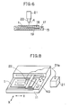
- the ink jet head 22 operates in accordance with control signals from a control apparatus (described below) and the ink liquid 4 transmitted from the tank 21 is directed onto the substrate 1 which is positioned on the top surface of the fixed support 18, as shown in Figure 6.
- a microcomputer 31 coupled to the operation box 23 comprises a central processing unit 32 (which is referred to as CPU hereinafter), a program memory 33 comprising a read only memory (ROM) for storing a control program, a working memory 34 comprising a readable and rewritable memory or random access memory (RAM) for storing results obtained from operational processing and circuit pattern data.
- the CPU 32 performs an operational process in accordance with the control program.
- CPU 32 receives coordinate data transmitted from a CAD system of an external apparatus and stores it in a predetermined memory area of said working memory 34. Based on the coordinate data, data for enabling the ink jet head 22 to draw a circuit pattern by using the ink liquid 4 is operationally processed in the present forming apparatus.
- This circuit pattern data comprises a direction and amount of rotation of a stepping motor Mx for driving in an X-direction and a stepping motor My for driving in a Y-direction and comprises operation timing of the ink jet head 22.
- the CPU 32 controls the X-direction and Y-direction driving stepping motors Mx and My through motor driving circuits 36 and 37 and controls the operation of the ink jet head 22 through a driving circuit 38 for the liquid producer. Instructions for process execution, given to the CPU 32, are made by a key operation of the keyboard 24.
- step 51 coordinate data designating a circuit pattern to be formed by a CAD system 35 is formulated (step 51).
- the CPU 32 receives coordinate data formed by the CAD system 35 in accordance with a key operation on a keyboard 24, stores it in working memory 34 (step 52), and a simultaneously performs an operation process bases on the coordinate data (step 53), thereby forming circuit pattern data such as the driving amount of the motor and the liquid-expelling timing, and stores the data in a different area of the working memory 34 (step 54).
- CPU 32 After the operator fixes the substrate 1 at a predetermined position on the fixed support 18, he operates a start key (not shown) on keyboard 24. In response to ON signals of the start key (step 55), CPU 32 reads the circuit pattern data formed as a result of the operation process from the working memory 34 (step 56), thereby controlling and driving the X and Y direction driving stepping motors Mx and My based on the circuit pattern data and driving the ink jet head 22 (step 57).
- the substrate 1 on the fixed support 18 moves in an X and Y direction relative to the ink jet head 22 so that the ink jet head 22 can draw the circuit pattern by ejection of the ink liquid 4.
- the ink jet head 22 produces the ink liquid 4, thereby enabling the circuit pattern formed by the CAD system 35 to be drawn on the substrate 1.
- the retaining film 3 allows the ink liquid 4 to permeate and/or dissolve through the film 3 onto the substrate body 2 at the position of the production of the liquid and maintains the status of the liquid 4 without spreading of the liquid 4 in a horizontal direction.
- the solution of the ink liquid 4 is rapidly evaporated, thereby completely preventing the ink liquid 4 from spreading.
- the following new pattern is drawn on the pattern previously drawn, in the same manner as described above, after the ink liquid 4 is changed to one containing a different circuit-element-forming material.
- the substrate 1 is baked in an oven.
- the retaining film 3 formed on the substrate body 2 is baked off and the ink liquid 4 is resolved or decomposited, thereby enabling the solvent of the ink liquid 4 to be evaporated, and leaving the circuit-element-forming material on the substrate 1, as shown in Figure 2D.
- the circuit-element -forming material i.e. a conductor such as Au
- the present embodiment makes it possible to draw a circuit pattern on the substrate 1 with ease merely by operating the formation apparatus 11 based on a circuit pattern formed by, for example, a CAD system in advance.
- the pattern can be directly formed on the substrate 1, a screen mask is not necessary, unlike the prior screen printing method.
- the great amount of expense and time which was formerly spent in manufacturing a mask can be saved and high speed drawing of the pattern becomes possible, thereby achieving a more highly automated system.
- the ink liquid 4 can be formed on an extremely small spot by the ink jet head 22, an extremely fine micro-pattern can be formed. Further, as only the necessary amount of the ink liquid 4 is used, this invention can achieve a great amount of cost reduction as compared to the screen printing method in which much of the paste is wasted.
- Concave and convex portions of a pattern surface, which inevitably occur in a screen mesh, are not formed by the present invention, thereby enabling the formation of a low noise circuit.
- a glass (insulating) layer is printed on a lower conductor and an upper conductor is formed thereon, thereby providing two-layer construction.
- insulating layer which can cause a short circuit between lower and upper conductors.
- the interval between liquid drops sequentially expelled from the ink jet head 22 is controlled or the number of drops is made to have a large density thereby preventing a pin hole from occurring even in the case of a single drawing of the pattern.
- the ink jet head 22 as shown in Figure 8, can be attached to a moving arm 40 which is movable in the Y-direction along slot 111 of table 11 and which is also movable in the Xdirection perpendicular to the Y-direction in slot 111, and the ink jet head 22 can be moved in a controlled manner relative to the substrate 1, thereby drawing a circuit pattern.
- the liquid spot producing apparatus 22 can be moved with more ease, thereby achieving a high speed in drawing the circuit pattern.
- a tank 21 is coupled with the ink jet head 22.
- the tank 21, as shown in Figure 8 can be provided at an external position and the ink liquid 4 in the tank 21 can be supplied to the ink jet head 22 through a tube 21a.
- the ink jet head 22 is not limited to a special type but may be made similar to an ink jet head such as that used for a printer of an ink jet type and/or may use an appropriate head such as a piezo electric head type ink jet head or a heat ink jet head, or the like.
- a control computer 41 may be, as shown in Figure 8, provided between the CAD 35 and CPU 32, thereby receiving all of the data from CAD 35 in a batch and then transmitting the data to CPU 32 of the main apparatus 11 successively.
- the pattern data may be stored in an external data storing apparatus such as a floppy disc and may be read from the floppy disc for the purpose of an actual operation of the pattern data.
- the forming apparatus 11 of the above embodiments is provided with the ink jet head 22.
- a plurality of liquid spot producing devices i.e. nozzles
- different ink jet heads 22 can be used, for example, for circuit element forming materials such as conductor material, resistor material and dielectric material respectively.
- the ink jet head 22 are attached to the arm 20 or the moving arm 40 respectively.
- These circuit-element-formation materials are appropriately selected by the control circuit to be drawn as respective patterns on the film 3, so as to eliminate the necessity for changing the ink jet head 22 to new ones each time a different pattern is formed. This enables successive patterns to be formed on the substrate 1 and therefore allows the patterns to be formed in a shorter time period.
- different tanks 21 may be provided at the end of the arm 20, or instead, as shown in Figure 11, different tanks 21 can be provided at different positions, and the ink liquid 4 may be applied to the corresponding ink jet head 22 through the tubes 21a respectively.
- the present invention forms the circuit pattern on the substrate in a way very different from the prior art and also the present invention can provide a circuit pattern at a very low cost, in a short time period, and a high precision.
Landscapes
- Engineering & Computer Science (AREA)
- Manufacturing & Machinery (AREA)
- Microelectronics & Electronic Packaging (AREA)
- Manufacturing Of Printed Wiring (AREA)
- Non-Metallic Protective Coatings For Printed Circuits (AREA)
Abstract
Description
- The present invention relates to a substrate of a hybrid IC, a method of forming a circuit pattern by using the substrate and an apparatus for forming the same.
- In the prior art, a screen printing method, for example, was used for forming a circuit pattern. The prior art method uses a substrate of alumina or similar material with a screen mask formed there, the screen mask having a circuit pattern formed thereon. The circuit pattern is formed on the substrate by means of paste which contains material for forming a circuit element. This method is like a mimeograph printing procedure.
- However, this prior screen printing method requires many screen masks to form a complete circuit and a large amount of time to design and manufacture the screen masks. In addition, much of the paste attached to the screen mask or squeeze is disposed of. Therefore, a large quantity of the expensive paste is wasted.
- An object of the present invention is to provide a hybrid IC substrate, a method of forming a circuit pattern and an apparatus for forming the same, which is completely different form the prior method.
- According to a first feature of the present invention, a hybrid IC substrate body is coated with a retaining film, and the solution which contains materials for forming a circuit element permeates the retaining film and becomes attached to the hybrid IC substrate. The solution then remains at the point of attachment, being held in position by the retaining film.
- In a second feature of the present invention, a predetermined pattern is drawn on a hybrid IC substrate using a solution which contains materials for forming a circuit element. After the solution has permeated the retaining film and become attached to the substrate's surface, the substrate is baked in an oven. The retaining film is thus baked off, thereby leaving a film of materials for forming a circuit element.
- According to a third feature of the present invention, there is provided an apparatus for forming a circuit pattern comprising means for storing a solution containing materials for forming a circuit element, a drop-of-liquid expelling means for expelling in drop form the solution stored in the storing means, a substrate placing means for positioning a hybrid IC substrate the surface of which is coated with a retaining film, the retaining film allowing the solution expelled from the drop-of-liquid expelling means to permeate the retaining film at the position at which the solution is attached to the retaining film and also allowing said solution to be retained, means for moving the drop-of-liquid expelling means and said substrate placing means relative to each other, and means for controlling the timing of release of drops of liquid through the drop-of-liquid expelling means and the amount and direction of movement caused by the moving means based on the circuit pattern data, whereby a circuit pattern can be drawn on the hybrid IC substrate by using the solution containing materials for forming a circuit element.
-
- Figure 1 is a sectional view of a portion of a hybrid IC substrate for use in the present invention,
- Figure 2A to 2D are views which explain the process of forming a metal film on the substrate,
- Figure 3 is a front view of the main part of a different example of a retaining film used in another embodiment of the present invention,
- Figure 4A and 4B are graphic diagrams showing one example of the relationship between the line width of a circuit pattern formed by the method of the present invention and the film thickness of the retaining film,
- Figure 5 is a perspective view of a forming apparatus according to the present invention,
- Figure 6 is a sectional view of a moving support for use in the forming apparatus of Figure 5,
- Figure 7 is a block diagram of an electrical circuit of a forming apparatus of the present invention,
- Figure 8 is a perspective view of the forming apparatus according to another embodiment of the present invention,
- Figure 9 is a block diagram of the electrical circuit of another embodiment of the present invention,
- Figures 10 and 11 are perspective views of a main part of the forming apparatus which includes a plurality of devices for applying ink solution onto the hybrid IC substrate, and
- Figure 12 is a flow chart showing a control operation of the forming apparatus shown in Figure 5.
- Figure 1 shows a sectional view of a major part of the hybrid IC formed
substrate 1 of a hybrid IC formed in accordance with the present invention. Thesubstrate body 2 comprises aluminium oxide, aluminium nitride, silicon nitride, silicon carbide and beryllium oxide, glass, enamel and zirconium oxide, etc. Aretaining film 3, which allows a later explainedink liquid 4 to permeate therethrough and be retained therein, is formed on the surface of thesubstrate body 2. Theretaining film 3 comprises acrylic resin, for example Seladic 26 (manufactured by Dai Nippon Ink Chemical Industry), and covers thesubstrate body 2 with a layer of almost constant thickness. Theretaining film 3, which comprises this acrylic resin, is preferably formed using a spin coater to coat the resin on thesubstrate body 2 and cause it to dry. Alternatively, the resin may be sprayed in a moist form on thesubstrate body 2, or thesubstrate body 2 may be dipped into a solution of acrylic resin. Any method by which aretaining film 3 of acrylic resin is formed on thesubstrate body 2 can be employed in the invention. As the film thickness of acrylic resin becomes a main factor in determining the width of a line of a circuit pattern, it should be controlled so as to achieve an optimum value, as will be explained later. - A paste (manufactured by Engelhard Minerals and Chemicals Corporation) of organic matter containing gold (Au) as a circuit-element forming material, is dissolved in an alpha-terpineol solution (for example, comprising 40% of the above-mentioned paste by weight and 60% of alpha-terpineol by weight and will be referred to as solution I). This forms the
ink liquid 4. Theink liquid 4 is, as shown in Figure 2A, dropped on a hybrid IC substrate (called a substrate hereinafter) 1 which comprises asubstrate body 2 with aretaining film 3 on the upper surface. - The ink liquid or
solution drop 4 falls on theretaining film 3 of thesubstrate 1. Theretaining film 3 is dissolved by the alpha-terpineol solvent of theink liquid 4, as theretaining film 3 is comprised of an acrylic resin. Thus, as shown in Figures 2A to 2D, theink liquid 4 is able to permeate through thefilm 3 to the upper surface of thesubstrate body 2, and the position of theink liquid drop 4 is maintained by theretaining film 3, which ensures that it does not spread out in a horizontal direction. The reason why theink liquid 4 is suppressed from spreading in a horizontal direction is that all of theink liquid 4 is quickly drawn into theretaining film 3 thereby ensuring that the spreading of theink liquid 4 in a horizontal direction is completed at an early stage. - Suppression of spreading of the
ink liquid drop 4 in a horizontal direction and its permeation through thefilm 3 is determined by the amount of the ink contacting theretaining film 3 and the thickness of theretaining film 3. For example, the thickness of theretaining film 3 is set at a thickness from several thousands of angstroms to several tens of microns and theink liquid 4 drops are set at a diameter of twenty microns to three hundred microns. Thesubstrate body 2 is heated to the appropriate temperature (about 100°C) for the appropriate length of time by a heater. The solvent of theink liquid 4 is thereby quickly evaporated, thus preventing theink liquid 4 from spreading. - Next, the
substrate 1 is baked in an oven (I.R. oven). The temperature of the oven is increased from ambient to a peak temperature (such as 850°C)over a period of about ten minutes and, after the peak temperature is maintained for several minutes, the temperature of the oven is returned to ambient over a period of several minutes. Theretaining film 3 formed on thesubstrate body 2 is baked off. The remaining liquid part of theink liquid 4 is thereby evaporated leaving the gold (Au) part of theink liquid 4, thus forming a circuit pattern made of gold on thesubstrate body 2 as ametal film 5, as shown in Figure 2D. - Therefore, a predetermined circuit pattern is drawn by means of
ink drops 4 on thehybrid IC substrate 1 and, when baked, a circuit pattern, consisting of themetal film 5 and having the same pattern as drawn on thesubstrate 1, is formed. - As described above, the embodiment of the present invention uses the
substrate 1 having aretaining film 3 made of acrylic resin (Seladic 26 etc.), which is formed thereon and theink liquid 4 obtained by dissolving a paste of organic matter including gold (Au) in an alpha-terpineol solution. With such an arrangement, a circuit pattern can be formed very simply as compared with the prior screen printing method. In addition, theink liquid 4 is used only on the part on which a circuit pattern is intended to be drawn or formed and unnecessarily high consumption of theink liquid 4 is avoided. - Moreover, as the maintenance and protective properties of the
ink liquid 4 are excellent, irregularities in the surface such as concave or convex portions, and curved or wavy portions of the surface of thesubstrate body 2 do not affect the pattern formation and a hybrid IC of high reliability can be manufactured. - The
hybrid IC substrate 1, having the above characteristic, is also made possible by appropriately selecting the materials of theretaining film 3 and the composition of theink liquid 4, as will be described below. - The
ink liquid 4 is composed of a chloroform solution in which a paste (manufactured by Engelhard Minerals & Chemicals Corporation) of organic matter including gold (Au) is dissolved, and the solution comprises, for example, 40% of the above mentioned paste by weight and 60% of chloroform by weight, and will be referred to as solution II hereinafter. Theretaining film 3 may be made of acrylic resin (Seladic 26 etc.) which is dissolved by the chloroform as the solvent so that theink liquid 4 reaches the surface of thesubstrate body 2, thereby maintaining its status. Then it can achieve the same effect as the above embodiment. - The
ink liquid 4 is composed of a toluene solution in which a paste (manufactured by Engelhard Minerals & Chemicals Corporation) of organic matter including gold (Au) is dissolved. The solution comprises, for example, 40% of the above-mentioned paste by weight and 60% of toluene by weight, and will be referred to as solution III hereinafter. The retainingfilm 3 is composed of acrylic resin such as Seladic 26 or polyvinyl butylal (PVB) such as 3000K (manufactured by Electric Chemical Industry), which can be dissolved by toluene, and maintains a status such that theink liquid 4 permeates thefilm 3 and reaches thesubstrate body 2. These replacements for thefilm 3 andink liquid 4 will result in the same effect as in the above described embodiment. - The
ink liquid 4 is composed of a WA-OIL solution (manufactured by Noritake Company Limited), in which a paste (manufactured by Noritake Company Limited) of organic matter including gold (Au) is dissolved, or of a butyl carbitol acetate (BCA) solution. The WA-OIL solution comprises, for example, 80% of the above-mentioned paste by weight and 20% of WA-OIL by weight, and will be referred to as solution IV hereinafter. The retainingfilm 3 is composed of an acrylic resin such as Seladic 26 or polyvinyl butylal (PVB) such as 3000K, which is dissolved in WA-OIL or BCA solution and which enables theink liquid 4 to permeate the retainingfilm 3 until it reaches the upper surface of thesubstrate body 2, thereby maintaining its status. Such a modification will produce effects similar to those produced previously. - The
ink liquid 4 is composed of a water solution in which a soluble organic material is dissolved and retainingfilm 3 is composed of a polyvinyl alcohol which is dissolved by the water solution thereby enabling theink liquid 4 to permeate until it reaches the surface of thesubstrate body 2. The ink liquid maintains a status such that it remains on the substrate body at the position where the ink liquid contacts the substrate body. Such modification likewise produces the same effect as the aforementioned embodiments. - The
ink liquid 4 is composed of a solution (comprising, for example, 38.8% of silver neodecanate by weight, 4.85% of palladium diisobutyl dithiocarbamate by weight, 1.5% of copper ethylene diamine bisacetyl acetonate by weight, 27.5% of toluene by weight, and 27.5% of diethylene glycol dimethyl ether by weight, and hereinafter referred to as solution V) obtained by dissolving silver neodecanate (forexample Ag 15%), palladium diisobutyl dithio-carbamate (forexample Pd 1%) and copper ethylene diamine bisacetyl acetonate (for example Cu 0.3%) in toluene and diethylene glycol dimethyl ether. The retainingfilm 3 is composed of an ethyl cellulose 10 c.p.s. (manufactured by Kanto Chemical) or BM-S (Emalex B, manufactured by Sekisui Chemical). The present embodiment can achieve the same effect as the above embodiment. Theink liquid 4 is composed of a solution (comprising, for example, 36 - 41% of silver neodecanate by weight, 30 - 40% of toluene by weight, and 20 - 30% of alpha-terpineol by weight, and hereinafter referred to as solution VI) obtained by dissolving silver neodecanate (forexample Ag 14% to 16%) in toluene and alpha-terpineol. The retainingfilm 3 is composed of an acrylic resin such as Seladic 26 or polyvinyl butylal (PVB) such as 3000K. The present embodiment can achieve the same effect as the above embodiment. - Further, a retaining film or
layer 3 may be a material for allowing a solution, including material (e.g. gold) for forming a circuit element, to permeate therethrough at the position at which the solution contacts the retaining film and for retaining the solution. Or, as shown in Figure 3, the film orlayer 3 may be a retainingfilm 3 havingnumerous holes 6. The liquid ink solution permeates and is retained within theholes 6. In this case, the radius of thehole 6 is sufficient to allow theink liquid 4 to permeate into the holes and the density of theholes 6 may be appropriately selected, and is determined by the amount of theink liquid 4 and the thickness of thefilm 5.Such retaining film 3 can be obtained by forming gelatin or cellulose, for example, into a porous material having numerous holes, each having a diameter of less than one thousand angstroms. - The retaining
film 3 which serves as a retaining member for theink liquid 4 may be formed of a liquid absorbing polymer other than acrylic resin. A high molecular absorbing polymer can be used as the liquid absorbing polymer. In this case theink liquid 4 which contains the circuit element forming material is absorbed and retained at a position at which theink liquid 4 contacts the retainingfilm 3, thereby providing the same effect as above. - In the above embodiment, Au is used as the circuit element forming material. Other conductive elements or materials may be used instead, such as Ag, Ag/Pd, Ag/Pt, Au/Pd, Au/Pt, Cu, W, and Pt. Resistor materials such as materials including ruthenium (for example, RuO₂, Bi₂Ru₂O₇, Pb₂Ru₂O₆, or BaRuO₃), materials including silver (for example, Ag/Pd(PdO)) and materials including indium (for example, InO₃/SnO₂,InO₃) may be used. Dielectric materials such as a glass paste and resin paste (for example, polyester )may also be used.
- It is stated above that the line width of the circuit pattern formed by the above method has a direct relationship with the film thickness of the retaining
film 3. One example thereof will be shown as follows. In the case where the retainingfilm 3 comprises ethyl cellulose 10 c.p.s. having a film thickness of 0.3 micron and theink liquid 4 is made of the aforementioned solution V, a circuit pattern can be drawn with a line width of 180 microns. In the case where the retainingfilm 3 is 3000K and theink liquid 4 is made of the solution IV, the relationship shown in Figure 4A can be obtained between a film thickness of the retainingfilm 3 and the line width of the circuit pattern. On the other hand, in the case where the retainingfilm 3 is made of Seladic 26 and theink liquid 4 is composed of the aforementioned solution IV, the relationship shown in Figure 4B can be obtained. - Below is the explanation of an apparatus for forming a circuit pattern using the
hybrid IC substrate 1 constructed as described above. - Figure 5 shows schematically the circuit-pattern-forming
apparatus 11. AnX-direction moving support 14, movable from right to left or vice versa, (X-axis direction) is provided on abase support 13 which is mounted on the table 12 of theapparatus 11. TheX-direction moving support 14 is coupled by a gear to a ball screw which is connected to an X-direction driving stepping motor Mx which is attached to the left surface of thebase 13. The stepping motor Mx drives the movingsupport 14 from right to left or vice-versa, i.e. in the X-axis direction. - A Y-
direction moving support 15 is provided on a surface of theX-direction moving support 14 such that it can slide back and forth (in the Y-axis direction). The Y-direction moving support 15 is geared to aball screw 16 which is connected to a Y-direction driving stepping motor My which is attached to the front side of theX-direction moving support 14. This enables the Y-direction driving stepping motor My to rotate in a clockwise and anticlockwise direction, so that the Y-direction moving support 15 is moved backward and forward or in a Y-axis direction. - As shown in Figure 6, a depression or the
convex portion 17 is formed on the upper surface of the Y-direction moving support 15. A fixed orstationary support 18 made of aluminium is inserted intodepression 17 so as to achieve a regular or flat surface equal to the upper surface of said movingsupport 15. Thesubstrate 1 is fixed on the upper surface of the fixedsupport 18. - A
heater 19 is attached to the lower surface of the fixedsupport 18 and the substrate is maintained at an appropriate temperature through the fixedsupport 18. - A forward extending L-shaped
arm 20, is mounted at the rear of table 12. Anink jet head 22 which may be called as a liquid nozzle or producer, a liquid ejecting nozzle, a drop-of-liquid expelling device or a liquid spot producing device is provided at the foremost end of thearm 20 such that it is opposed to and faces the upper surface of the fixedsupport 18. Theink jet head 22 is equipped with atank 21 for holdingink liquid 4 for drawing a circuit pattern, the ink liquid having a paste (manufactured by Engelhard Minerals & Chemicals Corporation) as solute and an alpha-terpineol as the solvent.Such ink liquids 4 are discussed hereinabove. Theink jet head 22 operates in accordance with control signals from a control apparatus (described below) and theink liquid 4 transmitted from thetank 21 is directed onto thesubstrate 1 which is positioned on the top surface of the fixedsupport 18, as shown in Figure 6. - By driving and controlling the X-direction and Y-direction driving stepping motors Mx and My and operating the
ink jet head 22, it is possible for theink liquid 4 to draw a circuit pattern on the upper surface of saidsubstrate 1. Anoperation box 23 is provided in front of the circuitpattern forming apparatus 11. The operation of thekeyboard 24 on thebox 23 drives the motors Mx and My and theink jet head 22 and draws a circuit pattern on thesubstrate 1. - An electrical circuit for driving the motors Mx and My and the
ink jet head 22 will be explained with reference to Figure 7. As shown in Figure 7, amicrocomputer 31 coupled to theoperation box 23 comprises a central processing unit 32 (which is referred to as CPU hereinafter), aprogram memory 33 comprising a read only memory (ROM) for storing a control program, a workingmemory 34 comprising a readable and rewritable memory or random access memory (RAM) for storing results obtained from operational processing and circuit pattern data. TheCPU 32 performs an operational process in accordance with the control program. -
CPU 32 receives coordinate data transmitted from a CAD system of an external apparatus and stores it in a predetermined memory area of said workingmemory 34. Based on the coordinate data, data for enabling theink jet head 22 to draw a circuit pattern by using theink liquid 4 is operationally processed in the present forming apparatus. This circuit pattern data comprises a direction and amount of rotation of a stepping motor Mx for driving in an X-direction and a stepping motor My for driving in a Y-direction and comprises operation timing of theink jet head 22. - Based on the pattern data, the
CPU 32 controls the X-direction and Y-direction driving stepping motors Mx and My throughmotor driving circuits 36 and 37 and controls the operation of theink jet head 22 through a drivingcircuit 38 for the liquid producer. Instructions for process execution, given to theCPU 32, are made by a key operation of thekeyboard 24. - The operation of the forming apparatus, as constructed above, will now be explained by referring to Figure 12.
- Suppose that coordinate data designating a circuit pattern to be formed by a
CAD system 35 is formulated (step 51). TheCPU 32 receives coordinate data formed by theCAD system 35 in accordance with a key operation on akeyboard 24, stores it in working memory 34 (step 52), and a simultaneously performs an operation process bases on the coordinate data (step 53), thereby forming circuit pattern data such as the driving amount of the motor and the liquid-expelling timing, and stores the data in a different area of the working memory 34 (step 54). - After the operator fixes the
substrate 1 at a predetermined position on the fixedsupport 18, he operates a start key (not shown) onkeyboard 24. In response to ON signals of the start key (step 55),CPU 32 reads the circuit pattern data formed as a result of the operation process from the working memory 34 (step 56), thereby controlling and driving the X and Y direction driving stepping motors Mx and My based on the circuit pattern data and driving the ink jet head 22 (step 57). - Accordingly, the
substrate 1 on the fixedsupport 18 moves in an X and Y direction relative to theink jet head 22 so that theink jet head 22 can draw the circuit pattern by ejection of theink liquid 4. During the relative movement, theink jet head 22 produces theink liquid 4, thereby enabling the circuit pattern formed by theCAD system 35 to be drawn on thesubstrate 1. - When the
ink liquid 4 drops onto the retaining orprotective film 3 of thesubstrate 1, the retainingfilm 3 allows theink liquid 4 to permeate and/or dissolve through thefilm 3 onto thesubstrate body 2 at the position of the production of the liquid and maintains the status of theliquid 4 without spreading of the liquid 4 in a horizontal direction. - Then, as the
substrate body 2 is warmed by theheater 19, the solution of theink liquid 4 is rapidly evaporated, thereby completely preventing theink liquid 4 from spreading. - When one pattern is formed, the following new pattern is drawn on the pattern previously drawn, in the same manner as described above, after the
ink liquid 4 is changed to one containing a different circuit-element-forming material. When all of the patterns are drawn on thesubstrate 1, thesubstrate 1 is baked in an oven. The retainingfilm 3 formed on thesubstrate body 2 is baked off and theink liquid 4 is resolved or decomposited, thereby enabling the solvent of theink liquid 4 to be evaporated, and leaving the circuit-element-forming material on thesubstrate 1, as shown in Figure 2D. The circuit-element -forming material (i.e. a conductor such as Au) is formed on thesubstrate 5, thereby resulting in a formation of a circuit pattern for a hybrid IC. - As described above, the present embodiment makes it possible to draw a circuit pattern on the
substrate 1 with ease merely by operating theformation apparatus 11 based on a circuit pattern formed by, for example, a CAD system in advance. - Therefore, as the pattern can be directly formed on the
substrate 1, a screen mask is not necessary, unlike the prior screen printing method. In addition, the great amount of expense and time which was formerly spent in manufacturing a mask can be saved and high speed drawing of the pattern becomes possible, thereby achieving a more highly automated system. - As the
ink liquid 4 can be formed on an extremely small spot by theink jet head 22, an extremely fine micro-pattern can be formed. Further, as only the necessary amount of theink liquid 4 is used, this invention can achieve a great amount of cost reduction as compared to the screen printing method in which much of the paste is wasted. - Moreover, because of the excellent reproduction of the drawn pattern, variations of resistivity are remarkably small when the circuit-element-formation material is made of a resistance material. Thus, an extra working step such as a trimming (or adjusting) operation after the baking process can be eliminated.
- Concave and convex portions of a pattern surface, which inevitably occur in a screen mesh, are not formed by the present invention, thereby enabling the formation of a low noise circuit.
- In the prior screen printing method, a glass (insulating) layer is printed on a lower conductor and an upper conductor is formed thereon, thereby providing two-layer construction. However, there is a problem created by pin holes in the insulating layer which can cause a short circuit between lower and upper conductors. In order to avoid the problem, it is necessary to perform the printing of the glass repeatedly. By contrast, in the case of the present embodiment, the interval between liquid drops sequentially expelled from the
ink jet head 22 is controlled or the number of drops is made to have a large density thereby preventing a pin hole from occurring even in the case of a single drawing of the pattern. - The present invention is not limited to the above-described embodiments. For example, the
ink jet head 22, as shown in Figure 8, can be attached to a movingarm 40 which is movable in the Y-direction along slot 111 of table 11 and which is also movable in the Xdirection perpendicular to the Y-direction in slot 111, and theink jet head 22 can be moved in a controlled manner relative to thesubstrate 1, thereby drawing a circuit pattern. In this case, compared with the case where thesubstrate 1 is moved as described in the above embodiment, the liquidspot producing apparatus 22 can be moved with more ease, thereby achieving a high speed in drawing the circuit pattern. - In the previous embodiment, a
tank 21 is coupled with theink jet head 22. In contrast, thetank 21, as shown in Figure 8, can be provided at an external position and theink liquid 4 in thetank 21 can be supplied to theink jet head 22 through atube 21a. - In the above embodiments, the
ink jet head 22 is not limited to a special type but may be made similar to an ink jet head such as that used for a printer of an ink jet type and/or may use an appropriate head such as a piezo electric head type ink jet head or a heat ink jet head, or the like. - Further, although the above embodiments directly receive coordinate data based on the circuit pattern designed, for example, by the
CAD system 35, acontrol computer 41 may be, as shown in Figure 8, provided between theCAD 35 andCPU 32, thereby receiving all of the data fromCAD 35 in a batch and then transmitting the data toCPU 32 of themain apparatus 11 successively. Thus, the time for occupying theCAD system 35 can be shortened and several kinds of print pattern can be drawn automatically and more efficiently. The pattern data may be stored in an external data storing apparatus such as a floppy disc and may be read from the floppy disc for the purpose of an actual operation of the pattern data. - The forming
apparatus 11 of the above embodiments is provided with theink jet head 22. As shown in Figures 10 and 11, a plurality of liquid spot producing devices (i.e. nozzles) can be provided. In this case, different ink jet heads 22 can be used, for example, for circuit element forming materials such as conductor material, resistor material and dielectric material respectively. Theink jet head 22 are attached to thearm 20 or the movingarm 40 respectively. These circuit-element-formation materials are appropriately selected by the control circuit to be drawn as respective patterns on thefilm 3, so as to eliminate the necessity for changing theink jet head 22 to new ones each time a different pattern is formed. This enables successive patterns to be formed on thesubstrate 1 and therefore allows the patterns to be formed in a shorter time period. In Figure 10,different tanks 21 may be provided at the end of thearm 20, or instead, as shown in Figure 11,different tanks 21 can be provided at different positions, and theink liquid 4 may be applied to the correspondingink jet head 22 through thetubes 21a respectively. - As described above in detail, the present invention forms the circuit pattern on the substrate in a way very different from the prior art and also the present invention can provide a circuit pattern at a very low cost, in a short time period, and a high precision.
Claims (24)
Applications Claiming Priority (2)
| Application Number | Priority Date | Filing Date | Title |
|---|---|---|---|
| JP158185/86 | 1986-07-05 | ||
| JP61158185A JPH0797696B2 (en) | 1986-07-05 | 1986-07-05 | Hybrid IC substrate and circuit pattern forming method |
Publications (2)
| Publication Number | Publication Date |
|---|---|
| EP0252451A2 true EP0252451A2 (en) | 1988-01-13 |
| EP0252451A3 EP0252451A3 (en) | 1988-12-14 |
Family
ID=15666125
Family Applications (1)
| Application Number | Title | Priority Date | Filing Date |
|---|---|---|---|
| EP87109606A Withdrawn EP0252451A3 (en) | 1986-07-05 | 1987-07-03 | Substrate of hybrid ic, method of forming a circuit pattern and apparatus of forming the same |
Country Status (4)
| Country | Link |
|---|---|
| US (2) | US4891242A (en) |
| EP (1) | EP0252451A3 (en) |
| JP (1) | JPH0797696B2 (en) |
| KR (1) | KR900003847B1 (en) |
Cited By (1)
| Publication number | Priority date | Publication date | Assignee | Title |
|---|---|---|---|---|
| WO2011029865A1 (en) * | 2009-09-14 | 2011-03-17 | Felix Schoeller Jr. Foto- Und Spezialpapiere Gmbh & Co. Kg | Substrate for electronic circuits |
Families Citing this family (64)
| Publication number | Priority date | Publication date | Assignee | Title |
|---|---|---|---|---|
| JPH0797696B2 (en) * | 1986-07-05 | 1995-10-18 | 株式会社豊田自動織機製作所 | Hybrid IC substrate and circuit pattern forming method |
| JPH0268807A (en) * | 1988-09-05 | 1990-03-08 | Copal Co Ltd | Paste for forming electrode of thick film hybrid in and thick film hybrid ic |
| JPH0272506A (en) * | 1988-09-06 | 1990-03-12 | Copal Co Ltd | Paste form forming thick film hybrid ic electrode and thick film hybrid ic |
| JP2740358B2 (en) * | 1991-02-04 | 1998-04-15 | シャープ株式会社 | CAD equipment for pattern design |
| JPH06996A (en) * | 1992-06-19 | 1994-01-11 | Hitachi Koki Co Ltd | Droplet ejector |
| US5560543A (en) * | 1994-09-19 | 1996-10-01 | Board Of Regents, The University Of Texas System | Heat-resistant broad-bandwidth liquid droplet generators |
| JP3241251B2 (en) | 1994-12-16 | 2001-12-25 | キヤノン株式会社 | Method of manufacturing electron-emitting device and method of manufacturing electron source substrate |
| US6153038A (en) * | 1996-03-12 | 2000-11-28 | 3M Innovative Properties Company | Method for transferring an image from a first medium to a second medium at ambient temperature |
| US6013982A (en) | 1996-12-23 | 2000-01-11 | The Trustees Of Princeton University | Multicolor display devices |
| US6379745B1 (en) | 1997-02-20 | 2002-04-30 | Parelec, Inc. | Low temperature method and compositions for producing electrical conductors |
| JP3585244B2 (en) * | 1997-02-20 | 2004-11-04 | パレレック,インコーポレイテッド | Low temperature method and composition for conductor production |
| US6462976B1 (en) | 1997-02-21 | 2002-10-08 | University Of Arkansas | Conversion of electrical energy from one form to another, and its management through multichip module structures |
| DE69819740T2 (en) * | 1997-02-24 | 2004-09-30 | Superior Micropowders Llc, Albuquerque | AEROSOL METHOD AND DEVICE, PARTICULATE PRODUCTS, AND ELECTRONIC DEVICES MADE THEREOF |
| US6338809B1 (en) * | 1997-02-24 | 2002-01-15 | Superior Micropowders Llc | Aerosol method and apparatus, particulate products, and electronic devices made therefrom |
| JP3352385B2 (en) | 1997-03-21 | 2002-12-03 | キヤノン株式会社 | Electron source substrate and method of manufacturing electronic device using the same |
| US7144486B1 (en) | 1997-04-30 | 2006-12-05 | Board Of Trustees Of The University Of Arkansas | Multilayer microcavity devices and methods |
| US7169272B2 (en) * | 1997-04-30 | 2007-01-30 | Board Of Trustees Of The University Of Arkansas | Microfabricated recessed disk microelectrodes: characterization in static and convective solutions |
| AU9451098A (en) | 1997-10-14 | 1999-05-03 | Patterning Technologies Limited | Method of forming an electronic device |
| JP4003273B2 (en) | 1998-01-19 | 2007-11-07 | セイコーエプソン株式会社 | Pattern forming method and substrate manufacturing apparatus |
| US20030148024A1 (en) * | 2001-10-05 | 2003-08-07 | Kodas Toivo T. | Low viscosity precursor compositons and methods for the depositon of conductive electronic features |
| US6241459B1 (en) | 1998-12-21 | 2001-06-05 | Micron Electronics, Inc. | Shuttle assembly for tray handling |
| US6417484B1 (en) | 1998-12-21 | 2002-07-09 | Micron Electronics, Inc. | Laser marking system for dice carried in trays and method of operation |
| US6287068B1 (en) | 1998-12-21 | 2001-09-11 | Micron Technology, Inc. | Self-aligning tray carrier apparatus with tilt feature |
| US6904671B1 (en) * | 1999-05-07 | 2005-06-14 | Micron Technology, Inc. | Integrated circuit chip handling apparatus and method |
| AU2015901A (en) * | 1999-12-21 | 2001-07-03 | Plastic Logic Limited | Inkjet-fabricated integrated circuits |
| JP2001267725A (en) * | 2000-03-16 | 2001-09-28 | Matsushita Electric Ind Co Ltd | Method of manufacturing ceramic thick film printed circuit board |
| GB2360489A (en) | 2000-03-23 | 2001-09-26 | Seiko Epson Corp | Deposition of soluble materials |
| US6528760B1 (en) | 2000-07-14 | 2003-03-04 | Micron Technology, Inc. | Apparatus and method using rotational indexing for laser marking IC packages carried in trays |
| US6524881B1 (en) * | 2000-08-25 | 2003-02-25 | Micron Technology, Inc. | Method and apparatus for marking a bare semiconductor die |
| US7348183B2 (en) * | 2000-10-16 | 2008-03-25 | Board Of Trustees Of The University Of Arkansas | Self-contained microelectrochemical bioassay platforms and methods |
| US7456028B2 (en) | 2000-10-16 | 2008-11-25 | Board Of Trustees Of The University Of Arkansas, N.A. | Electrochemical method for detecting water born pathogens |
| US6887714B2 (en) | 2000-10-16 | 2005-05-03 | Board Of Trustees Of The University Of Arkansas, N.A. | Microvolume immunoabsorbant assays with amplified electrochemical detection |
| US6510356B2 (en) * | 2001-04-02 | 2003-01-21 | Hewlett-Packard Company | Method and apparatus for programming a paste dispensing machine |
| TW525419B (en) * | 2001-04-20 | 2003-03-21 | Matsushita Electric Industrial Co Ltd | Manufacturing method of electronic component and manufacturing material suitable for the same |
| US8178188B2 (en) * | 2001-04-20 | 2012-05-15 | Panasonic Corporation | Base layer for manufacturing an electronic component by an etching process |
| JP2003115650A (en) * | 2001-10-03 | 2003-04-18 | Yazaki Corp | Circuit body manufacturing method and manufacturing apparatus |
| US20060159838A1 (en) * | 2005-01-14 | 2006-07-20 | Cabot Corporation | Controlling ink migration during the formation of printable electronic features |
| US6951666B2 (en) * | 2001-10-05 | 2005-10-04 | Cabot Corporation | Precursor compositions for the deposition of electrically conductive features |
| US7629017B2 (en) * | 2001-10-05 | 2009-12-08 | Cabot Corporation | Methods for the deposition of conductive electronic features |
| US7524528B2 (en) * | 2001-10-05 | 2009-04-28 | Cabot Corporation | Precursor compositions and methods for the deposition of passive electrical components on a substrate |
| EP1444055A4 (en) * | 2001-10-19 | 2007-04-18 | Superior Micropowders Llc | BAND-CONSTRUCTED COMPOSITIONS FOR DEPOSITING ELECTRONIC STRUCTURES |
| JP4039035B2 (en) * | 2001-10-31 | 2008-01-30 | セイコーエプソン株式会社 | Line pattern forming method, line pattern, electro-optical device, electronic device, non-contact card medium |
| US7553512B2 (en) * | 2001-11-02 | 2009-06-30 | Cabot Corporation | Method for fabricating an inorganic resistor |
| US20030157259A1 (en) * | 2002-02-20 | 2003-08-21 | Mehrotra Arun K. | Processes for coating superconducting films on devices |
| US7169685B2 (en) * | 2002-02-25 | 2007-01-30 | Micron Technology, Inc. | Wafer back side coating to balance stress from passivation layer on front of wafer and be used as die attach adhesive |
| JP3580308B2 (en) * | 2002-04-19 | 2004-10-20 | セイコーエプソン株式会社 | Device manufacturing method, device and electronic apparatus |
| JP4068883B2 (en) * | 2002-04-22 | 2008-03-26 | セイコーエプソン株式会社 | Method for forming conductive film wiring, method for manufacturing film structure, method for manufacturing electro-optical device, and method for manufacturing electronic apparatus |
| US20030230323A1 (en) * | 2002-06-14 | 2003-12-18 | Taiwan Semiconductor Manufacturing Co., Ltd. | Apparatus and method for improving scrubber cleaning |
| KR100480826B1 (en) * | 2002-12-11 | 2005-04-07 | 엘지.필립스 엘시디 주식회사 | Alignment Film Printing Device for Liquid Crystal Display Device |
| JP4055570B2 (en) * | 2002-12-19 | 2008-03-05 | セイコーエプソン株式会社 | Droplet discharge device |
| JP4848617B2 (en) * | 2004-02-02 | 2011-12-28 | セイコーエプソン株式会社 | Circuit board manufacturing method, circuit board, thin film transistor, electro-optical device, electronic device |
| WO2006076606A2 (en) * | 2005-01-14 | 2006-07-20 | Cabot Corporation | Optimized multi-layer printing of electronics and displays |
| WO2006076603A2 (en) * | 2005-01-14 | 2006-07-20 | Cabot Corporation | Printable electrical conductors |
| WO2006076614A1 (en) * | 2005-01-14 | 2006-07-20 | Cabot Corporation | A process for manufacturing application specific printable circuits (aspc's) and other custom electronic devices |
| US8383014B2 (en) | 2010-06-15 | 2013-02-26 | Cabot Corporation | Metal nanoparticle compositions |
| TW200640596A (en) * | 2005-01-14 | 2006-12-01 | Cabot Corp | Production of metal nanoparticles |
| ES2353397T3 (en) * | 2005-01-14 | 2011-03-01 | Cabot Corporation | SECURITY DEVICE, ITS USE, AND PROCESSES TO PRODUCE THEM. |
| US8167393B2 (en) * | 2005-01-14 | 2012-05-01 | Cabot Corporation | Printable electronic features on non-uniform substrate and processes for making same |
| WO2006076608A2 (en) * | 2005-01-14 | 2006-07-20 | Cabot Corporation | A system and process for manufacturing custom electronics by combining traditional electronics with printable electronics |
| US7824466B2 (en) | 2005-01-14 | 2010-11-02 | Cabot Corporation | Production of metal nanoparticles |
| WO2006076615A1 (en) * | 2005-01-14 | 2006-07-20 | Cabot Corporation | Ink-jet printing of compositionally no-uniform features |
| KR100649445B1 (en) * | 2005-10-17 | 2006-11-27 | 삼성전기주식회사 | Wiring Formation Method and Device |
| JP2009088460A (en) * | 2007-09-28 | 2009-04-23 | Samsung Electro-Mechanics Co Ltd | Circuit pattern forming method |
| KR20120052043A (en) * | 2010-11-15 | 2012-05-23 | 삼성전자주식회사 | Surface modification method of subatrate for inkjet print |
Family Cites Families (9)
| Publication number | Priority date | Publication date | Assignee | Title |
|---|---|---|---|---|
| JPS57132393A (en) * | 1981-02-09 | 1982-08-16 | Tokyo Shibaura Electric Co | Method of producing electric circuit board |
| GB2098807B (en) * | 1981-05-16 | 1985-07-24 | Ferranti Ltd | Method of making circuit elements in a film |
| US4407860A (en) * | 1981-06-30 | 1983-10-04 | International Business Machines Corporation | Process for producing an improved quality electrolessly deposited nickel layer |
| JPS60219791A (en) * | 1984-04-16 | 1985-11-02 | 松下電器産業株式会社 | Thick film circuit forming equipment |
| JPH0612796B2 (en) * | 1984-06-04 | 1994-02-16 | 株式会社日立製作所 | Semiconductor device |
| DE3437072A1 (en) * | 1984-10-09 | 1986-04-10 | Dieter Prof. Dr. Linz Bäuerle | METHOD FOR THE PRODUCTION OF CONDUCTOR PATHS AND / OR ELECTRODES ON DIELECTRIC MATERIAL |
| US4667401A (en) * | 1985-11-26 | 1987-05-26 | Clements James R | Method of making an electronic device using an uniaxial conductive adhesive |
| JPH0797696B2 (en) * | 1986-07-05 | 1995-10-18 | 株式会社豊田自動織機製作所 | Hybrid IC substrate and circuit pattern forming method |
| JP2852245B2 (en) * | 1996-06-18 | 1999-01-27 | 静岡日本電気株式会社 | Radio selective call receiver |
-
1986
- 1986-07-05 JP JP61158185A patent/JPH0797696B2/en not_active Expired - Fee Related
-
1987
- 1987-07-01 US US07/068,914 patent/US4891242A/en not_active Expired - Fee Related
- 1987-07-03 KR KR1019870007081A patent/KR900003847B1/en not_active Expired
- 1987-07-03 EP EP87109606A patent/EP0252451A3/en not_active Withdrawn
-
1989
- 1989-10-17 US US07/422,761 patent/US5064711A/en not_active Expired - Fee Related
Cited By (3)
| Publication number | Priority date | Publication date | Assignee | Title |
|---|---|---|---|---|
| WO2011029865A1 (en) * | 2009-09-14 | 2011-03-17 | Felix Schoeller Jr. Foto- Und Spezialpapiere Gmbh & Co. Kg | Substrate for electronic circuits |
| CN102668731A (en) * | 2009-09-14 | 2012-09-12 | 舍尔勒尔电子元件两合公司 | Substrate for electronic circuits |
| US8815375B2 (en) | 2009-09-14 | 2014-08-26 | Schoeller Technocell Gmbh & Co. Kg | Support for electronic circuits |
Also Published As
| Publication number | Publication date |
|---|---|
| EP0252451A3 (en) | 1988-12-14 |
| JPS6314491A (en) | 1988-01-21 |
| US5064711A (en) | 1991-11-12 |
| KR900003847B1 (en) | 1990-06-02 |
| JPH0797696B2 (en) | 1995-10-18 |
| US4891242A (en) | 1990-01-02 |
| KR880002414A (en) | 1988-04-30 |
Similar Documents
| Publication | Publication Date | Title |
|---|---|---|
| US5064711A (en) | Substrate of a hybrid ic, method of forming a circuit pattern and apparatus of forming the same | |
| EP1626106B1 (en) | Method of forming a conductive wiring pattern by laser irradiation | |
| JP4355436B2 (en) | Method for forming wiring pattern, method for manufacturing circuit board, and method for manufacturing translucent body having light-shielding pattern formed thereon | |
| CA1289006C (en) | Computer aided printer-etcher | |
| WO2007140480A2 (en) | Printed resistors and processes for forming same | |
| JP2023522557A (en) | System and method for printing solder paste on components | |
| US6774021B2 (en) | Pattern forming method and pattern forming device | |
| JP2008505494A (en) | Formation of electrical conductors on substrates | |
| WO1990006041A1 (en) | Method of and apparatus for drawing thick-film | |
| US3880609A (en) | Method and apparatus for manufacturing cylindrical resistors by thick-film silk-screening | |
| JP2003080687A (en) | Method and apparatus for manufacturing electronic part | |
| GB2155380A (en) | Automatic solder paste application to circuit boards | |
| JP3599404B2 (en) | Method and apparatus for manufacturing printed wiring board | |
| EP0757025B1 (en) | Process for forming a film on a ceramic substrate | |
| DE60029077T2 (en) | Printhead for a liquid jet printer | |
| JP2001267725A (en) | Method of manufacturing ceramic thick film printed circuit board | |
| JP2005057139A (en) | Multilayer wiring board and manufacturing method thereof | |
| EP0970812A1 (en) | Ink jet printhead with large size silicon wafer and relative manufacturing process | |
| CN1968822A (en) | Print organometallic compounds to form conductive traces | |
| CN114684777B (en) | Manufacturing method of MEMS thermal bubble printing head heating structure | |
| JP2003523070A (en) | Method and apparatus for manufacturing thin-layer structure | |
| DE2231614B2 (en) | Printed circuit board with conducting paste filling circuit - formed in developed photopolymer layer | |
| DE2319998C2 (en) | Process for the production of multi-layer conductor track structures on a substrate by means of a program-controlled tool used for the production of conductor tracks | |
| CN1750741A (en) | Be used to make the method for circuit | |
| JPH054323A (en) | Paste printing device |
Legal Events
| Date | Code | Title | Description |
|---|---|---|---|
| PUAI | Public reference made under article 153(3) epc to a published international application that has entered the european phase |
Free format text: ORIGINAL CODE: 0009012 |
|
| 17P | Request for examination filed |
Effective date: 19870703 |
|
| AK | Designated contracting states |
Kind code of ref document: A2 Designated state(s): DE FR GB |
|
| PUAL | Search report despatched |
Free format text: ORIGINAL CODE: 0009013 |
|
| AK | Designated contracting states |
Kind code of ref document: A3 Designated state(s): DE FR GB |
|
| 17Q | First examination report despatched |
Effective date: 19910903 |
|
| STAA | Information on the status of an ep patent application or granted ep patent |
Free format text: STATUS: THE APPLICATION IS DEEMED TO BE WITHDRAWN |
|
| 18D | Application deemed to be withdrawn |
Effective date: 19940201 |
|
| RIN1 | Information on inventor provided before grant (corrected) |
Inventor name: ITO, TAKATOSHIC/O KABUSHIKI KAISHA TOYODA Inventor name: SHIMAZAKI, KAZUNORIC/O KABUSHIKI KAISHA TOYODA Inventor name: HATTORI, SHUZOC/O KABUSHIKI KAISHA TOYODA Inventor name: YOSHIDA, AKIHIROC/O KABUSHIKI KAISHA TOYODA |