EP0252236A2 - Vertical MOS type semiconductor device - Google Patents
Vertical MOS type semiconductor device Download PDFInfo
- Publication number
- EP0252236A2 EP0252236A2 EP87106481A EP87106481A EP0252236A2 EP 0252236 A2 EP0252236 A2 EP 0252236A2 EP 87106481 A EP87106481 A EP 87106481A EP 87106481 A EP87106481 A EP 87106481A EP 0252236 A2 EP0252236 A2 EP 0252236A2
- Authority
- EP
- European Patent Office
- Prior art keywords
- region
- source
- semiconductor device
- base
- base region
- Prior art date
- Legal status (The legal status is an assumption and is not a legal conclusion. Google has not performed a legal analysis and makes no representation as to the accuracy of the status listed.)
- Ceased
Links
- 239000004065 semiconductor Substances 0.000 title claims description 31
- 239000000758 substrate Substances 0.000 claims abstract description 19
- 229920000136 polysorbate Polymers 0.000 claims description 2
- 229910044991 metal oxide Inorganic materials 0.000 claims 1
- 150000004706 metal oxides Chemical class 0.000 claims 1
- 239000012535 impurity Substances 0.000 description 5
- 230000000694 effects Effects 0.000 description 4
- 238000005530 etching Methods 0.000 description 3
- OAICVXFJPJFONN-UHFFFAOYSA-N Phosphorus Chemical compound [P] OAICVXFJPJFONN-UHFFFAOYSA-N 0.000 description 2
- XUIMIQQOPSSXEZ-UHFFFAOYSA-N Silicon Chemical compound [Si] XUIMIQQOPSSXEZ-UHFFFAOYSA-N 0.000 description 2
- 230000001133 acceleration Effects 0.000 description 2
- 229910052782 aluminium Inorganic materials 0.000 description 2
- 239000004411 aluminium Substances 0.000 description 2
- 229910052796 boron Inorganic materials 0.000 description 2
- -1 boron ion Chemical class 0.000 description 2
- 238000009792 diffusion process Methods 0.000 description 2
- 230000003071 parasitic effect Effects 0.000 description 2
- 229910052698 phosphorus Inorganic materials 0.000 description 2
- 239000011574 phosphorus Substances 0.000 description 2
- 229910052710 silicon Inorganic materials 0.000 description 2
- 239000010703 silicon Substances 0.000 description 2
- 150000001398 aluminium Chemical class 0.000 description 1
- XAGFODPZIPBFFR-UHFFFAOYSA-N aluminium Chemical compound [Al] XAGFODPZIPBFFR-UHFFFAOYSA-N 0.000 description 1
- 238000000137 annealing Methods 0.000 description 1
- 229910052787 antimony Inorganic materials 0.000 description 1
- WATWJIUSRGPENY-UHFFFAOYSA-N antimony atom Chemical compound [Sb] WATWJIUSRGPENY-UHFFFAOYSA-N 0.000 description 1
- 239000012298 atmosphere Substances 0.000 description 1
- 238000010276 construction Methods 0.000 description 1
- 230000003247 decreasing effect Effects 0.000 description 1
- 238000010586 diagram Methods 0.000 description 1
- 238000009413 insulation Methods 0.000 description 1
- 150000002500 ions Chemical class 0.000 description 1
- 238000004519 manufacturing process Methods 0.000 description 1
- 239000011159 matrix material Substances 0.000 description 1
- 239000012299 nitrogen atmosphere Substances 0.000 description 1
- 230000002093 peripheral effect Effects 0.000 description 1
- 229910021420 polycrystalline silicon Inorganic materials 0.000 description 1
- 229920005591 polysilicon Polymers 0.000 description 1
- 230000000717 retained effect Effects 0.000 description 1
- 239000005368 silicate glass Substances 0.000 description 1
Images


Classifications
-
- H—ELECTRICITY
- H01—ELECTRIC ELEMENTS
- H01L—SEMICONDUCTOR DEVICES NOT COVERED BY CLASS H10
- H01L29/00—Semiconductor devices adapted for rectifying, amplifying, oscillating or switching, or capacitors or resistors with at least one potential-jump barrier or surface barrier, e.g. PN junction depletion layer or carrier concentration layer; Details of semiconductor bodies or of electrodes thereof ; Multistep manufacturing processes therefor
- H01L29/66—Types of semiconductor device ; Multistep manufacturing processes therefor
- H01L29/68—Types of semiconductor device ; Multistep manufacturing processes therefor controllable by only the electric current supplied, or only the electric potential applied, to an electrode which does not carry the current to be rectified, amplified or switched
- H01L29/76—Unipolar devices, e.g. field effect transistors
- H01L29/772—Field effect transistors
- H01L29/78—Field effect transistors with field effect produced by an insulated gate
- H01L29/7801—DMOS transistors, i.e. MISFETs with a channel accommodating body or base region adjoining a drain drift region
- H01L29/7802—Vertical DMOS transistors, i.e. VDMOS transistors
-
- H—ELECTRICITY
- H01—ELECTRIC ELEMENTS
- H01L—SEMICONDUCTOR DEVICES NOT COVERED BY CLASS H10
- H01L29/00—Semiconductor devices adapted for rectifying, amplifying, oscillating or switching, or capacitors or resistors with at least one potential-jump barrier or surface barrier, e.g. PN junction depletion layer or carrier concentration layer; Details of semiconductor bodies or of electrodes thereof ; Multistep manufacturing processes therefor
- H01L29/02—Semiconductor bodies ; Multistep manufacturing processes therefor
- H01L29/06—Semiconductor bodies ; Multistep manufacturing processes therefor characterised by their shape; characterised by the shapes, relative sizes, or dispositions of the semiconductor regions ; characterised by the concentration or distribution of impurities within semiconductor regions
- H01L29/0684—Semiconductor bodies ; Multistep manufacturing processes therefor characterised by their shape; characterised by the shapes, relative sizes, or dispositions of the semiconductor regions ; characterised by the concentration or distribution of impurities within semiconductor regions characterised by the shape, relative sizes or dispositions of the semiconductor regions or junctions between the regions
- H01L29/0692—Surface layout
- H01L29/0696—Surface layout of cellular field-effect devices, e.g. multicellular DMOS transistors or IGBTs
Definitions
- This invention relates to a vertical MOS type semiconductor device.
- a vertical MOS type semiconductor device is mainly used for switching.
- a drain current runs through a source electrode, source region, channel region and drain region of the device.
- passage resistance to the drain current namely, R ON has to be minimized.
- R ON passage resistance to the drain current
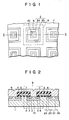
- p type base region 2 is formed in the surface region of n type silicon substrate 1.
- n type source region 3 is formed in the surface region of base region 2.
- Base region 2 comprises first region 2a, second region 2b and third region 2c.
- Gate insulating layer 4 is provided on that portion of the substrate 1 which intervenes between two adjacent base regions 2, 2.
- Gate electrode 5 is mounted on gate insulating layer 4.
- Channel region 6 is formed between the surface of first region 2a and gate insulating layer 4.
- Source region 3 is formed in second region 2b of base region 2.
- Gate insulating layer 4 and gate electrode 5 are covered with insulating layer 7.
- Common source electrode 8 is provided in contact with the surface of third region 2c of base region 2 and part of the surface of source region 3.
- a region surrounded by dotted lines constitutes unit cell 9.
- Fig. 1 indicates the pattern of the main surface of substrate 1.
- Reference numeral 2c denotes the third region contacting electrode 8.
- Reference numeral 3a represents an area of source region 3 contacting electrode 8.
- Reference numeral 3b shows the surface area of source region 3, except for area 3a.
- Reference numeral 6 shows the surface area of channel region.
- a semiconductor device illustrated in Figs. 1 and 2 is constructed as described below.
- An insulating layer is formed on substrate 1.
- a layer for forming gate electrode 5 is deposited on the insulating layer and then patterned to provide gate electrode 5 shown in Fig. 3.
- Gate electrode 5 comprises a plurality of holes 10 of Ls ⁇ Ls (Ls represents a source length).
- An interval (gate length) of respective holes 10 is denoted by character L G .
- Gate insulating layer 4 is patterned with gate electrode 5 used as a mask.
- a p type impurity is diffused through the surface of n type substrate 1 with gate electrode 5 used as a mask, thereby providing base region 2.
- n type impurity is diffused with gate electrode 5 again used as a mask, thereby forming source region 3.
- channel region 6 is formed with the effective channel length which corresponds to a difference between the depths with which base region 2 and source region 3 are diffused.
- source region 3 is formed, n type impurity is not diffused into third region 2c of the base region.
- insulating layer 7 and source electrode 8 are formed. The surface of third region 2c is brought into contact with source electrode 8. As a result, channel region 6 is grounded through base region 2.
- third region 2c of base region 2 is intended to cause base region 2 and channel region 6 to be connected to source electrode 8 and ground regions 2 and 6 through source electrode 8. While the semiconductor device of Fig. 2 remains in a normal operating condition, namely, drain current passes through source electrode 8, source region 3, channel region 6, and drain region 1, then second region 2c does not act as a current path. As viewed only from the current path, it would be possible, as naturally expected, to miniaturize the size of the gate electrode pattern shown in Fig. 3 without providing third region 2c.
- third region 2c base region 2 and channel region 6 would be electrically set in a floating condition, leading to the occurrence of a parasitic transistor effect. If, therefore, it is intended to let the subject vertical MOS semiconductor device be constructed with a high withstand voltage or be operated with a high frequency, the appearance of the above-mentioned parasitic transistor effect would be objectionable. Consequently, it would be impossible to dispense with third region 2c. If, therefore, it is desired to shorten source length L S of Fig. 3, it will be necessary to minimize the area of third region 2c. Moreover, channel region 6 fails to be reliably grounded simply by reducing the area of third region 2c.
- the object of this invention is to provide a vertical MOS semiconductor device, which is characterized in that, even when the surface area of the third region of the base region is reduced, the channel region can be reliably grounded; and the resistance to the drain current flowing through the channel region can be decreased.
- this invention provides a vertical MOS semiconductor device which comprises: a semiconductor substrate of first conductivity type; a gate insulating layer mounted on a part of the semiconductor substrate, a gate electrode being provided on the gate insulating layer; a base region of second conductivity type formed in a surface region of the semiconductor substrate and comprising first, second and third regions, a channel region being formed between the surface of the first region and the gate insulating layer, a source region of the first conductivity type being formed in the second region, and a source electrode contacting the third region.
- the base region further comprises a fourth region extending from the third region so as to divide the source region and also contact the channel region.
- a third region of the base region namely, that portion of the base region which contacts the source electrode, extends so as to divide the source region in two and contacts the channel region. If, therefore, the surface area of the third region is made smaller than in the prior art, the channel region can be reliably grounded. Further, the reduced area of the third region makes it possible to miniaturize the pattern of the gate electrode, namely, to increase the density of the assembled unit cells. This means that the total gate width (namely, the total sum of the channel widths of all the unit cells) can be extended, namely, R ON can be decreased.
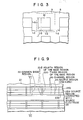
- reference numeral 20 represents a unit cell.
- a plurality of p type base regions 22 are provided in a matrix form in the surface region of an n type silicon substrate 21.
- Each base region 22 comprises first region 22a, second region 22b, and third region 22c.
- Source regions 23, 23 are formed in second region 22b.
- Gate insulating layer 24 is provided on that portion of the substrate which intervenes between two adjacent base regions 22 so as to bridge the end portions of the corresponding base regions.
- Gate electrode 25 (Fig. 7) is provided on gate insulating layer 24.
- Channel region 26 is formed between gate insulation layer 24 and first region 22a of base region 22. Insulating layer 27 covers gate electrode 25.
- Common source electrode 28 contacts third portion 22c of base region 22 and part of source region 23.
- reference numeral 23a denotes that portion of source region 23 which contacts source electrode 28.
- Reference numeral 23b represents the portion of source region 23 other than region 23a. Therefore, portions 23a and 23b jointly represent the surface area of source region 23.
- reference numeral 22c denotes the surface area of third region of base region 22 contacting source electrode 28.
- Two extensions 22d from third region 22c which run parallel to line VI-VI jointly constitute the fourth region of base region 22, and divide source region 23 in two portions and contact channel region 26. Namely, fourth region 22d causes electric contact between third region 22c and source electrode 28 to be connected directly to channel region 26.
- Substrate 21 is fabricated by growing an epitaxial layer containing phosphorus of 5.5 ⁇ 1015 cm ⁇ 3 concentration on a wafer containing antimony having a concentration of 3 ⁇ 1018.
- the epitaxial layer is positioned on the main surface of substrate 21.
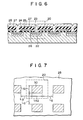
- An oxide layer is formed on the epitaxial layer with a thickness of 5000 ⁇ . Etching is applied to remove the inside portion other than the predetermined peripheral portion of the oxide layer.
- a gate oxide layer having a thickness of 1000 ⁇ and a polysilicon layer of 5000 ⁇ are deposited on the portion remaining after the etching of the 5000 ⁇ oxide layer.
- gate oxide layer 24 and gate electrode 25 are provided.
- the pattern of gate electrode 25 is as illustrated in Fig. 7.
- Gate electrode 25 is provided with a plurality of holes 30 through which an impurity is to be defused.
- boron ion is implanted at the dose rate of 3 ⁇ 1013 cm ⁇ 2 and with the acceleration voltage of 40 keV. The implanted boron ions are diffused for 3.5 hours in an N2 gas atmosphere maintained at 1100°C, thereby forming base region 22.
- ansenic ions are implanted at the dose rate of 5 ⁇ 1015 cm ⁇ 2 with the acceleration voltage of 40 KeV and annealing is applied for 20 minutes in an N2 atmosphere maintained at 1000°C, thereby providing source region 23.
- channel region 26 is formed having a channel length which corresponds to a difference between the impurity diffusion depth of base region 22 and the impurity diffusion depth of source region 23.
- a phosphorus silicate glass (PSG) layer is deposited with a thickness of 7000 ⁇ over the surface including gate electrode 25 to effect interinsulation layer 25. Contact holes are opened in those portions of the PSG layer which face aforesaid source regions 23. An aluminium layer is deposited on the PSG layer. This aluminium layer is patterned to provide source electrode 28.
- Fig. 7 represents the pattern of the electrode 25 involved in the semiconductor device of Fig. 5.
- Reference numerals L S1 , L S2 indicate source lengths
- reference numeral Lg represents a gate length.
- third region 22c of base region 22 (a contact area between base region 22 and source electrode 28) is connected to channel region 26 by means of extension 22d (fourth region) from third region 22c of base region 22. Obviously, therefore, it is possible to reduce resistance between third region 22c and channel region 26.
- the semiconductor device of Fig. 5 representing the present invention has the feature that, even if third region 22c of base region 22 contacting with electrode 28 is reduced in area, the channel region can be reliably grounded.
- the reduced area of third region 22c makes it possible to decrease the pattern size of the gate electrode, and in consequence, the magnitude of resistance R ON .
- Fig. 8 is a curve diagram showing the property of resistance R ON to gate length Lg.
- Curve 31 represents the prior art corresponding to Fig. 2.
- Curve 32 denotes the present invention of Fig. 5.
- Curves 31, 32 show that R ON changes with Lg (Figs. 3 and 7).
- Curve 32 [source lengths 9 microns (L S1 ) and 15 microns (L S2 )] indicates that R ON always has a smaller magnitude than curve 31 (source length 15 microns).
- third region 22c and extension 22d thereof extend along line VI-VI.
- these portions may be so devised as to extend along line V-V.
- the present invention is also applicable to a semiconductor device involving stripe-type cells.
- the sectional view on line VI-VI of Fig. 9 is the same as that of Fig. 6.
- two source regions 23, 23 are formed in base region 22.
- Fig. 9 indicates the device where more than two source regions 23 are provided in common base region 22.
- the parts the same as those of Fig. 5 are denoted by the same numerals, description thereof being omitted.
Abstract
Description
- This invention relates to a vertical MOS type semiconductor device.
- A vertical MOS type semiconductor device is mainly used for switching. In normal operation, a drain current runs through a source electrode, source region, channel region and drain region of the device. In this case, passage resistance to the drain current, namely, RON has to be minimized. However, the prior art semiconductor device presented difficulties in reducing RON to a satisfactory extent. Description may now be made of the construction of the conventional vertical MOS transistor with reference to Figs. 1 to 3. Referring to Figs. 1 and 2, p
type base region 2 is formed in the surface region of n type silicon substrate 1. ntype source region 3 is formed in the surface region ofbase region 2.Base region 2 comprises first region 2a, second region 2b andthird region 2c.Gate insulating layer 4 is provided on that portion of the substrate 1 which intervenes between twoadjacent base regions Gate electrode 5 is mounted ongate insulating layer 4.Channel region 6 is formed between the surface of first region 2a andgate insulating layer 4.Source region 3 is formed in second region 2b ofbase region 2.Gate insulating layer 4 andgate electrode 5 are covered withinsulating layer 7.Common source electrode 8 is provided in contact with the surface ofthird region 2c ofbase region 2 and part of the surface ofsource region 3. A region surrounded by dotted lines constitutesunit cell 9. Fig. 1 indicates the pattern of the main surface of substrate 1.Reference numeral 2c denotes the thirdregion contacting electrode 8. Reference numeral 3a represents an area ofsource region 3 contactingelectrode 8.Reference numeral 3b shows the surface area ofsource region 3, except for area 3a.Reference numeral 6 shows the surface area of channel region. - A semiconductor device illustrated in Figs. 1 and 2 is constructed as described below. An insulating layer is formed on substrate 1. A layer for forming
gate electrode 5 is deposited on the insulating layer and then patterned to providegate electrode 5 shown in Fig. 3.Gate electrode 5 comprises a plurality ofholes 10 of Ls × Ls (Ls represents a source length). An interval (gate length) ofrespective holes 10 is denoted by character LG. Gateinsulating layer 4 is patterned withgate electrode 5 used as a mask. A p type impurity is diffused through the surface of n type substrate 1 withgate electrode 5 used as a mask, thereby providingbase region 2. Later, an n type impurity is diffused withgate electrode 5 again used as a mask, thereby formingsource region 3. In this case,channel region 6 is formed with the effective channel length which corresponds to a difference between the depths with whichbase region 2 andsource region 3 are diffused. Whensource region 3 is formed, n type impurity is not diffused intothird region 2c of the base region. Later, insulatinglayer 7 andsource electrode 8 are formed. The surface ofthird region 2c is brought into contact withsource electrode 8. As a result,channel region 6 is grounded throughbase region 2. - When the MOS transistor device of Fig. 2 is rendered conductive, drain current flows through
source electrode 8,source region 3,channel region 6 and drain region 1 (substrate). When the ON resistance (hereinafter referred to as "RON") of the entire above-mentioned passage should be reduced, it is necessary to enlarge the total gate widths of all the cells. Now, let it be assumed that the gate width of each cell corresponds to, for example, the circumferential length ofchannel region 6 of Fig. 1. If, therefore, it is intended to enlarge the total sum of the channel widths of the cells, it is necessary to minimize the size of the pattern of Fig. 1. In other words, the density of the assembled unit cells has to be increased. If the pattern ofgate electrode 5 shown in Fig. 3 is reduced in size, it will be necessary to shorten the gate length LG and source length LS. Referring to Figs. 1 and 2,third region 2c ofbase region 2 is intended to causebase region 2 andchannel region 6 to be connected tosource electrode 8 andground regions source electrode 8. While the semiconductor device of Fig. 2 remains in a normal operating condition, namely, drain current passes throughsource electrode 8,source region 3,channel region 6, and drain region 1, thensecond region 2c does not act as a current path. As viewed only from the current path, it would be possible, as naturally expected, to miniaturize the size of the gate electrode pattern shown in Fig. 3 without providingthird region 2c. Unless, however,third region 2c is provided,base region 2 andchannel region 6 would be electrically set in a floating condition, leading to the occurrence of a parasitic transistor effect. If, therefore, it is intended to let the subject vertical MOS semiconductor device be constructed with a high withstand voltage or be operated with a high frequency, the appearance of the above-mentioned parasitic transistor effect would be objectionable. Consequently, it would be impossible to dispense withthird region 2c. If, therefore, it is desired to shorten source length LS of Fig. 3, it will be necessary to minimize the area ofthird region 2c. Moreover,channel region 6 fails to be reliably grounded simply by reducing the area ofthird region 2c. - The object of this invention is to provide a vertical MOS semiconductor device, which is characterized in that, even when the surface area of the third region of the base region is reduced, the channel region can be reliably grounded; and the resistance to the drain current flowing through the channel region can be decreased.
- To attain the above-mentioned object, this invention provides a vertical MOS semiconductor device which comprises: a semiconductor substrate of first conductivity type; a gate insulating layer mounted on a part of the semiconductor substrate, a gate electrode being provided on the gate insulating layer; a base region of second conductivity type formed in a surface region of the semiconductor substrate and comprising first, second and third regions, a channel region being formed between the surface of the first region and the gate insulating layer, a source region of the first conductivity type being formed in the second region, and a source electrode contacting the third region. The base region further comprises a fourth region extending from the third region so as to divide the source region and also contact the channel region.
- According to this invention, a third region of the base region, namely, that portion of the base region which contacts the source electrode, extends so as to divide the source region in two and contacts the channel region. If, therefore, the surface area of the third region is made smaller than in the prior art, the channel region can be reliably grounded. Further, the reduced area of the third region makes it possible to miniaturize the pattern of the gate electrode, namely, to increase the density of the assembled unit cells. This means that the total gate width (namely, the total sum of the channel widths of all the unit cells) can be extended, namely, RON can be decreased.
- This invention can be more fully understood from the following detailed description when taken in conjunction with the accompanying drawings, in which:
- Fig. 1 is a plan view of the main surface of the semiconductor substrate of the conventional vertical MOS type semiconductor device;
- Fig. 2 is a sectional view on line II-II of Fig. 1;
- Fig. 3 is a plan view of the gate electrode of Fig. 2;
- Fig. 4 is a plan view of the substrate of a semiconductor device according to a first embodiment of the present invention;
- Fig. 5 is a sectional view on line V-V of Fig. 4;
- Fig. 6 is a sectional view on line VI-VI of Fig. 4;
- Fig. 7 is a plan view of the gate electrode of Fig. 5;
- Fig. 8 diagramatically shows the relationship between the magnitude of RON of the semiconductor device of the present invention and that of RON of the conventional semiconductor device of Fig. 1; and
- Fig. 9 is a plan view of the main surface of a semiconductor device according to a second embodiment of the invention.
- Referring to Figs. 4 and 5,
reference numeral 20 represents a unit cell. A plurality of ptype base regions 22 are provided in a matrix form in the surface region of an ntype silicon substrate 21. Eachbase region 22 comprises first region 22a, second region 22b, and third region 22c.Source regions Gate insulating layer 24 is provided on that portion of the substrate which intervenes between twoadjacent base regions 22 so as to bridge the end portions of the corresponding base regions. Gate electrode 25 (Fig. 7) is provided ongate insulating layer 24.Channel region 26 is formed betweengate insulation layer 24 and first region 22a ofbase region 22. Insulatinglayer 27 coversgate electrode 25. Common source electrode 28 contacts third portion 22c ofbase region 22 and part ofsource region 23. Referring to Fig. 4,reference numeral 23a denotes that portion ofsource region 23 which contacts sourceelectrode 28.Reference numeral 23b represents the portion ofsource region 23 other thanregion 23a. Therefore,portions source region 23. Referring to Fig. 4, reference numeral 22c denotes the surface area of third region ofbase region 22 contactingsource electrode 28. Twoextensions 22d from third region 22c which run parallel to line VI-VI jointly constitute the fourth region ofbase region 22, and dividesource region 23 in two portions andcontact channel region 26. Namely,fourth region 22d causes electric contact between third region 22c and source electrode 28 to be connected directly tochannel region 26. - The same parts of Fig. 6 as those of Fig. 5 are denoted by the same numerals, description thereof being omitted.
- Description may now be made of the method of manufacturing a vertical MOS semiconductor device illustrated in Fig. 5.
Substrate 21 is fabricated by growing an epitaxial layer containing phosphorus of 5.5 × 10¹⁵ cm⁻³ concentration on a wafer containing antimony having a concentration of 3 × 10¹⁸. The epitaxial layer is positioned on the main surface ofsubstrate 21. An oxide layer is formed on the epitaxial layer with a thickness of 5000 Å. Etching is applied to remove the inside portion other than the predetermined peripheral portion of the oxide layer. A gate oxide layer having a thickness of 1000 Å and a polysilicon layer of 5000 Å are deposited on the portion remaining after the etching of the 5000 Å oxide layer. After subsequent etching,gate oxide layer 24 andgate electrode 25 are provided. The pattern ofgate electrode 25 is as illustrated in Fig. 7.Gate electrode 25 is provided with a plurality ofholes 30 through which an impurity is to be defused. Withgate electrode 25 of Fig. 7 used as a mask, boron ion is implanted at the dose rate of 3 ×10¹³ cm⁻² and with the acceleration voltage of 40 keV. The implanted boron ions are diffused for 3.5 hours in an N₂ gas atmosphere maintained at 1100°C, thereby formingbase region 22. Later, with the aid of a resist mask, ansenic ions are implanted at the dose rate of 5 ×10¹⁵ cm⁻² with the acceleration voltage of 40 KeV and annealing is applied for 20 minutes in an N₂ atmosphere maintained at 1000°C, thereby providingsource region 23. At this time,channel region 26 is formed having a channel length which corresponds to a difference between the impurity diffusion depth ofbase region 22 and the impurity diffusion depth ofsource region 23. Whensource region 23 is provided,regions 22c and 22d shown in Fig. 4 are retained thereby to effect a direct connection betweensource electrode 28 andchannel region 26. Later, a phosphorus silicate glass (PSG) layer is deposited with a thickness of 7000 Å over the surface includinggate electrode 25 to effectinterinsulation layer 25. Contact holes are opened in those portions of the PSG layer which faceaforesaid source regions 23. An aluminium layer is deposited on the PSG layer. This aluminium layer is patterned to providesource electrode 28. Fig. 7 represents the pattern of theelectrode 25 involved in the semiconductor device of Fig. 5. Reference numerals LS1, LS2 indicate source lengths, and reference numeral Lg represents a gate length. - As seen from Figs. 4 and 5, third region 22c of base region 22 (a contact area between
base region 22 and source electrode 28) is connected to channelregion 26 by means ofextension 22d (fourth region) from third region 22c ofbase region 22. Obviously, therefore, it is possible to reduce resistance between third region 22c andchannel region 26. Unlike the conventional semiconductor device, the semiconductor device of Fig. 5 representing the present invention has the feature that, even if third region 22c ofbase region 22 contacting withelectrode 28 is reduced in area, the channel region can be reliably grounded. The reduced area of third region 22c makes it possible to decrease the pattern size of the gate electrode, and in consequence, the magnitude of resistance RON. - Fig. 8 is a curve diagram showing the property of resistance RON to gate length Lg. Curve 31 represents the prior art corresponding to Fig. 2. Curve 32 denotes the present invention of Fig. 5. Curves 31, 32 show that RON changes with Lg (Figs. 3 and 7). Curve 32 [
source lengths 9 microns (LS1) and 15 microns (LS2)] indicates that RON always has a smaller magnitude than curve 31 (source length 15 microns). - It should be noted that the present invention is not limited to the aforementioned embodiment. Referring to Fig. 4, third region 22c and
extension 22d thereof (fourth portion) extend along line VI-VI. However, these portions may be so devised as to extend along line V-V. The present invention is also applicable to a semiconductor device involving stripe-type cells. The sectional view on line VI-VI of Fig. 9 is the same as that of Fig. 6. In Fig. 5, twosource regions base region 22. In contrast, Fig. 9 indicates the device where more than twosource regions 23 are provided incommon base region 22. The parts the same as those of Fig. 5 are denoted by the same numerals, description thereof being omitted.
Claims (3)
a semiconductor substrate (21) of first conductivity type;
a gate insulating layer (24) mounted on a part of said semiconductor substrate, a gate electrode (25) being provided on said gate insulating layer;
a base region (22) of second conductivity type formed in a surface region of said semiconductor substrate and comprising first, second and third regions (22a, 22b, 22c), a channel region (26) being formed between the surface of said first region (22a) and said gate insulating layer, a source region (23) of said first conductivity type being formed in said second region (22b), and a source electrode (28) contacting said third region (22c);
characterized in that said base region (22) further comprises a fourth region (22d) extending from said third region (22c) so as to divide said source region and also contact said channel region (26).
Applications Claiming Priority (2)
| Application Number | Priority Date | Filing Date | Title |
|---|---|---|---|
| JP161601/86 | 1986-07-09 | ||
| JP61161601A JPH07120794B2 (en) | 1986-07-09 | 1986-07-09 | MOS semiconductor device |
Publications (2)
| Publication Number | Publication Date |
|---|---|
| EP0252236A2 true EP0252236A2 (en) | 1988-01-13 |
| EP0252236A3 EP0252236A3 (en) | 1990-01-31 |
Family
ID=15738254
Family Applications (1)
| Application Number | Title | Priority Date | Filing Date |
|---|---|---|---|
| EP87106481A Ceased EP0252236A3 (en) | 1986-07-09 | 1987-05-05 | Vertical mos type semiconductor device |
Country Status (3)
| Country | Link |
|---|---|
| EP (1) | EP0252236A3 (en) |
| JP (1) | JPH07120794B2 (en) |
| KR (1) | KR900007048B1 (en) |
Cited By (12)
| Publication number | Priority date | Publication date | Assignee | Title |
|---|---|---|---|---|
| EP0661755A1 (en) * | 1993-12-28 | 1995-07-05 | AT&T Corp. | High voltage semiconductor device having improved electrical ruggedness and reduced cell pitch |
| EP0772241A1 (en) * | 1995-10-30 | 1997-05-07 | STMicroelectronics S.r.l. | High density MOS technology power device |
| EP0772242A1 (en) * | 1995-10-30 | 1997-05-07 | STMicroelectronics S.r.l. | Single feature size MOS technology power device |
| EP0848430A2 (en) * | 1996-12-12 | 1998-06-17 | Westinghouse Brake And Signal Holdings Limited | Insulated gate bipolar transistor |
| US5798554A (en) * | 1995-02-24 | 1998-08-25 | Consorzio Per La Ricerca Sulla Microelettronica Nel Mezzogiorno | MOS-technology power device integrated structure and manufacturing process thereof |
| US5841167A (en) * | 1995-12-28 | 1998-11-24 | Sgs-Thomson Microelectronics S.R.L. | MOS-technology power device integrated structure |
| EP0892435A1 (en) * | 1997-07-14 | 1999-01-20 | STMicroelectronics S.r.l. | Integrated semiconductor transistor with current sensing |
| US5900662A (en) * | 1995-11-06 | 1999-05-04 | Sgs Thomson Microelectronics S.R.L. | MOS technology power device with low output resistance and low capacitance, and related manufacturing process |
| US6090669A (en) * | 1995-10-09 | 2000-07-18 | Consorzio Per La Ricerca Sulla Microelectronics Nel Mezzogiorno | Fabrication method for high voltage devices with at least one deep edge ring |
| US6228719B1 (en) | 1995-11-06 | 2001-05-08 | Stmicroelectronics S.R.L. | MOS technology power device with low output resistance and low capacitance, and related manufacturing process |
| US6492691B2 (en) | 1998-05-26 | 2002-12-10 | Stmicroelectronics S.R.L. | High integration density MOS technology power device structure |
| US10856963B2 (en) | 2017-04-11 | 2020-12-08 | Hangzhou Wei Qiang Medical Technology Co., Ltd. | Inferior vena cava filter of bidirectional controlled placement |
Citations (3)
| Publication number | Priority date | Publication date | Assignee | Title |
|---|---|---|---|---|
| JPS5889864A (en) * | 1981-11-24 | 1983-05-28 | Hitachi Ltd | Insulated gate type semiconductor device |
| EP0091079A2 (en) * | 1982-04-01 | 1983-10-12 | Kabushiki Kaisha Toshiba | Power MOSFET |
| US4639762A (en) * | 1984-04-30 | 1987-01-27 | Rca Corporation | MOSFET with reduced bipolar effects |
Family Cites Families (2)
| Publication number | Priority date | Publication date | Assignee | Title |
|---|---|---|---|---|
| US4345265A (en) * | 1980-04-14 | 1982-08-17 | Supertex, Inc. | MOS Power transistor with improved high-voltage capability |
| US4809045A (en) * | 1985-09-30 | 1989-02-28 | General Electric Company | Insulated gate device |
-
1986
- 1986-07-09 JP JP61161601A patent/JPH07120794B2/en not_active Expired - Lifetime
-
1987
- 1987-05-05 EP EP87106481A patent/EP0252236A3/en not_active Ceased
- 1987-07-09 KR KR1019870007366A patent/KR900007048B1/en not_active IP Right Cessation
Patent Citations (3)
| Publication number | Priority date | Publication date | Assignee | Title |
|---|---|---|---|---|
| JPS5889864A (en) * | 1981-11-24 | 1983-05-28 | Hitachi Ltd | Insulated gate type semiconductor device |
| EP0091079A2 (en) * | 1982-04-01 | 1983-10-12 | Kabushiki Kaisha Toshiba | Power MOSFET |
| US4639762A (en) * | 1984-04-30 | 1987-01-27 | Rca Corporation | MOSFET with reduced bipolar effects |
Non-Patent Citations (2)
| Title |
|---|
| IEEE ELECTRON DEVICE LETTERS, vol. EDL-6, no. 8, August 1985, pages 419-421, New York, USA; H. YILMAZ: "Cell Geometry Effect on IGT Latch-Up". * |
| PATENT ABSTRACTS OF JAPAN, vol. 7, no. 186 (E-193)(1331) 16 August 1983; & JP-A-58 089 864 (HITACHI SEISAKUSHO K.K.) 28-05-1983 * |
Cited By (27)
| Publication number | Priority date | Publication date | Assignee | Title |
|---|---|---|---|---|
| US5541429A (en) * | 1993-12-28 | 1996-07-30 | At&T Corp. | High voltage semiconductor device having improved electrical ruggedness and reduced cell pitch |
| EP0661755A1 (en) * | 1993-12-28 | 1995-07-05 | AT&T Corp. | High voltage semiconductor device having improved electrical ruggedness and reduced cell pitch |
| US5798554A (en) * | 1995-02-24 | 1998-08-25 | Consorzio Per La Ricerca Sulla Microelettronica Nel Mezzogiorno | MOS-technology power device integrated structure and manufacturing process thereof |
| US6111297A (en) * | 1995-02-24 | 2000-08-29 | Consorzio Per La Ricerca Sulla Microelettronica Nel Mezzogiorno | MOS-technology power device integrated structure and manufacturing process thereof |
| US6090669A (en) * | 1995-10-09 | 2000-07-18 | Consorzio Per La Ricerca Sulla Microelectronics Nel Mezzogiorno | Fabrication method for high voltage devices with at least one deep edge ring |
| US5985721A (en) * | 1995-10-30 | 1999-11-16 | Sgs-Thomson Microelectronics, S.R.L. | Single feature size MOS technology power device |
| US6064087A (en) * | 1995-10-30 | 2000-05-16 | Sgs-Thomson Microelectronics, S.R.L. | Single feature size MOS technology power device |
| US6566690B2 (en) | 1995-10-30 | 2003-05-20 | Sgs Thomson Microelectronics S.R.L. | Single feature size MOS technology power device |
| US6548864B2 (en) | 1995-10-30 | 2003-04-15 | Sgs Thomson Microelectronics | High density MOS technology power device |
| US6468866B2 (en) | 1995-10-30 | 2002-10-22 | Sgs-Thomson Microelectronics S.R.L. | Single feature size MOS technology power device |
| US5981998A (en) * | 1995-10-30 | 1999-11-09 | Sgs-Thomson Microelectronics S.R.L. | Single feature size MOS technology power device |
| US5981343A (en) * | 1995-10-30 | 1999-11-09 | Sgs-Thomas Microelectronics, S.R.L. | Single feature size mos technology power device |
| EP0772241A1 (en) * | 1995-10-30 | 1997-05-07 | STMicroelectronics S.r.l. | High density MOS technology power device |
| US6030870A (en) * | 1995-10-30 | 2000-02-29 | Sgs-Thomson Microelectronics, S.R.L. | High density MOS technology power device |
| EP0772242A1 (en) * | 1995-10-30 | 1997-05-07 | STMicroelectronics S.r.l. | Single feature size MOS technology power device |
| US6054737A (en) * | 1995-10-30 | 2000-04-25 | Sgs-Thomson Microelectronics S.R.L. | High density MOS technology power device |
| US6228719B1 (en) | 1995-11-06 | 2001-05-08 | Stmicroelectronics S.R.L. | MOS technology power device with low output resistance and low capacitance, and related manufacturing process |
| US5900662A (en) * | 1995-11-06 | 1999-05-04 | Sgs Thomson Microelectronics S.R.L. | MOS technology power device with low output resistance and low capacitance, and related manufacturing process |
| US5841167A (en) * | 1995-12-28 | 1998-11-24 | Sgs-Thomson Microelectronics S.R.L. | MOS-technology power device integrated structure |
| US6051862A (en) * | 1995-12-28 | 2000-04-18 | Sgs-Thomson Microelectronics S.R.L. | MOS-technology power device integrated structure |
| EP0848430A2 (en) * | 1996-12-12 | 1998-06-17 | Westinghouse Brake And Signal Holdings Limited | Insulated gate bipolar transistor |
| US6147382A (en) * | 1996-12-12 | 2000-11-14 | Westcode Semiconductors Limited | Semiconductor switching device with segmented sources |
| EP0848430A3 (en) * | 1996-12-12 | 1999-01-13 | Westinghouse Brake And Signal Holdings Limited | Insulated gate bipolar transistor |
| US6140680A (en) * | 1997-07-14 | 2000-10-31 | Thomson Microelectronics, S.R.L. | Integrated power semiconductor transistor with current sensing |
| EP0892435A1 (en) * | 1997-07-14 | 1999-01-20 | STMicroelectronics S.r.l. | Integrated semiconductor transistor with current sensing |
| US6492691B2 (en) | 1998-05-26 | 2002-12-10 | Stmicroelectronics S.R.L. | High integration density MOS technology power device structure |
| US10856963B2 (en) | 2017-04-11 | 2020-12-08 | Hangzhou Wei Qiang Medical Technology Co., Ltd. | Inferior vena cava filter of bidirectional controlled placement |
Also Published As
| Publication number | Publication date |
|---|---|
| KR900007048B1 (en) | 1990-09-27 |
| KR880002275A (en) | 1988-04-30 |
| JPH07120794B2 (en) | 1995-12-20 |
| JPS6317560A (en) | 1988-01-25 |
| EP0252236A3 (en) | 1990-01-31 |
Similar Documents
| Publication | Publication Date | Title |
|---|---|---|
| EP0772242B1 (en) | Single feature size MOS technology power device | |
| EP0620588B1 (en) | A method of manufacturing a recessed insulated gate field-effect semiconductor device | |
| JP3844535B2 (en) | Power MOSFET edge termination method and structure | |
| US6673680B2 (en) | Field coupled power MOSFET bus architecture using trench technology | |
| EP0241059A2 (en) | Method for manufacturing a power mos transistor | |
| JPH07122745A (en) | Semiconductor device and its manufacture | |
| JP2002110978A (en) | Power semiconductor element | |
| JP2004528719A (en) | Double diffused metal oxide semiconductor transistor with zener diode for electrostatic discharge protection | |
| JPS60253275A (en) | High density v-groove mos control thyristor, insulated gate type transistor and mosfet as well as method of producing same | |
| EP0252236A2 (en) | Vertical MOS type semiconductor device | |
| US3883372A (en) | Method of making a planar graded channel MOS transistor | |
| EP0772241A1 (en) | High density MOS technology power device | |
| US6635535B2 (en) | Dense trench MOSFET with decreased etch sensitivity to deposition and etch processing | |
| US4816882A (en) | Power MOS transistor with equipotential ring | |
| JP2002016080A (en) | Manufacturing method of trench-gate type mosfet | |
| KR19990050418A (en) | Power Device with Double Field Plate Structure | |
| JPH0521793A (en) | Semiconductor device and fabrication thereof | |
| JP3354127B2 (en) | High voltage element and method of manufacturing the same | |
| EP0159179A2 (en) | Improved bipolar transistor construction | |
| JPH08125180A (en) | Semiconductor device and fabrication thereof | |
| JPH08213638A (en) | Mosfet on soi substrate and its manufacture | |
| JP2881267B2 (en) | Semiconductor device and manufacturing method thereof | |
| US6893923B2 (en) | Reduced mask count process for manufacture of mosgated device | |
| CN101442008B (en) | Insulated gate semiconductor device and novel self-alignment manufacture method thereof | |
| JPH0363210B2 (en) |
Legal Events
| Date | Code | Title | Description |
|---|---|---|---|
| PUAI | Public reference made under article 153(3) epc to a published international application that has entered the european phase |
Free format text: ORIGINAL CODE: 0009012 |
|
| 17P | Request for examination filed |
Effective date: 19870505 |
|
| AK | Designated contracting states |
Kind code of ref document: A2 Designated state(s): DE FR GB |
|
| PUAL | Search report despatched |
Free format text: ORIGINAL CODE: 0009013 |
|
| AK | Designated contracting states |
Kind code of ref document: A3 Designated state(s): DE FR GB |
|
| 17Q | First examination report despatched |
Effective date: 19910823 |
|
| STAA | Information on the status of an ep patent application or granted ep patent |
Free format text: STATUS: THE APPLICATION HAS BEEN REFUSED |
|
| 18R | Application refused |
Effective date: 19941201 |
|
| RIN1 | Information on inventor provided before grant (corrected) |
Inventor name: MATSUNAGA, TAIRAPATENT DIVISION Inventor name: ISHII, TETSUOPATENT DIVISION Inventor name: KIMURA, TAKASHIPATENT DIVISION |