EP0251276A2 - A recording/reproducing system for a magnetic recording medium - Google Patents
A recording/reproducing system for a magnetic recording medium Download PDFInfo
- Publication number
- EP0251276A2 EP0251276A2 EP87109330A EP87109330A EP0251276A2 EP 0251276 A2 EP0251276 A2 EP 0251276A2 EP 87109330 A EP87109330 A EP 87109330A EP 87109330 A EP87109330 A EP 87109330A EP 0251276 A2 EP0251276 A2 EP 0251276A2
- Authority
- EP
- European Patent Office
- Prior art keywords
- data
- signal
- head
- recording medium
- magnetic
- Prior art date
- Legal status (The legal status is an assumption and is not a legal conclusion. Google has not performed a legal analysis and makes no representation as to the accuracy of the status listed.)
- Granted
Links
Images


Classifications
-
- G—PHYSICS
- G11—INFORMATION STORAGE
- G11B—INFORMATION STORAGE BASED ON RELATIVE MOVEMENT BETWEEN RECORD CARRIER AND TRANSDUCER
- G11B5/00—Recording by magnetisation or demagnetisation of a record carrier; Reproducing by magnetic means; Record carriers therefor
- G11B5/02—Recording, reproducing, or erasing methods; Read, write or erase circuits therefor
-
- G—PHYSICS
- G11—INFORMATION STORAGE
- G11B—INFORMATION STORAGE BASED ON RELATIVE MOVEMENT BETWEEN RECORD CARRIER AND TRANSDUCER
- G11B20/00—Signal processing not specific to the method of recording or reproducing; Circuits therefor
- G11B20/10—Digital recording or reproducing
- G11B20/10009—Improvement or modification of read or write signals
- G11B20/10018—Improvement or modification of read or write signals analog processing for digital recording or reproduction
- G11B20/10027—Improvement or modification of read or write signals analog processing for digital recording or reproduction adjusting the signal strength during recording or reproduction, e.g. variable gain amplifiers
-
- G—PHYSICS
- G06—COMPUTING; CALCULATING OR COUNTING
- G06K—GRAPHICAL DATA READING; PRESENTATION OF DATA; RECORD CARRIERS; HANDLING RECORD CARRIERS
- G06K1/00—Methods or arrangements for marking the record carrier in digital fashion
-
- G—PHYSICS
- G11—INFORMATION STORAGE
- G11B—INFORMATION STORAGE BASED ON RELATIVE MOVEMENT BETWEEN RECORD CARRIER AND TRANSDUCER
- G11B20/00—Signal processing not specific to the method of recording or reproducing; Circuits therefor
- G11B20/10—Digital recording or reproducing
- G11B20/10009—Improvement or modification of read or write signals
- G11B20/10222—Improvement or modification of read or write signals clock-related aspects, e.g. phase or frequency adjustment or bit synchronisation
-
- G—PHYSICS
- G11—INFORMATION STORAGE
- G11B—INFORMATION STORAGE BASED ON RELATIVE MOVEMENT BETWEEN RECORD CARRIER AND TRANSDUCER
- G11B20/00—Signal processing not specific to the method of recording or reproducing; Circuits therefor
- G11B20/10—Digital recording or reproducing
- G11B20/14—Digital recording or reproducing using self-clocking codes
- G11B20/1403—Digital recording or reproducing using self-clocking codes characterised by the use of two levels
-
- G—PHYSICS
- G11—INFORMATION STORAGE
- G11B—INFORMATION STORAGE BASED ON RELATIVE MOVEMENT BETWEEN RECORD CARRIER AND TRANSDUCER
- G11B5/00—Recording by magnetisation or demagnetisation of a record carrier; Reproducing by magnetic means; Record carriers therefor
- G11B5/012—Recording on, or reproducing or erasing from, magnetic disks
-
- G—PHYSICS
- G11—INFORMATION STORAGE
- G11B—INFORMATION STORAGE BASED ON RELATIVE MOVEMENT BETWEEN RECORD CARRIER AND TRANSDUCER
- G11B5/00—Recording by magnetisation or demagnetisation of a record carrier; Reproducing by magnetic means; Record carriers therefor
- G11B5/02—Recording, reproducing, or erasing methods; Read, write or erase circuits therefor
- G11B5/09—Digital recording
Definitions
- This invention relates to a recording/reproducing system used in conjunction with a magnetic disk apparatus which reproduces data.
- a preceding-erase type magnetic head In the field of floppy disk apparatuses, a preceding-erase type magnetic head has recently been devised which is suitable for use with a high-density magnetic recording medium (disk).
- an erase head In the preceding-erase type magnetic head, an erase head is located in front of a read/write head in the rotational direction of the medium. Before new data are recorded in the medium by the read/write head, previously-recorded data are first erased by the erase head.
- the erase head should preferably be turned on at a predetermined time before the recording of data on the medium, by the read/write head, begins, and turned off at a predetermined time before the recording of data ends.
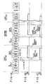
- a track has a format shown in Fig. 1A, i.e. in which one sector comprises an ID field and a data field.
- the ID field comprises a synchronization area SYNC, an address mark area AM, an identification area ID, and a cyclic redundancy check area CRC. Information representative of the starting position and address of a sector are recorded in the ID field.
- the data field stores data, and comprises synchronization area SYNC, address mark area AM, data area DATA, and cyclic redundancy check area CRC.
- Synchronization areas SYNC of the ID field and the data field store synchronization data for a PLL circuit; address mark areas AM store address mark data indicative of the starting position of the ID field or the data field; ID area ID stores data such as the cylinder number, the side number, the sector number, and the length of the data field; data area DATA stores data read out or written in by a user; and cyclic redundancy check areas CRC store data for checking whether or not the data read out from the ID field or from data field contains an error.
- Gaps 1, 2, 3, and 4 are areas for absorbing a fluctuation of rotation and an error in a mechanical alignment.
- Read data reproduced from the recording medium by the magnetic head are supplied to a data separator which includes a PLL circuit and an external synchronization detecting circuit.
- the external synchronization detector detects the synchronization data in the read data, and upon detection of the synchronization data, the PLL circuit begins oscillating in synchronism with the read data and outputs data pulses and clock pulses.
- an internal synchronization detector detects the synchronization data, on the basis of the data pulse and the clock pulse, and a floppy disk controller checks whether or not the following data, other than synchronization data, are address mark data.
- the floppy disk controller When the address mark data are detected, the floppy disk controller reads out the data stored in the ID area ID or in data area DATA, on the basis of the data pulses and clock pulses. When data other than the address mark data are detected, the floppy disk controller stops operating for a predetermined time period, and then repeats the above-mentioned operation.
- Figs. 1B and 1C show the positions where the erase head and read/write head of the preceding-erase type magnetic head are turned on and off, during data are written in the medium. As is shown in Figs. 1A to 1C, DC erased areas are formed in Gap 3, where data are erased by the erase head and new data are not recorded.
- the external synchronization detection circuit when data identical to the synchronization data are recorded in the data areas, a problem arises in that the external synchronization detection circuit sometimes erroneously detects the synchronization area of the recording medium, with the result that the system may fail to read out the data from the data area.
- the external synchronization detection circuit detects the zero pattern data as the synchronization data. In this case, the PLL circuit begins the synchronization operation.
- the internal synchronization detection circuit cannot detect the synchronization data, with the result that the PLL circuit continues to perform the synchronization operation.
- the PLL circuit oscillates at a frequency greatly different from the frequency of normal read data, due to irregular pulses derived from the DC erased area. Consequently, there is the possibility that the PLL circuit will be unable to read out even the normal data.
- An object of the present invention is to provide a high reliability recording/reproducing system using a preceding-erase type magnetic head.
- a recording/reproducing system which comprises: a magnetic head of preceding-erase type, in contact with a flexible magnetic recording medium, for recording data on said magnetic recording medium and reading out data stored in said recording medium, said magnetic head having a read/write head for writing data on, and reading data from, said magnetic recording medium, and an erase head arranged in front of said read/write head for erasing data recorded on said magnetic recording medium; write means for turning said read/write head and said erase head on substantially simultaneously and for supplying a specified signal to said read/write head, to erase data recorded on said magnetic recording medium, and to write data on said magnetic recording medium; analog signal-outputting means for outputting an analog signal corresponding to the data read out by said read/write head from said magnetic recording medium; converting means for converting the analog signal to a digital signal and outputting the digital signal; PLL (Phase Locked Loop) circuit means for receiving the digital signal, and for oscillating in synchronism with the digital signal, thereby to output data
- PLL Phase Locke
- the digital signal (RD) which is reproduced from the DC erased areas in the tracks (such as GAP3) is not output.
- the data recorded in the magnetic recording medium (21) can be reliably read out.
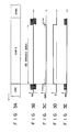
- FIG. 2 is a block diagram illustrating a first embodiment of this invention.
- magnetic head 20 is a magnetic head of the preceding-erase type, which has erase head 20A, read/write head 20B and separator 20C. Separator 20C magnetically separates erase head 20A from read/write head 20B. Erase head 20A is located in front of read/write head 20B with respect to the rotational direction of the medium 21.
- FDC 33 receives write data WD from a host computer (not shown), and supplies write data WD to write circuit 47. FDC 33 also supplies gate signal GS to write circuit 47 and selector 46. Gate signal GS functions as write gate signal WG, erase gate signal EG and select signal SS. Write gate signal WG and erase gate signal EG are supplied to write circuit 47. Select signal SS is supplied to selector 46. Selector 46 supplies write signal WS to read/write head 20B when select signal SS is H level. Selector 46 supplies output signal of read/write head 20B to preamplifier 22 when select signal SS is L level.
- the output signal of head 20 is supplied to preamplifier 22.
- Pre-amplifier 22 amplifies the output signal of magnetic head 20.
- the output signal of pre-amplifier 22 is supplied to AGC (automatic gain controlled) amplifier 24 via low-pass filter 23.
- Low-pass filter 23 removes the high-frequency noise of the output signal of pre-amplifier 22.
- AGC amplifier 24 keeps constant the amplitude of the output signal, and has a control terminal for gain adjustment.
- Output signal SA of AGC amplifier 24 is supplied to differential amplifier 25. Differential amplifier 25 detects peaks of output signal SA of AGC amplifier 24.
- the output signal of differential amplifier 25 is supplied to zero cross comparator 26.
- Zero cross comparator 26 outputs a pulse whose polarity is inverted at each zero cross point of output signal of differential amplifier 25, that is, each peak of the output signal SA of AGC amplifier 24.
- the output signal of zero cross comparator 26 is supplied to time domain filter 27.
- Time domain filter 27 removes pulses at abnormal intervals (erroneous pulses) caused by external noises and the like contained in the pulse signal from zero cross comparator 26. Filter 27 then outputs the pulse of normal intervals as the read data pulse.
- the output signal of time domain filter 27 is input to interface driver 30.
- Output signal SA of AGC amplifier 24 is also supplied to envelope detection circuit 28.
- Envelope detection circuit 28 detects signal SA to obtain the envelope of signal SA.
- Envelope detection circuit 28 outputs detect result SEN (a signal which corresponds to the detected envelope) to the terminal for gain adjustment of AGC amplifier 24. According to the signal level of signal SEN, the gain of AGC circuit 24 is controlled, so that an output signal of a constant amplitude is obtained.
- the output signal SEN of envelope detection circuit 28 is also supplied to the inverting input terminal of comparator 29.
- the reference voltage Vr is supplied to the non-inverting input terminal of comparator 29. Comparator 29 supplies signal E to the control terminal of interface driver 30.
- Signal E is high in level when the output voltage of envelope detection circuit 28 is below the reference voltage Vr.
- interface driver 30 is in an operable state, and supplies the output signal of time domain filter 27 to magnetic record/reproduction system 31 as read data RD.
- PLL circuit 32 internally includes a voltage controlled oscillator (not shown). PLL circuit 32 operates so that the phase of the output pulses are equal to that of the input pulses. PLL circuit 32 oscillates in synchronism with read data RD. It then separates read data RD into data pulses DP and clock pulses CP. Data pulses DP is a pulse signal which represents the data recorded on the tracks of magnetic recording medium 21. Clock pulses CP is a pulse signal which represents the timing for reading the data.
- FDC 33 is connected to a host computer (not shown), for example. In response to the command of the host computer, FDD 30 performs the data read-out on the basis of data pulses DP and clock pulses CP.
- the host computer supplies a write command to FDC 33.
- FDC 33 causes gate signal GS to rise to H level.
- Gate signal GS functions as write gate signal WG, erase gate signal EG and select signal SS.
- Write circuit 47 receives signals WG and EG. When write gate signal WG and erase signal EG rise to H level, write circuit 47 generates write signal WS and erase signal ES on the bases of write data WD supplied from hose computer via FDC 33 to write circuit 47.
- Write circuit 47 supplies write signal WS to selector 46, and erase signal ES to erase head 20B.
- select signal SS rises to H level, selector 46 supplied write signal WS, which has been supplied from write circuit, to read/write head 20A.
- the data recorded on medium 21 is erased by erase head 20B, and new data is recorded on medium 21 by the read/write head 20A.
- FDC 33 causes gate signal GS fall to L level.
- gate signal GS falls to L level
- write circuit 47 stops generating erase signal ES and write signal WS.
- write signal WS is not supplied to read/write head 20A
- read/write head 20A reads the data recorded on medium 21, and outputs a signal corresponding to this data.
- selector 46 supplies the output signal of read/write head 20A to preamplifier 22.
- Each track of magnetic recording medium 21 also has a format shown in Fig. 1A.
- the on/off timings of the erase head and the read/write head when the data is recorded, are same as Figs. 1B and 1C.
- the output signal of magnetic head 20 is supplied to AGC amplifier 24 via pre-amplifier 22 and low-pass filter 23.
- AGC amplifier 24 outputs signal SA of a constant amplitude, as shown in Fig. 3B.
- the output signal of AGC amplifier 24 is differentiated by differential amplifier 25.
- the differential signal is input to zero cross comparator 26.
- Differential output signal SA of AGC amplifier 24 is converted into a pulse signal by zero cross comparator 26.
- the pulse signal is input to interface driver 30 as read data pulse signal, after its abnormal pulses are removed by time domain filter 27.
- Envelope detection circuit 28 detects the envelope of output signal SA of AGC amplifier 24, and output signal SEN (which corresponds to the envelope), as shown in Fig. 3C. On the basis of the signal level of signal SEN, the amplification of AGC amplifier 24 changes, so that output signal SA of a consant amplitude is obtained.
- Comparator 29 receives signal SEN, and outputs low-level signal E, because the voltage level of signal SEN is larger than the reference voltage Vr (Fig. 3D). Vr is set to such a level that, in the normal state, the voltage level of signal SEN is larger than the reference voltage.
- interface driver 30 supplies the read data pulse from time domain filter 27 to magnetic record/reproduction system 31.
- the PLL circuit 32 of magnetic record/reproduction system 31 oscillates in synchronism with read data RD, and separates read data RD into data pulse DP and clock pulse CP.
- FDC 33 performs the data read-out.
- the amplitude of the output signal of pre-amplifier 22 is substantially zero.
- the amplitude of output signal SA of AGC amplifier 24 is also substantially zero, as shown in Fig. 3B.
- the output of time domain filter 27 is instable.
- Signal SEN is at zero level, which is below the reference voltage level Vr, as shown in Fig. 3C.
- Comparator 29 outputs high-level signal E.
- interface driver 30 Upon receipt of low-level signal E, interface driver 30 is in a high output impedance state, and does not input read data RD.
- PLL circuit 32 oscillates, while keeping the oscillating frequency up to this point.
- AGC amplifier 24 When magnetic head 20 moves out of the DC erased area, and reads the data recorded area (SYNC), again, AGC amplifier 24 outputs signal SA of a predetermined amplitude, as shown in Fig. 3B. Signal SEN exceeds the reference voltage level Vr, and the output signal of comparator 29 becomes low in level. Interface driver 30 transfers the read data pulse from time domain filter 27 to record/reproduction circuit 31 (Fig. 3E).
- read data RD is not output from interface driver 30.
- Fig. 4 FDP The structural features of the Fig. 4 FDP, as compared with the Fig. 2 FDP, are: (1) Selector 41 is provided instead of interface driver 30; (2) Oscillator 42 and frequency divider 43 are additionally used; (3) Buffer 44 is additionally used; and (4) The polarities of the input terminal of comparator 29 are opposite to those of the comparator 29 in the first embodiment.
- Selector 41 receives the output of time domain filter 27 at input terminal A, and the output signal of frequency divider 43, at input terminal B.
- Selector 41 receives the output signal E of comparator 29 at the select control terminal SEL.
- separator 29 selects read data pulse RP from time domain filter 27, and outputs the pulse RP to buffer 44.
- selector 41 selects the clock signal from frequency divider 43, and outputs the clock signal to buffer 44.
- a system clock generating circuit used in the controller of a floppy disk apparatus may be used, for example.
- Frequency divider 44 frequency divides the clock signal from oscillator 42, and outputs a clock at a frequency corresponding to the transfer rate of the normal read data RD.
- FIG. 5A When magnetic head 20 reads the not DC erased area in the tracks, AGC amplifier 24 outputs signal SA of a predetermined amplitude (Fig. 5B). Signal SEN is in level above the reference level Vr (Fig. 5C), and output signal E of comparator 29 is high in level.
- selector 41 Upon receipt of high-level signal E, selector 41 selects the output signal RP of time domain filter 27 (Fig. 5E) and outputs signal RD. Output data RD of selector 41 is supplied to magnetic record/reproduction system 31 via buffer 44.
- the clock SD from frequency divider 43 is a pulse signal at a frequency corresponding to the transfer rate of the normal read data RD.
- PLL circuit 32 in the data separator oscillates in synchronism with the input data, in the same manner as when normal read data RD is supplied.
- the read data reproduced from the DC erased areas of the magnetic recording medium is prevented from being supplied to the magnetic record/reproduction system.
- the read data with a high reliability can be obtained.
- Circuit configuration of this invention is not limited to those of Figs. 2 and 4. Other circuit configuration can be selected.
- FDC 33 may be provided in a magnetic disk apparatus or outside of the apparatus.
- Present invention can be applied to FDP having a tunnel erase head, a straddle erase head, and so on. So, data can be correctly reproduced from a medium, on which the data has been written by the preceding-erase type magnetic head, by the FDP having the tunnel erase head or the straddle erase head.
Abstract
Description
- This invention relates to a recording/reproducing system used in conjunction with a magnetic disk apparatus which reproduces data.
- In the field of floppy disk apparatuses, a preceding-erase type magnetic head has recently been devised which is suitable for use with a high-density magnetic recording medium (disk). In the preceding-erase type magnetic head, an erase head is located in front of a read/write head in the rotational direction of the medium. Before new data are recorded in the medium by the read/write head, previously-recorded data are first erased by the erase head. When this type of magnetic head is employed, the erase head should preferably be turned on at a predetermined time before the recording of data on the medium, by the read/write head, begins, and turned off at a predetermined time before the recording of data ends. However, to be able to perform such a control procedure requires a controller, for turning the heads on and off, which is complicated in its construction. The conventional controller is incapable of performing such a control procedure, and for this reason, the erase head and the read/write head are turned on or off simultaneously.
- Normally, a track has a format shown in Fig. 1A, i.e. in which one sector comprises an ID field and a data field.
- The ID field comprises a synchronization area SYNC, an address mark area AM, an identification area ID, and a cyclic redundancy check area CRC. Information representative of the starting position and address of a sector are recorded in the ID field.
- The data field stores data, and comprises synchronization area SYNC, address mark area AM, data area DATA, and cyclic redundancy check area CRC.
- Synchronization areas SYNC of the ID field and the data field store synchronization data for a PLL circuit;
address mark areas AM store address mark data indicative of the starting position of the ID field or the data field;
ID area ID stores data such as the cylinder number, the side number, the sector number, and the length of the data field;
data area DATA stores data read out or written in by a user; and
cyclic redundancy check areas CRC store data for checking whether or not the data read out from the ID field or from data field contains an error. -
Gaps - Read data reproduced from the recording medium by the magnetic head are supplied to a data separator which includes a PLL circuit and an external synchronization detecting circuit.
- The external synchronization detector detects the synchronization data in the read data, and upon detection of the synchronization data, the PLL circuit begins oscillating in synchronism with the read data and outputs data pulses and clock pulses.
- When the PLL circuit operates in synchronism with the read data, an internal synchronization detector detects the synchronization data, on the basis of the data pulse and the clock pulse, and a floppy disk controller checks whether or not the following data, other than synchronization data, are address mark data.
- When the address mark data are detected, the floppy disk controller reads out the data stored in the ID area ID or in data area DATA, on the basis of the data pulses and clock pulses. When data other than the address mark data are detected, the floppy disk controller stops operating for a predetermined time period, and then repeats the above-mentioned operation.
- Figs. 1B and 1C show the positions where the erase head and read/write head of the preceding-erase type magnetic head are turned on and off, during data are written in the medium. As is shown in Figs. 1A to 1C, DC erased areas are formed in
Gap 3, where data are erased by the erase head and new data are not recorded. - In such a system, when data identical to the synchronization data are recorded in the data areas, a problem arises in that the external synchronization detection circuit sometimes erroneously detects the synchronization area of the recording medium, with the result that the system may fail to read out the data from the data area. Specifically, when zero pattern data having a predetermined byte length is stored in the data area DATA, the external synchronization detection circuit detects the zero pattern data as the synchronization data. In this case, the PLL circuit begins the synchronization operation. However, the internal synchronization detection circuit cannot detect the synchronization data, with the result that the PLL circuit continues to perform the synchronization operation. The PLL circuit oscillates at a frequency greatly different from the frequency of normal read data, due to irregular pulses derived from the DC erased area. Consequently, there is the possibility that the PLL circuit will be unable to read out even the normal data.
- An object of the present invention is to provide a high reliability recording/reproducing system using a preceding-erase type magnetic head.
- To achieve the above object, a recording/reproducing system is provided which comprises:
a magnetic head of preceding-erase type, in contact with a flexible magnetic recording medium, for recording data on said magnetic recording medium and reading out data stored in said recording medium, said magnetic head having a read/write head for writing data on, and reading data from, said magnetic recording medium, and an erase head arranged in front of said read/write head for erasing data recorded on said magnetic recording medium;
write means for turning said read/write head and said erase head on substantially simultaneously and for supplying a specified signal to said read/write head, to erase data recorded on said magnetic recording medium, and to write data on said magnetic recording medium;
analog signal-outputting means for outputting an analog signal corresponding to the data read out by said read/write head from said magnetic recording medium;
converting means for converting the analog signal to a digital signal and outputting the digital signal;
PLL (Phase Locked Loop) circuit means for receiving the digital signal, and for oscillating in synchronism with the digital signal, thereby to output data pulses and clock pulses;
readout means for receiving the data pulses and the clock pulses and reading out data from said magnetic recording medium in accordance with the data pulses and the clock pulses; and
preventing means for preventing said converting means from outputting to said PLL circuit means the digital data reproduced from DC erased areas, exist on tracks of said magnetic recording medium, which have been erased and in which no new data has been written. - In the system having the above configuration, the digital signal (RD) which is reproduced from the DC erased areas in the tracks (such as GAP3) is not output. This prevents the PLL circuit means (32) from oscillating at a frequency widely different from the original oscillating frequency, thereby ensuring normal oscillation. With the normal oscillation of the PLL circuit means (32), the data recorded in the magnetic recording medium (21) can be reliably read out.
- This invention can be more fully understood from the following detailed description when taken in conjunction with the accompanying drawings, in which:
- Figs. 1A to 1C show the format of the tracks, and the on/off timings of the read/write head and the erase head when data is recorded in data fields;
- Fig. 2 is a block diagram illustrating a configuration of a first embodiment of a fIoppy disk apparatus and a data separator circuit;
- Figs. 3A to 3E are timing charts useful in explaining an operation of the Fig. 1 configuration;
- Fig. 4 is a block diagram illustrating a configuration of a second embodiment of a floppy disk apparatus according to this invention; and
- Figs. 5A to 5G are timing charts explaining an operation of the Fig. 4 configuration.
- Some specific embodiments of a magnetic recording/reproducing system for a magnetic disk apparatus, according to this invention will be described, referring to the accompanying drawings. Fig. 2 is a block diagram illustrating a first embodiment of this invention. In the figure,
magnetic head 20 is a magnetic head of the preceding-erase type, which haserase head 20A, read/writehead 20B andseparator 20C.Separator 20C magnetically separateserase head 20A from read/writehead 20B. Erasehead 20A is located in front of read/writehead 20B with respect to the rotational direction of themedium 21. - FDC 33 receives write data WD from a host computer (not shown), and supplies write data WD to write
circuit 47. FDC 33 also supplies gate signal GS to writecircuit 47 andselector 46. Gate signal GS functions as write gate signal WG, erase gate signal EG and select signal SS. Write gate signal WG and erase gate signal EG are supplied to writecircuit 47. Select signal SS is supplied toselector 46.Selector 46 supplies write signal WS to read/writehead 20B when select signal SS is H level.Selector 46 supplies output signal of read/write head 20B to preamplifier 22 when select signal SS is L level. - The output signal of
head 20 is supplied topreamplifier 22.Pre-amplifier 22 amplifies the output signal ofmagnetic head 20. The output signal ofpre-amplifier 22 is supplied to AGC (automatic gain controlled)amplifier 24 via low-pass filter 23. Low-pass filter 23 removes the high-frequency noise of the output signal ofpre-amplifier 22.AGC amplifier 24 keeps constant the amplitude of the output signal, and has a control terminal for gain adjustment. Output signal SA ofAGC amplifier 24 is supplied todifferential amplifier 25.Differential amplifier 25 detects peaks of output signal SA ofAGC amplifier 24. The output signal ofdifferential amplifier 25 is supplied to zerocross comparator 26. Zerocross comparator 26 outputs a pulse whose polarity is inverted at each zero cross point of output signal ofdifferential amplifier 25, that is, each peak of the output signal SA ofAGC amplifier 24. The output signal of zerocross comparator 26 is supplied totime domain filter 27.Time domain filter 27 removes pulses at abnormal intervals (erroneous pulses) caused by external noises and the like contained in the pulse signal from zerocross comparator 26.Filter 27 then outputs the pulse of normal intervals as the read data pulse. The output signal oftime domain filter 27 is input to interfacedriver 30. - Output signal SA of
AGC amplifier 24 is also supplied toenvelope detection circuit 28.Envelope detection circuit 28 detects signal SA to obtain the envelope of signal SA.Envelope detection circuit 28 outputs detect result SEN (a signal which corresponds to the detected envelope) to the terminal for gain adjustment ofAGC amplifier 24. According to the signal level of signal SEN, the gain ofAGC circuit 24 is controlled, so that an output signal of a constant amplitude is obtained. The output signal SEN ofenvelope detection circuit 28 is also supplied to the inverting input terminal ofcomparator 29. The reference voltage Vr is supplied to the non-inverting input terminal ofcomparator 29.Comparator 29 supplies signal E to the control terminal ofinterface driver 30. Signal E is high in level when the output voltage ofenvelope detection circuit 28 is below the reference voltage Vr. When signal E fromcomparator 29 is low,interface driver 30 is in an operable state, and supplies the output signal oftime domain filter 27 to magnetic record/reproduction system 31 as read data RD. -
PLL circuit 32 internally includes a voltage controlled oscillator (not shown).PLL circuit 32 operates so that the phase of the output pulses are equal to that of the input pulses.PLL circuit 32 oscillates in synchronism with read data RD. It then separates read data RD into data pulses DP and clock pulses CP. Data pulses DP is a pulse signal which represents the data recorded on the tracks ofmagnetic recording medium 21. Clock pulses CP is a pulse signal which represents the timing for reading the data.FDC 33 is connected to a host computer (not shown), for example. In response to the command of the host computer,FDD 30 performs the data read-out on the basis of data pulses DP and clock pulses CP. - The operation of the system of Fig. 2 will be described.
- First, the recording operation will be described. The host computer supplies a write command to
FDC 33. In response to this command,FDC 33 causes gate signal GS to rise to H level. Gate signal GS functions as write gate signal WG, erase gate signal EG and select signal SS. Writecircuit 47 receives signals WG and EG. When write gate signal WG and erase signal EG rise to H level, writecircuit 47 generates write signal WS and erase signal ES on the bases of write data WD supplied from hose computer viaFDC 33 to writecircuit 47. Writecircuit 47 supplies write signal WS toselector 46, and erase signal ES to erasehead 20B. When select signal SS rises to H level,selector 46 supplied write signal WS, which has been supplied from write circuit, to read/write head 20A. - By the above-mentioned operation, the data recorded on
medium 21 is erased by erasehead 20B, and new data is recorded onmedium 21 by the read/write head 20A. - Reproducing operation will now be described.
-
FDC 33 causes gate signal GS fall to L level. When gate signal GS falls to L level, writecircuit 47 stops generating erase signal ES and write signal WS. When write signal WS is not supplied to read/write head 20A, read/write head 20A reads the data recorded onmedium 21, and outputs a signal corresponding to this data. When gate signal GS falls to L level,selector 46 supplies the output signal of read/write head 20A topreamplifier 22. - Each track of
magnetic recording medium 21 also has a format shown in Fig. 1A. The on/off timings of the erase head and the read/write head when the data is recorded, are same as Figs. 1B and 1C. - When
magnetic head 20 reads the data in the areas of the tracks on which data has been recorded, such as areas CRC, the output signal ofmagnetic head 20 is supplied toAGC amplifier 24 viapre-amplifier 22 and low-pass filter 23.AGC amplifier 24 outputs signal SA of a constant amplitude, as shown in Fig. 3B. The output signal ofAGC amplifier 24 is differentiated bydifferential amplifier 25. The differential signal is input to zerocross comparator 26. Differential output signal SA ofAGC amplifier 24 is converted into a pulse signal by zerocross comparator 26. The pulse signal is input to interfacedriver 30 as read data pulse signal, after its abnormal pulses are removed bytime domain filter 27. -
Envelope detection circuit 28 detects the envelope of output signal SA ofAGC amplifier 24, and output signal SEN (which corresponds to the envelope), as shown in Fig. 3C. On the basis of the signal level of signal SEN, the amplification ofAGC amplifier 24 changes, so that output signal SA of a consant amplitude is obtained.Comparator 29 receives signal SEN, and outputs low-level signal E, because the voltage level of signal SEN is larger than the reference voltage Vr (Fig. 3D). Vr is set to such a level that, in the normal state, the voltage level of signal SEN is larger than the reference voltage. Upon receipt of low-level signal E,interface driver 30 supplies the read data pulse fromtime domain filter 27 to magnetic record/reproduction system 31. ThePLL circuit 32 of magnetic record/reproduction system 31 oscillates in synchronism with read data RD, and separates read data RD into data pulse DP and clock pulse CP. On the basis of data pulses DP and clock pulses CP,FDC 33 performs the data read-out. - When
magnetic head 20 advances to the DC erased areas (GAP3) on the track ofmagnetic recording medium 21, the amplitude of the output signal ofpre-amplifier 22 is substantially zero. The amplitude of output signal SA ofAGC amplifier 24 is also substantially zero, as shown in Fig. 3B. The output oftime domain filter 27 is instable. Signal SEN is at zero level, which is below the reference voltage level Vr, as shown in Fig. 3C.Comparator 29 outputs high-level signal E. Upon receipt of low-level signal E,interface driver 30 is in a high output impedance state, and does not input read data RD.PLL circuit 32 oscillates, while keeping the oscillating frequency up to this point. - When
magnetic head 20 moves out of the DC erased area, and reads the data recorded area (SYNC), again,AGC amplifier 24 outputs signal SA of a predetermined amplitude, as shown in Fig. 3B. Signal SEN exceeds the reference voltage level Vr, and the output signal ofcomparator 29 becomes low in level.Interface driver 30 transfers the read data pulse fromtime domain filter 27 to record/reproduction circuit 31 (Fig. 3E). - In this embodiment, when
magnetic head 20 reads the DC erased areas in the tracks, as shown in Fig, 3E, read data RD is not output frominterface driver 30. This prevents the instable read data (whose period, amplitude and the like are irregular) from the data erased areas (a high frequency pulse, for example) from being supplied to PLL circuit and so on. Therefore, the sync frequency ofPLL circuit 32 is not varied by the instable read data RD read out from the erased area, andPLL circuit 32 always operates in synchronism with the normal read data RD. This ensures the stable operation ofPLL circuit 32 used in the data separator, even when the track contains the data erased areas. - Next, a second embodiment of an FDP of this invention will be described, referring to Fig. 4. The most of portions of the Fig. 4 configuration are the same as those of the Fig. 2 configuration. Therefore, only the features of the second embodiment will be described.
- The structural features of the Fig. 4 FDP, as compared with the Fig. 2 FDP, are: (1)
Selector 41 is provided instead ofinterface driver 30; (2)Oscillator 42 andfrequency divider 43 are additionally used; (3)Buffer 44 is additionally used; and (4) The polarities of the input terminal ofcomparator 29 are opposite to those of thecomparator 29 in the first embodiment.Selector 41 receives the output oftime domain filter 27 at input terminal A, and the output signal offrequency divider 43, at inputterminal B. Selector 41 receives the output signal E ofcomparator 29 at the select control terminal SEL. When supplied with high-level signal E fromcomparator 29,separator 29 selects read data pulse RP fromtime domain filter 27, and outputs the pulse RP to buffer 44. When signal E is low,selector 41 selects the clock signal fromfrequency divider 43, and outputs the clock signal to buffer 44. Foroscillator 42, a system clock generating circuit used in the controller of a floppy disk apparatus may be used, for example.Frequency divider 44 frequency divides the clock signal fromoscillator 42, and outputs a clock at a frequency corresponding to the transfer rate of the normal read data RD. - The operation of the second embodiment of Fig. 4 will be described, referring to Figs. 5A to 5G. When
magnetic head 20 reads the not DC erased area in the tracks,AGC amplifier 24 outputs signal SA of a predetermined amplitude (Fig. 5B). Signal SEN is in level above the reference level Vr (Fig. 5C), and output signal E ofcomparator 29 is high in level. Upon receipt of high-level signal E,selector 41 selects the output signal RP of time domain filter 27 (Fig. 5E) and outputs signal RD. Output data RD ofselector 41 is supplied to magnetic record/reproduction system 31 viabuffer 44. - When
magnetic head 20 starts reading the DC erased areas in the tracks, the amplitude of output signal SA ofAGC amplifier 24 becomes small (Fig. 5B), andtime domain filter 27 stops outputting pulses (Fig. 5E). Signal SEN is also below the reference level Vr (Fig. 5C), and signal E becomes low in level (Fig. 5D). Upon receipt of low-level signal E,selector 41 outputs clock SD fromfrequency divider 43 as read data RD. - As shown in Fig. 5F, the clock SD from
frequency divider 43 is a pulse signal at a frequency corresponding to the transfer rate of the normal read data RD.PLL circuit 32 in the data separator oscillates in synchronism with the input data, in the same manner as when normal read data RD is supplied. - As seen from the foregoing, according to this invention, in a magnetic disk apparatus using a magnetic head of the preceding-erase type, the read data reproduced from the DC erased areas of the magnetic recording medium is prevented from being supplied to the magnetic record/reproduction system. This prevents the PLL circuit of the magnetic record/reproduction system from oscillating in synchronism with the signal with instable period that is reproduced from the data erased area, and therefore, from operating erroneously or instably. The read data with a high reliability can be obtained.
- Circuit configuration of this invention is not limited to those of Figs. 2 and 4. Other circuit configuration can be selected. And also,
FDC 33 may be provided in a magnetic disk apparatus or outside of the apparatus. - Present invention can be applied to FDP having a tunnel erase head, a straddle erase head, and so on. So, data can be correctly reproduced from a medium, on which the data has been written by the preceding-erase type magnetic head, by the FDP having the tunnel erase head or the straddle erase head.
Claims (10)
a magnetic head, in contact with a flexible magnetic recording medium, for recording data on said magnetic recording medium and reading out data stored in said recording medium, said magnetic head having a read/write head for writing data on, and reading data from, said magnetic recording medium, and an erase head for erasing data recorded on said magnetic recording medium;
write means for turning said magnetic head on, thereby to erase data recorded on said magnetic recording medium and to write data on said magnetic recording medium;
analog signal-ouputting means for outputting an analog signal corresponding to the data read out by said read/write head from said magnetic recording medium;
converting means for converting the analog signal to a digital signal and outputting the digital signal;
PLL (Phase Locked Loop) circuit means for receiving the digital signal, and for oscillating in synchronism with the digital signal, thereby to output data pulses and clock pulses; and
readout means for receiving the data pulses and the clock pulses and reading out data from said magnetic recording medium in accordance with the data pulses and the clock pulses; characterized in that
said magnetic head (20) is a preceding-erase type magnetic head, said erase head (20B) being arranged in front of the read/write head (20A);
said write means (47) turns said read/write head (20A) and erase head (20B) on substantially simultaneously and for supplying a specified signal to said read/write head (20A), thereby to erase data recorded on said magnetic recording medium (21) and to write data on said magnetic recording medium (21);
and said system further comprises preventing means (28-30) for preventing said converting means (25-27, 30) from outputting to said PLL circuit means (32) the digital data reproduced from DC erased areas (GAP3) existing on the tracks of said magnetic recording medium (21), which have been erased and in which no new data has written.
Applications Claiming Priority (2)
| Application Number | Priority Date | Filing Date | Title |
|---|---|---|---|
| JP153531/86 | 1986-06-30 | ||
| JP61153531A JPS639005A (en) | 1986-06-30 | 1986-06-30 | Magnetic recording and reproducing device |
Publications (3)
| Publication Number | Publication Date |
|---|---|
| EP0251276A2 true EP0251276A2 (en) | 1988-01-07 |
| EP0251276A3 EP0251276A3 (en) | 1989-09-20 |
| EP0251276B1 EP0251276B1 (en) | 1992-08-19 |
Family
ID=15564558
Family Applications (1)
| Application Number | Title | Priority Date | Filing Date |
|---|---|---|---|
| EP87109330A Expired - Lifetime EP0251276B1 (en) | 1986-06-30 | 1987-06-29 | A recording/reproducing system for a magnetic recording medium |
Country Status (5)
| Country | Link |
|---|---|
| US (1) | US4809090A (en) |
| EP (1) | EP0251276B1 (en) |
| JP (1) | JPS639005A (en) |
| KR (1) | KR910001395B1 (en) |
| DE (1) | DE3781213T2 (en) |
Families Citing this family (7)
| Publication number | Priority date | Publication date | Assignee | Title |
|---|---|---|---|---|
| JP2549153B2 (en) * | 1988-08-11 | 1996-10-30 | 富士通株式会社 | Data read circuit |
| JP2852165B2 (en) * | 1991-11-12 | 1999-01-27 | 三星電子株式会社 | Pickup signal correction device for digital magnetic recording / reproducing device |
| KR0170261B1 (en) * | 1992-09-02 | 1999-04-15 | 김광호 | The most appropriate recording/reproducing apparatus |
| JPH06150216A (en) * | 1992-11-02 | 1994-05-31 | Sony Corp | Digital signal reproducing method and apparatus |
| US5392171A (en) * | 1993-01-07 | 1995-02-21 | Seagate Technology, Inc. | Fully integrated programmable filters for disc drive subsystems |
| US5412516A (en) * | 1993-02-25 | 1995-05-02 | Hewlett-Packard Company | Data storage system with a dual-gap head using a dual-mode flexible disk controller |
| KR100583631B1 (en) * | 2005-09-23 | 2006-05-26 | 주식회사 아나패스 | Display, timing controller and column driver ic using clock embedded multi-level signaling |
Citations (2)
| Publication number | Priority date | Publication date | Assignee | Title |
|---|---|---|---|---|
| EP0139757A1 (en) * | 1983-03-08 | 1985-05-08 | Sony Corporation | Apparatus for reproducing data signal |
| JPH06139911A (en) * | 1992-10-21 | 1994-05-20 | Mitsubishi Electric Corp | Circuit breaker |
Family Cites Families (5)
| Publication number | Priority date | Publication date | Assignee | Title |
|---|---|---|---|---|
| JPS5339722A (en) * | 1976-09-24 | 1978-04-11 | Nec Corp | Synchronous circuit using artificial information |
| JPS53142386A (en) * | 1977-05-18 | 1978-12-12 | Toshiba Ceramics Co | Low carbon silicon single crystal manufacturing apparatus |
| JPS5731224A (en) * | 1980-08-02 | 1982-02-19 | Toshiba Corp | Magnetic recording and reproducing circuit |
| JPS5967731A (en) * | 1982-10-12 | 1984-04-17 | Matsushita Electric Ind Co Ltd | Phase locked loop circuit |
| US4553178A (en) * | 1983-01-18 | 1985-11-12 | Electronic Processors, Inc. | Magnetic recording system with peak shift compensation |
-
1986
- 1986-06-30 JP JP61153531A patent/JPS639005A/en active Pending
-
1987
- 1987-06-29 EP EP87109330A patent/EP0251276B1/en not_active Expired - Lifetime
- 1987-06-29 DE DE8787109330T patent/DE3781213T2/en not_active Expired - Fee Related
- 1987-06-29 KR KR1019870006617A patent/KR910001395B1/en not_active IP Right Cessation
-
1988
- 1988-07-20 US US07/222,376 patent/US4809090A/en not_active Expired - Fee Related
Patent Citations (2)
| Publication number | Priority date | Publication date | Assignee | Title |
|---|---|---|---|---|
| EP0139757A1 (en) * | 1983-03-08 | 1985-05-08 | Sony Corporation | Apparatus for reproducing data signal |
| JPH06139911A (en) * | 1992-10-21 | 1994-05-20 | Mitsubishi Electric Corp | Circuit breaker |
Non-Patent Citations (1)
| Title |
|---|
| RESEARCH DISCLOSURE. no. 253, May 1985, Emsworth, Hampshire, GB; "Recording head with full track erase for flexible disk applications". * |
Also Published As
| Publication number | Publication date |
|---|---|
| DE3781213D1 (en) | 1992-09-24 |
| KR910001395B1 (en) | 1991-03-04 |
| KR880000882A (en) | 1988-03-30 |
| JPS639005A (en) | 1988-01-14 |
| DE3781213T2 (en) | 1993-03-11 |
| EP0251276B1 (en) | 1992-08-19 |
| EP0251276A3 (en) | 1989-09-20 |
| US4809090A (en) | 1989-02-28 |
Similar Documents
| Publication | Publication Date | Title |
|---|---|---|
| EP0974966B1 (en) | Disk recording system | |
| US5838512A (en) | Apparatus for reproducing digital servo data and digital user data, for use in a disk storage system | |
| US4845577A (en) | Apparatus and method for enabling rapid searching of helically recorded magnetic tape | |
| EP0164746B1 (en) | Optical information recording and reproducing apparatus and optical disc | |
| US6178053B1 (en) | Storage apparatus for reducing a read error caused by a thermal asperity of a magneto-resistive head | |
| EP0270057B1 (en) | Apparatus for reproducing data from magnetic recording medium | |
| EP0251276B1 (en) | A recording/reproducing system for a magnetic recording medium | |
| US7184236B2 (en) | Magnetic hard disk drive | |
| US4897740A (en) | Recording/reproducing system for a magnetic recording medium including synchronization detecting circuit | |
| JP3501636B2 (en) | Data compensation circuit and method for hard disk drive | |
| US4811126A (en) | Recording/reproducing system for a magnetic recording medium including synchronization detecting circuit | |
| US20020023248A1 (en) | Medium defect detection method and data storage apparatus | |
| US5825736A (en) | Optical disk apparatus | |
| KR930001641B1 (en) | Data recording device and method | |
| US5644446A (en) | Rotary-head digital reproducing/recording method and apparatus with block address-based area signal generation | |
| US6307693B1 (en) | Integration of filter into read/write preamplifier integrated circuit | |
| JP2549211Y2 (en) | Recording error detecting device in magnetic recording / reproducing device | |
| KR950004268Y1 (en) | Control circuit for data detection of disk driver | |
| JP2948445B2 (en) | Rotary head digital data recording / reproducing method and apparatus | |
| JPH04295673A (en) | Dropout detection circuit | |
| JPS6344390A (en) | Optical disk controller | |
| JPS6344389A (en) | Sector pulse generator circuit | |
| JPH0991875A (en) | Signal reading circuit of magnetic disk device | |
| JPH04295674A (en) | Inspection apparatus of magnetic recording medium | |
| JPH0620447A (en) | Collation code recording and reading system for disk storage device |
Legal Events
| Date | Code | Title | Description |
|---|---|---|---|
| PUAI | Public reference made under article 153(3) epc to a published international application that has entered the european phase |
Free format text: ORIGINAL CODE: 0009012 |
|
| 17P | Request for examination filed |
Effective date: 19870724 |
|
| AK | Designated contracting states |
Kind code of ref document: A2 Designated state(s): DE FR GB IT |
|
| PUAL | Search report despatched |
Free format text: ORIGINAL CODE: 0009013 |
|
| AK | Designated contracting states |
Kind code of ref document: A3 Designated state(s): DE FR GB IT |
|
| 17Q | First examination report despatched |
Effective date: 19910207 |
|
| GRAA | (expected) grant |
Free format text: ORIGINAL CODE: 0009210 |
|
| AK | Designated contracting states |
Kind code of ref document: B1 Designated state(s): DE FR GB IT |
|
| ITF | It: translation for a ep patent filed |
Owner name: JACOBACCI & PERANI S.P.A. |
|
| REF | Corresponds to: |
Ref document number: 3781213 Country of ref document: DE Date of ref document: 19920924 |
|
| ET | Fr: translation filed | ||
| PLBE | No opposition filed within time limit |
Free format text: ORIGINAL CODE: 0009261 |
|
| STAA | Information on the status of an ep patent application or granted ep patent |
Free format text: STATUS: NO OPPOSITION FILED WITHIN TIME LIMIT |
|
| 26N | No opposition filed | ||
| PGFP | Annual fee paid to national office [announced via postgrant information from national office to epo] |
Ref country code: FR Payment date: 19980609 Year of fee payment: 12 |
|
| PGFP | Annual fee paid to national office [announced via postgrant information from national office to epo] |
Ref country code: GB Payment date: 19980622 Year of fee payment: 12 |
|
| PGFP | Annual fee paid to national office [announced via postgrant information from national office to epo] |
Ref country code: DE Payment date: 19980706 Year of fee payment: 12 |
|
| PG25 | Lapsed in a contracting state [announced via postgrant information from national office to epo] |
Ref country code: GB Free format text: LAPSE BECAUSE OF NON-PAYMENT OF DUE FEES Effective date: 19990629 |
|
| PG25 | Lapsed in a contracting state [announced via postgrant information from national office to epo] |
Ref country code: FR Free format text: THE PATENT HAS BEEN ANNULLED BY A DECISION OF A NATIONAL AUTHORITY Effective date: 19990630 |
|
| GBPC | Gb: european patent ceased through non-payment of renewal fee |
Effective date: 19990629 |
|
| PG25 | Lapsed in a contracting state [announced via postgrant information from national office to epo] |
Ref country code: DE Free format text: LAPSE BECAUSE OF NON-PAYMENT OF DUE FEES Effective date: 20000503 |
|
| REG | Reference to a national code |
Ref country code: FR Ref legal event code: ST |
|
| PG25 | Lapsed in a contracting state [announced via postgrant information from national office to epo] |
Ref country code: IT Free format text: LAPSE BECAUSE OF NON-PAYMENT OF DUE FEES;WARNING: LAPSES OF ITALIAN PATENTS WITH EFFECTIVE DATE BEFORE 2007 MAY HAVE OCCURRED AT ANY TIME BEFORE 2007. THE CORRECT EFFECTIVE DATE MAY BE DIFFERENT FROM THE ONE RECORDED. Effective date: 20050629 |