EP0249780A1 - Semiconductor device with a wiring layer having a good step coverage at contact holes - Google Patents
Semiconductor device with a wiring layer having a good step coverage at contact holes Download PDFInfo
- Publication number
- EP0249780A1 EP0249780A1 EP87107759A EP87107759A EP0249780A1 EP 0249780 A1 EP0249780 A1 EP 0249780A1 EP 87107759 A EP87107759 A EP 87107759A EP 87107759 A EP87107759 A EP 87107759A EP 0249780 A1 EP0249780 A1 EP 0249780A1
- Authority
- EP
- European Patent Office
- Prior art keywords
- layer
- contact holes
- polysilicon
- wiring layer
- contact
- Prior art date
- Legal status (The legal status is an assumption and is not a legal conclusion. Google has not performed a legal analysis and makes no representation as to the accuracy of the status listed.)
- Granted
Links
Images


Classifications
-
- H—ELECTRICITY
- H01—ELECTRIC ELEMENTS
- H01L—SEMICONDUCTOR DEVICES NOT COVERED BY CLASS H10
- H01L21/00—Processes or apparatus adapted for the manufacture or treatment of semiconductor or solid state devices or of parts thereof
- H01L21/70—Manufacture or treatment of devices consisting of a plurality of solid state components formed in or on a common substrate or of parts thereof; Manufacture of integrated circuit devices or of parts thereof
- H01L21/71—Manufacture of specific parts of devices defined in group H01L21/70
- H01L21/768—Applying interconnections to be used for carrying current between separate components within a device comprising conductors and dielectrics
- H01L21/76838—Applying interconnections to be used for carrying current between separate components within a device comprising conductors and dielectrics characterised by the formation and the after-treatment of the conductors
- H01L21/76877—Filling of holes, grooves or trenches, e.g. vias, with conductive material
-
- H—ELECTRICITY
- H01—ELECTRIC ELEMENTS
- H01L—SEMICONDUCTOR DEVICES NOT COVERED BY CLASS H10
- H01L21/00—Processes or apparatus adapted for the manufacture or treatment of semiconductor or solid state devices or of parts thereof
- H01L21/02—Manufacture or treatment of semiconductor devices or of parts thereof
- H01L21/04—Manufacture or treatment of semiconductor devices or of parts thereof the devices having at least one potential-jump barrier or surface barrier, e.g. PN junction, depletion layer or carrier concentration layer
- H01L21/18—Manufacture or treatment of semiconductor devices or of parts thereof the devices having at least one potential-jump barrier or surface barrier, e.g. PN junction, depletion layer or carrier concentration layer the devices having semiconductor bodies comprising elements of Group IV of the Periodic System or AIIIBV compounds with or without impurities, e.g. doping materials
- H01L21/28—Manufacture of electrodes on semiconductor bodies using processes or apparatus not provided for in groups H01L21/20 - H01L21/268
- H01L21/283—Deposition of conductive or insulating materials for electrodes conducting electric current
- H01L21/285—Deposition of conductive or insulating materials for electrodes conducting electric current from a gas or vapour, e.g. condensation
- H01L21/28506—Deposition of conductive or insulating materials for electrodes conducting electric current from a gas or vapour, e.g. condensation of conductive layers
- H01L21/28512—Deposition of conductive or insulating materials for electrodes conducting electric current from a gas or vapour, e.g. condensation of conductive layers on semiconductor bodies comprising elements of Group IV of the Periodic System
- H01L21/28525—Deposition of conductive or insulating materials for electrodes conducting electric current from a gas or vapour, e.g. condensation of conductive layers on semiconductor bodies comprising elements of Group IV of the Periodic System the conductive layers comprising semiconducting material
-
- H—ELECTRICITY
- H01—ELECTRIC ELEMENTS
- H01L—SEMICONDUCTOR DEVICES NOT COVERED BY CLASS H10
- H01L21/00—Processes or apparatus adapted for the manufacture or treatment of semiconductor or solid state devices or of parts thereof
- H01L21/02—Manufacture or treatment of semiconductor devices or of parts thereof
- H01L21/04—Manufacture or treatment of semiconductor devices or of parts thereof the devices having at least one potential-jump barrier or surface barrier, e.g. PN junction, depletion layer or carrier concentration layer
- H01L21/50—Assembly of semiconductor devices using processes or apparatus not provided for in a single one of the subgroups H01L21/06 - H01L21/326, e.g. sealing of a cap to a base of a container
- H01L21/60—Attaching or detaching leads or other conductive members, to be used for carrying current to or from the device in operation
-
- H—ELECTRICITY
- H01—ELECTRIC ELEMENTS
- H01L—SEMICONDUCTOR DEVICES NOT COVERED BY CLASS H10
- H01L21/00—Processes or apparatus adapted for the manufacture or treatment of semiconductor or solid state devices or of parts thereof
- H01L21/70—Manufacture or treatment of devices consisting of a plurality of solid state components formed in or on a common substrate or of parts thereof; Manufacture of integrated circuit devices or of parts thereof
- H01L21/71—Manufacture of specific parts of devices defined in group H01L21/70
- H01L21/768—Applying interconnections to be used for carrying current between separate components within a device comprising conductors and dielectrics
- H01L21/76801—Applying interconnections to be used for carrying current between separate components within a device comprising conductors and dielectrics characterised by the formation and the after-treatment of the dielectrics, e.g. smoothing
- H01L21/76829—Applying interconnections to be used for carrying current between separate components within a device comprising conductors and dielectrics characterised by the formation and the after-treatment of the dielectrics, e.g. smoothing characterised by the formation of thin functional dielectric layers, e.g. dielectric etch-stop, barrier, capping or liner layers
- H01L21/76834—Applying interconnections to be used for carrying current between separate components within a device comprising conductors and dielectrics characterised by the formation and the after-treatment of the dielectrics, e.g. smoothing characterised by the formation of thin functional dielectric layers, e.g. dielectric etch-stop, barrier, capping or liner layers formation of thin insulating films on the sidewalls or on top of conductors
-
- H—ELECTRICITY
- H01—ELECTRIC ELEMENTS
- H01L—SEMICONDUCTOR DEVICES NOT COVERED BY CLASS H10
- H01L21/00—Processes or apparatus adapted for the manufacture or treatment of semiconductor or solid state devices or of parts thereof
- H01L21/70—Manufacture or treatment of devices consisting of a plurality of solid state components formed in or on a common substrate or of parts thereof; Manufacture of integrated circuit devices or of parts thereof
- H01L21/71—Manufacture of specific parts of devices defined in group H01L21/70
- H01L21/768—Applying interconnections to be used for carrying current between separate components within a device comprising conductors and dielectrics
- H01L21/76838—Applying interconnections to be used for carrying current between separate components within a device comprising conductors and dielectrics characterised by the formation and the after-treatment of the conductors
- H01L21/7684—Smoothing; Planarisation
-
- H—ELECTRICITY
- H01—ELECTRIC ELEMENTS
- H01L—SEMICONDUCTOR DEVICES NOT COVERED BY CLASS H10
- H01L21/00—Processes or apparatus adapted for the manufacture or treatment of semiconductor or solid state devices or of parts thereof
- H01L21/70—Manufacture or treatment of devices consisting of a plurality of solid state components formed in or on a common substrate or of parts thereof; Manufacture of integrated circuit devices or of parts thereof
- H01L21/71—Manufacture of specific parts of devices defined in group H01L21/70
- H01L21/768—Applying interconnections to be used for carrying current between separate components within a device comprising conductors and dielectrics
- H01L21/76838—Applying interconnections to be used for carrying current between separate components within a device comprising conductors and dielectrics characterised by the formation and the after-treatment of the conductors
- H01L21/76841—Barrier, adhesion or liner layers
- H01L21/76843—Barrier, adhesion or liner layers formed in openings in a dielectric
- H01L21/76847—Barrier, adhesion or liner layers formed in openings in a dielectric the layer being positioned within the main fill metal
-
- H—ELECTRICITY
- H01—ELECTRIC ELEMENTS
- H01L—SEMICONDUCTOR DEVICES NOT COVERED BY CLASS H10
- H01L21/00—Processes or apparatus adapted for the manufacture or treatment of semiconductor or solid state devices or of parts thereof
- H01L21/70—Manufacture or treatment of devices consisting of a plurality of solid state components formed in or on a common substrate or of parts thereof; Manufacture of integrated circuit devices or of parts thereof
- H01L21/71—Manufacture of specific parts of devices defined in group H01L21/70
- H01L21/768—Applying interconnections to be used for carrying current between separate components within a device comprising conductors and dielectrics
- H01L21/76838—Applying interconnections to be used for carrying current between separate components within a device comprising conductors and dielectrics characterised by the formation and the after-treatment of the conductors
- H01L21/76841—Barrier, adhesion or liner layers
- H01L21/76843—Barrier, adhesion or liner layers formed in openings in a dielectric
- H01L21/76849—Barrier, adhesion or liner layers formed in openings in a dielectric the layer being positioned on top of the main fill metal
Definitions
- the present invention relates to a configuration of semiconductor devices to improve the reliability of its interconnection wirings formed on the surface of the device. Especially it relates to a configuration of a wiring layers to provide a good step coverage for contact holes formed in an insulation layer through which the wiring layer contacts to the device electrodes.
- step covering To cover a side wall of stepped portion by wiring material is called in the art as step covering or step coverage.
- step covering Usually aluminum is sputtered to form the wiring layer over the insulated surface of the devices.
- the step coverage of sputtered aluminum is poor, so the wiring pattern often breaks and causes disconnection at the stepped portion on the surface of the device on which the wiring layer is formed causing malfunction of the device.
- the sputtering is done from various directions so that the side wall of the stepped potion is covered by the wiring material.
- Fig. l which schematically illustrates a cross section of a device at a portion close to a contact hole.
- a reference numeral 3l designates an n-type silicon substrate for instance
- 32 designates an n+-type contact region to be contacted by the wiring layer.
- 32 may be a contact region for the device (not shown completely)
- 33 is a surface coating insulation layer such as silicon dioxide (SiO2) layer for example.
- a contact hole 35 is formed in the insulation layer 33 through which the wiring layer 34 contacts with the contact region 32.
- the wiring layer 34 is composed of aluminum sputtered on the insulation layer 33. The sputtering is done vertically and also from slanted directions in the figure. But as can be seen in the figure, the thickness of the aluminum layer on the side walls of the contact hall becomes thin at side walls of the contact hole 35. Namely, the step coverage of sputtered aluminum is poor, and it often causes disconnection of the wiring layer.
- Aluminum is liable to form an eutectic alloy with silicon, and it forms spikes which penetrate through the contact region 32 and causes a short circuit between the wiring layer 34 and the substrate 3l.
- One proposal is to provide a thin layer (approximately 500 A°) of polycrystalline silicon (not shown) between the aluminum layer 34 and the n+ contact region 32.
- the resistivity of the silicon layer can not be reduced so much, so, recently an alloy of aluminum and silicon, tungsten or titanium is sputtered.
- Such method is disclosed in, for example, French patent 84093l3 by Joel Alman, June l4, l984 (the same application has been published as Japanese Laid Open Patent 6l-l0256, Jan. l7, l986). But in such methods, the problem of step coverage of the sputtered material still remains.
- the contact holes with conductive material such as polysilicon (polycrystalline silicon).
- the polysilicon must be doped with p or n type materials in accordance with the conductivity type of the contact regions beneath the polysilicon in order to make a good ohmic contact. If the conductivity type of the contact regions in the chip have all same one conductivity type, the doping can be done in a process to grow the polysilicon layer (chemical vapor deposition for example). But usually, the chip contains both the p and n type contact regions, so the doping must be done selectively in accordance with the conductivity type of the contact regions beneath the polysilicon. Such selective doping must be done by diffusion process from the surface of the grown polysilicon layer.
- Object of the present invention is to provide a semiconductor device of which wiring layer has a good step coverage for contact holes.
- Another object of the present invention is to increase the reliability of semiconductor device by preventing the disconnection and spike through of the wiring layer.
- Still another object of the present invention is to provide a structure of semiconductor device desirable for attaining foregoing objects.
- Further object of the present invention is to provide a fabrication process for realizing foregoing objects.
- a polysilicon film in the contact holes formed of the insulation layer through which the wiring layer contacts to the device electrodes are formed a polysilicon film.
- the polysilicon film is formed by chemical vapor deposition (CVD), which deposits the material almost uniformly on the surface to be deposited regardless to the direction. Therefore, the side walls of the contact holes are covered with polysilicon film having almost the same thickness to that grown on the top surface of the insulation layer.
- the polysilicon film at the portion of the contact holes are selectively doped by ion implantation to have the same conductivity to that of respective contact regions. This doped polysilicon film provides a first conductive layer having a good step coverage for the contact holes.
- the portions of the first conductive layer positioned in each contact holes are buried with a thick layer of silicon dioxide (SiO2), so the surface of the device becomes flat. Over such flat surface, the wiring layer is formed. So, the problem of step coverage and spikes of eutectic material have been avoided, and a good ohmic contact is secured.
- SiO2 silicon dioxide
- the thick silicon dioxide layer is replace by a thin silicon dioxide layer, and the remaining part of the contact hole is buried with some other materials, such as polysilicon, or amorphous silicon etc.
- the polysilicon film should be covered with a silicon dioxide film. The reason will be discussed in the following detailed description of the invention.
- a barrier layer made from silicide of metals having high melting point is added on the surface of the polysilicon film described in the first embodiment.
- This barrier layer prevents the disconnection or decrease of conductivity of wiring layer caused by migration of metal (especially aluminum) on the silicon.
- the barrier layer is also formed by CVD, so its step coverage is good, and it provides second conductive layer to connect between the contact region and the wiring layer. So, the contact resistance is further decreased.
- the barrier layer is formed by a metal having high melting point, tungsten, molybdenum, or platinum etc.
- the metal layer is heat treated to form a silicide barrier layer.
- Fig. 2 illustrates fundamental steps of fabrication process to realize a first embodiment of the present invention.
- a substrate of n type silicon is used as an example. But it will be apparent that the substrate may by replaced by a one having other type of conductivity.
- the steps of the process will be denoted by the same number of the figures. For example, the process described with respect to Fig. 2(a) will be denoted as the process 2(a).
- n type silicon substrate l is covered with an insulation layer 4 which may be a silicon dioxide layer of l ⁇ m thick for example.
- insulation layer 4 which may be a silicon dioxide layer of l ⁇ m thick for example.
- contact holes 5 and 6 are respectively formed contact holes 5 and 6.
- These contact regions may be electrodes of the device (not shown) fabricated in the substrate l. They are fabricated by ordinary semiconductor device fabrication technology of diffusion and photolithography etc.
- the thickness of the polysilicon layer 7 may be appropriate l,000 - 3,000 A° for example.
- the CVD process deposits a material uniformly over the surface regardless to its inclination. So, the deposited polysilicon layer has almost equal thickness at the side walls and at the top surface of the device. Namely, the step coverage is very good.
- the polysilicon layer at the portion of contact holes 5 and 6 are selectively doped with respectively n type or p type impurities by ion implantation corresponding to the conductivity type of the contact region to which the polysilicon layer is contacted, and respectively converted to n type and p type polysilicon layers 8 and 9. They provides good ohmic con tact respectively to the n or p type contact regions 2 or 3.
- the ion implantation for p type impurity is done using phosphorus ions (P+) with dosage of more than l015/cm2 with acceleration energy of 50 keV for example, and the ion implantation for n type impurity is done using boron ions (B+) with almost the same doping conditions.
- the doped area may extend over the top surface of the substrate around the contact hole. Therefore, the area of the selective ion implantation is not so critical. The wider area provides better contact to the wiring layer which is fabricated over the polysilicon layer by following steps. Above described fabrication processes are all conventional ones, and they must be varied in accordance with the device to be fabricated. But they are not relevant to the invention, so, further description is omitted for the sake of simplicity.
- a thin SiO2 layer l0 by CVD is deposited on the surface of the substrate.
- the thickness of the SiO2 layer has enough thickness to bury the contact holes 5 and 6.
- the SiO2 layer l0 is etched back to expose the surface of the n and p type polysilicon layers 8 and 9.
- Conventional dry etching is applicable for this step.
- the etching rate of SiO2 and polysilicon are different from each other, so it is possible to stop the etching when the polysilicon layers 8 or 9 are disposed from the SiO2 layer l0.
- the contact holes are buried perfectly by the SiO2 l0, and the surface of the device becomes flat as shown in the figure.
- a wiring layer ll is formed over the flat surface of the device.
- the wiring layer may be fabricated with any kind of material, but aluminum is most popular in the art.
- the aluminum is sputtered by conventional method, and the aluminum layer ll is patterned by conventional photolithography to a predetermined pattern to interconnect the electrodes.
- the surface of the device is then passivated by a conventional manner and the device is finished.
- the n and p type contact regions 2 and 3 are connected to the wiring layer ll respectively by n and p type polysilicon films 8 or 9.
- the step coverage of the polysilicon films 8 and 9 are very good, so the disconnection at the side walls of the contact holes does not occur.
- the surface of the contact regions 2 and 3 are not directly contacted by aluminum, the short circuit caused by growth of the spikes formed by eutectic of aluminum and silicon has been avoided.
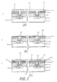
- Fig. 3 illustrates first modification of the production steps of the first embodiment, wherein a silicon dioxide film 2l is added to cover the surface of the polysilicon film 9. This modification is proposed to make ease to determine the end point of the etching back process of Fig. 2(e).
- the process of Figs. 2(a) through 2(c) are same to those of the first embodiment.
- a thin SiO2 layer 2l of approximately 500 A° is formed over the entire surface of the device. Thermal oxidation is preferable for this step.
- the thick polysilicon layer 22 is formed over the entire surface of the device to bury the contact holes as shown in Fig. 3(b).
- the thick polysilicon layer 22 is etched back by conventional dry etching. Since the etching rate of the polysilicon is much larger than that of silicon dioxide, so, it is easy to stop the etching back process correctly at the level of the surface of the thin SiO2 film 2l as shown in Fig. 3(c). After etching off the exposed thin SiO2 film 2l, the process of Fig. 2(d) is followed. So, the final cross section of the device becomes as shown in Fig. 3(d). In Fig. 3(d), the surface of the SiO2 layer 22 is shown to be protruded upward from the level of the polysilicon layer 8 or 9, to emphasis the thickness of the etched SiO2 layer 2l.
- the thickness of the SiO2 2l is only 500 A°, moreover, the polysilicon layer 22 is also etched to some extent by the etchant for the SiO2. Therefore, the top surface of the polysilicon layer 22 is substantially equal to the top surface of the polysilicon layer 8 or 9.
- the material burying the contact holes 22 are replaced by polysilicon, but the effect is same. It should be pointed out that by adding the thin SiO2 film 2l, it becomes possible to replace the material to bury the contact holes to any other materials, such as amorphous silicon for example. And the control of the etching back process becomes easier. It will be understood for the one in the art that the thin SiO2 layer 2l in the process 3(a) may be replaced by some other insulator layer, such as silicon nitride (Si3N4) for example.
- Si3N4 silicon nitride
- Fig. 4 shows second modification of the first embodiment illustrating a cross section of the contact holes corresponding to that of Fig. 2(f), wherein the level of the silicon dioxide layer l0 has been slightly withdrawn from the level of the SiO2 layer 4.
- Such modification is effective when the polysilicon layers 8 and 9 extending over the top surface of the device are removed in order to reduce the contact area to increase the packing density of the devices in the IC.
- Such modification is possible by slightly over etching the SiO2 layer l0 at the process of Fig. 2(e). By such small over etching, there occurs no problem of step covering.
- the configuration of Fig. 4 provides more wide contact area between the polysilicon layers 8 and 9 to the wiring layer ll.
- the thickness of the polysilicon layers 8 and 9 are approximately 2,000 A° corresponding to Fig. 2(d).
- the contact area between the polysilicon layers 8 or 9 and the wiring layer ll is very small.
- the side walls of the polysilicon layers 8 and 9 can be also used as the contact are by the wiring layer ll, so, the contact area is increased by such over etching. And the contact resistance is reduced.
- the second embodiment of the present invention intends to overcome the problem of migration of metals on the polysilicon.
- the migration is avoided by adding a barrier layer between the polysilicon and the metal layer.
- Fig. 5 illustrates a cross sectional view close to the contact holes of the second embodiment. The figure corresponds to Fig. 2(f).
- the second embodiment of Fig. 5 is added a barrier layer denoted by reference numeral l2.
- the barrier layer l2 is composed of silicide of high melting point metal such as tungsten, molybdenum or platinum.
- the barrier layer composes a second conductive layer between the wiring layer ll and the first conductive layer composed of the polysilicon layers 8 and 9.
- barrier layer is deposited by CVD or sputtering. It will be understood for the one skilled in the art, that the deposition of the barrier layer can be done between the steps of 2(e) and 2(f) described with respect to Fig. 2. In an example, tungsten silicide (WSi2) film of approximately l,000 A° has been deposited by CVD. By the barrier layer l2, the migration of the metal has been avoided. Several modifications are possible for the second embodiment described with respect to Fig. 5.
- Fig. 6 shows first modification of the second embodiment. It will be clear for the one in the art that the barrier layer l2 is added to the device shown in Fig. 3(d). Therefore, the deposition of the barrier layer l2 should be done between the steps of 3(c) and 3(d) described with respect to Fig. 3. The effect of preventing the migration of aluminum is further added to the device of Fig. 3(d).
- the barrier layer l2 is composed of a silicide of high melting point metals. But it is possible to avoid the migration of metals by other method.
- the barrier layer is formed by a high melting point metal layer.
- Fig. 7 shows the steps to form the barrier layer composed from metal layer of high melting point metals such as tungsten, molybdenum or platinum. Such material will be denoted as barrier metal hereinafter.
- the process begins following the step 2(c) described with respect to Fig. 2.
- the barrier metal layer 23 of approximately 500 - l,000 A° thick, second thin SiO2 layer 24 of approximately 500 A° and thin polysilicon layer 22 are successively deposited by CVD on the entire surface of the substrate.
- the step coverage of theses layers are very good, because they are deposited by CVD, and the thin polysilicon layer 22 buries the contact holes.
- the polysilicon layer 22 is etched back as shown in Fig. 7(e). Dry etching is applicable for such purpose.
- the etched surface of the substrate is covered with the barrier metal layer 23 ⁇ , over which the wiring layer ll are formed.
- the latter step is similar to the step 2(f) described with respect to Fig. 2.
- the barrier layer 23 and 23 ⁇ are added over the polysilicon layers 8 and 9. These layers not merely provide the effect of preventing the migration of metal over the polysilicon, but they increase the conductivity of the layer to connect between the contact regions 2 or 3 and the wiring layer ll. Since the conductivity of the doped polysilicon is not so high, and its thickness is very thin, the barrier layer becomes a second conducting layer connecting between the contact region and the wiring layer. So, the characteristics of the device is further improved.
- the metal barrier layer is converted to silicide by heat treatment.
- the fabrication process follows the step 7(e) of Fig. 7.
- second barrier metal layer 25 of approximately l,000 A° is formed over the surface of the substrate. CVD or sputtering are applicable for this step.
- the chip is annealed at a temperature of 600 - 800 °C to convert the barrier metal to silicide. So, the second barrier metal layer 25 and polysilicon layer 22 burying the contact hole react to each other and form a silicide layer l6. As can be seen in Fig. 8(a), the reaction occurs only at a potion where the barrier metal is contacted to the silicon (polysilicon). So, the silicide layer l6 is formed only at the portion of the contact holes as shown in Fig. 8(b). Then the remaining second barrier metal layer 25 is selectively etched off. The etching is done by dry etching. When the etching is completed, the appearance becomes as shown in Fig. 8(b).
- the following steps to form the wiring layer ll are similar to those of Fig. 2(f).
- the cross section of the contact holes at the final state becomes as shown in Fig. 8(c).
- wiring layer which is usually aluminum, does not directly contact to silicon (polysilicon), so the migration is avoided.
- the contact between the contact regions 2 or 3 and the wiring layer l0 is secured by double layer of n or p type polysilicon layer 8 or 9 and the barrier metal layer 9. So the conductivity is further improved to that of Fig. 7(f).
- Modification of the third embodiment is also possible, it starts from the process step 3(c) described with respect to Fig. 3(c).
- the thin SiO2 layer 2l is etched off.
- the entire surface is covered with a barrier metal layer (not shown), and chip is annealed to convert the barrier metal layer to silicide.
- the entire top surface of the chip is converted to the silicide and becomes the barrier layer.
- the contact holes formed in an insulation layer are coated its inside with a conductive polysilicon layer having same conductivity type to that of the contact regions of the device fabricated beneath the insulation layer.
- the step coverage of the polysilicon layer is very good because it is formed by chemical vapor deposition. Remaining portion of the contact holes are buried with a burying means which includes silicon dioxide. By doing so, the disconnection of the wiring layer is avoided and the reliability of the wiring is increased. The short circuit caused by growth of spikes formed by eutectic of silicon and metal is also avoided.
- the material composing the burying means which buries the remaining portion of the contact holes may be SiO2. It may be replaced by other materials such as polysilicon or amorphous silicon, but in order to do so, at least a layer of insulation film such as SiO2 or Si3N4 is necessary to cover the surface of the conductive polysilicon layer.
- the present invention further adds a barrier layer between the wiring layer and silicon (it may be polysilicon or amorphous silicon) to prevent the migration of metal (especially aluminum) over the silicon surface.
- This barrier layer becomes second conductive layer to connect between the wiring layer and the contact region of the device. This further increases the conduction between the contact area and the wiring layer.
- the barrier layer is made from silicide of high melting point metal such as tungsten, molybdenum, titanium or platinum. But the barrier layer may be composed of a film of such high melting point metal. By using such material, the conductivity of the wiring layer is further increased. Such increase of conductivity is important for a device operated with high speed or decreasing heat generation of the chip.
- the conductivity type of the substrate have been supposed to be n type, but it will be apparent that the invention may be applied to a substrate having any type of conductivity, and dimensions of the device described with respect to the embodiments are to be considered in all respects as illustrative and not restrictive.
Abstract
Description
- The present invention relates to a configuration of semiconductor devices to improve the reliability of its interconnection wirings formed on the surface of the device. Especially it relates to a configuration of a wiring layers to provide a good step coverage for contact holes formed in an insulation layer through which the wiring layer contacts to the device electrodes.
- In recent semiconductor devices, especially in integrated circuits (ICs) the dimension of the devices fabricated on a chip become very small, while the insulation layer covering the surface of the device cannot be made so thin. So, the openings of contact holes formed in the insulation layer through which the wiring layer contacts to electrodes of the devices become very small. This increases difficulty to contact the wiring layer formed on the surface of the insulation layer to the electrode positioned on the bottom of the contact holes. Because the wiring layer must cover the side walls of the contact holes of the insulator, but it becomes difficult when the opening of the contact hole become comparative to the depth of the contact hole.
- To cover a side wall of stepped portion by wiring material is called in the art as step covering or step coverage. Usually aluminum is sputtered to form the wiring layer over the insulated surface of the devices. The step coverage of sputtered aluminum is poor, so the wiring pattern often breaks and causes disconnection at the stepped portion on the surface of the device on which the wiring layer is formed causing malfunction of the device. In order to overcome such problem, the sputtering is done from various directions so that the side wall of the stepped potion is covered by the wiring material.
- But as mentioned before, when the device size decreases, and the opening of the contact hole becomes comparative to the depth of the hole, the side sputtering becomes ineffective. Such situation is shown in Fig. l, which schematically illustrates a cross section of a device at a portion close to a contact hole. In the figure, a reference numeral 3l designates an n-type silicon substrate for instance, and 32 designates an n⁺-type contact region to be contacted by the wiring layer. 32 may be a contact region for the device (not shown completely), and 33 is a surface coating insulation layer such as silicon dioxide (SiO₂) layer for example. A
contact hole 35 is formed in theinsulation layer 33 through which thewiring layer 34 contacts with thecontact region 32. Thewiring layer 34 is composed of aluminum sputtered on theinsulation layer 33. The sputtering is done vertically and also from slanted directions in the figure. But as can be seen in the figure, the thickness of the aluminum layer on the side walls of the contact hall becomes thin at side walls of thecontact hole 35. Namely, the step coverage of sputtered aluminum is poor, and it often causes disconnection of the wiring layer. - There is another problem in the aluminum wiring layer. Aluminum is liable to form an eutectic alloy with silicon, and it forms spikes which penetrate through the
contact region 32 and causes a short circuit between thewiring layer 34 and the substrate 3l. Several manipulations have been proposed to overcome such problems. - One proposal is to provide a thin layer (approximately 500 A°) of polycrystalline silicon (not shown) between the
aluminum layer 34 and the n⁺contact region 32. By such method, the resistivity of the silicon layer can not be reduced so much, so, recently an alloy of aluminum and silicon, tungsten or titanium is sputtered. Such method is disclosed in, for example, French patent 84093l3 by Joel Alman, June l4, l984 (the same application has been published as Japanese Laid Open Patent 6l-l0256, Jan. l7, l986). But in such methods, the problem of step coverage of the sputtered material still remains. - Another proposal is to bury the contact holes with conductive material such as polysilicon (polycrystalline silicon). In this case, the polysilicon must be doped with p or n type materials in accordance with the conductivity type of the contact regions beneath the polysilicon in order to make a good ohmic contact. If the conductivity type of the contact regions in the chip have all same one conductivity type, the doping can be done in a process to grow the polysilicon layer (chemical vapor deposition for example). But usually, the chip contains both the p and n type contact regions, so the doping must be done selectively in accordance with the conductivity type of the contact regions beneath the polysilicon. Such selective doping must be done by diffusion process from the surface of the grown polysilicon layer. But the conductivity of the diffused layer becomes low as the distance from the surface becomes large. Therefore, the resistivity of the buried material in the contact holes becomes high, and so the resistance of the wiring layer increases. Accordingly, though such method had been proposed, its adoption in practical use was very rare.
- On the contrary, the conductivity of the wiring layer increasing its importance for the device which is operated in high speed or to decrease the heat dissipation of large scale integrated circuits.
- Object of the present invention, therefore, is to provide a semiconductor device of which wiring layer has a good step coverage for contact holes.
- Another object of the present invention is to increase the reliability of semiconductor device by preventing the disconnection and spike through of the wiring layer.
- Still another object of the present invention is to provide a structure of semiconductor device desirable for attaining foregoing objects.
- Further object of the present invention is to provide a fabrication process for realizing foregoing objects.
- According to first embodiment of the present invention, in the contact holes formed of the insulation layer through which the wiring layer contacts to the device electrodes are formed a polysilicon film. The polysilicon film is formed by chemical vapor deposition (CVD), which deposits the material almost uniformly on the surface to be deposited regardless to the direction. Therefore, the side walls of the contact holes are covered with polysilicon film having almost the same thickness to that grown on the top surface of the insulation layer. The polysilicon film at the portion of the contact holes are selectively doped by ion implantation to have the same conductivity to that of respective contact regions. This doped polysilicon film provides a first conductive layer having a good step coverage for the contact holes.
- The portions of the first conductive layer positioned in each contact holes are buried with a thick layer of silicon dioxide (SiO₂), so the surface of the device becomes flat. Over such flat surface, the wiring layer is formed. So, the problem of step coverage and spikes of eutectic material have been avoided, and a good ohmic contact is secured.
- As a variation of the first embodiment, the thick silicon dioxide layer is replace by a thin silicon dioxide layer, and the remaining part of the contact hole is buried with some other materials, such as polysilicon, or amorphous silicon etc. In any case, the polysilicon film should be covered with a silicon dioxide film. The reason will be discussed in the following detailed description of the invention.
- According to the second embodiment of the invention, a barrier layer made from silicide of metals having high melting point (WSi₂ for example) is added on the surface of the polysilicon film described in the first embodiment. This barrier layer prevents the disconnection or decrease of conductivity of wiring layer caused by migration of metal (especially aluminum) on the silicon. The barrier layer is also formed by CVD, so its step coverage is good, and it provides second conductive layer to connect between the contact region and the wiring layer. So, the contact resistance is further decreased.
- According to the third embodiment, the barrier layer is formed by a metal having high melting point, tungsten, molybdenum, or platinum etc. As a modification of the third embodiment, the metal layer is heat treated to form a silicide barrier layer. These and other modifications and advantage of the invention will be described in detail in following description of preferred embodiments.
-
- Fig. l shows schematically a cross section of a device at a portion close to a contact hole illustrating poor step coverage of the wiring layer formed by prior art.
- Fig. 2 shows a cross section of a portion of device close to contact holes illustrating production steps for fabricating a wiring layer of the first embodiment of the present invention.
- Fig. 3 illustrates first modification of the production steps of the first embodiment, wherein a silicon dioxide film 2l is added to cover the surface of the
polysilicon films - Fig. 4 shows second modification of the first embodiment illustrating a cross section of the contact holes corresponding to that of Fig. 2(f), wherein the silicon dioxide layer l0 has been intentionally over etched to secure more good contact of the wiring layer ll to the
polysilicon films - Fig. 5 shows a cross section of a portion of device close to the contact holes illustrating second embodiment of the present invention, wherein a barrier layer l2 is added to prevent the migration of wiring metal ll.
- Fig. 6 shows a variation of the second embodiment, wherein the material burying the contact holes are replaced by thin layer of silicon dioxide 2l and
polysilicon 22 or amorphous silicon. - Fig. 7 illustrates the production steps for third embodiment, wherein the barrier layer is formed by a layer of metal having a high melting temperature.
- Fig. 8 illustrates the production steps for a variation of the third embodiment, disclosing a method to convert the metal barrier layer to a silicide barrier layer.
- Now, the advantage of the present invention will be described referring to preferred embodiments. Fig. 2 illustrates fundamental steps of fabrication process to realize a first embodiment of the present invention. In the disclosure hereinafter a substrate of n type silicon is used as an example. But it will be apparent that the substrate may by replaced by a one having other type of conductivity. In the description hereinafter the steps of the process will be denoted by the same number of the figures. For example, the process described with respect to Fig. 2(a) will be denoted as the process 2(a).
- As shown in Fig. 2(a), the surface of an n type silicon substrate l is covered with an
insulation layer 4 which may be a silicon dioxide layer of l µm thick for example. And over the n⁺ and p⁺type contact regions contact holes - Next, as shown in Fig. 2 (b), over the entire surface of the substrate is deposited a
polysilicon layer 7 of approximately 2,000 A° thick by chemical vapor deposition (CVD). The thickness of thepolysilicon layer 7 may be appropriate l,000 - 3,000 A° for example. As mentioned before, the CVD process deposits a material uniformly over the surface regardless to its inclination. So, the deposited polysilicon layer has almost equal thickness at the side walls and at the top surface of the device. Namely, the step coverage is very good. - Subsequently, as shown in Fig. 2(c), the polysilicon layer at the portion of
contact holes type polysilicon layers type contact regions - Next, as shown in Fig. 2(d), on the surface of the substrate is deposited a thin SiO₂ layer l0 by CVD. The thickness of the SiO₂ layer has enough thickness to bury the contact holes 5 and 6.
- Then as shown in Fig. 2(e), the SiO₂ layer l0 is etched back to expose the surface of the n and p
type polysilicon layers - Succeedingly, as shown in Fig. 2(f), a wiring layer ll is formed over the flat surface of the device. The wiring layer may be fabricated with any kind of material, but aluminum is most popular in the art. The aluminum is sputtered by conventional method, and the aluminum layer ll is patterned by conventional photolithography to a predetermined pattern to interconnect the electrodes. The surface of the device is then passivated by a conventional manner and the device is finished.
- As can be seen in Fig. 2(f), the n and p
type contact regions type polysilicon films polysilicon films contact regions - Above disclosed process for fabricating the first embodiment of the present invention is a fundamental process. But it is possible to make several modifications each having further improvement or advantage over the first embodiment.
- Fig. 3 illustrates first modification of the production steps of the first embodiment, wherein a silicon dioxide film 2l is added to cover the surface of the
polysilicon film 9. This modification is proposed to make ease to determine the end point of the etching back process of Fig. 2(e). The process of Figs. 2(a) through 2(c) are same to those of the first embodiment. Following the process 2(c) of Fig. 2, as shown in Fig. 3(a), a thin SiO₂ layer 2l of approximately 500 A° is formed over the entire surface of the device. Thermal oxidation is preferable for this step. Then thethick polysilicon layer 22 is formed over the entire surface of the device to bury the contact holes as shown in Fig. 3(b). Then thethick polysilicon layer 22 is etched back by conventional dry etching. Since the etching rate of the polysilicon is much larger than that of silicon dioxide, so, it is easy to stop the etching back process correctly at the level of the surface of the thin SiO₂ film 2l as shown in Fig. 3(c). After etching off the exposed thin SiO₂ film 2l, the process of Fig. 2(d) is followed. So, the final cross section of the device becomes as shown in Fig. 3(d). In Fig. 3(d), the surface of theSiO₂ layer 22 is shown to be protruded upward from the level of thepolysilicon layer polysilicon layer 22 is also etched to some extent by the etchant for the SiO₂. Therefore, the top surface of thepolysilicon layer 22 is substantially equal to the top surface of thepolysilicon layer - Compared to the device fabricated by the first modification to that of the first embodiment, the material burying the contact holes 22 are replaced by polysilicon, but the effect is same. It should be pointed out that by adding the thin SiO₂ film 2l, it becomes possible to replace the material to bury the contact holes to any other materials, such as amorphous silicon for example. And the control of the etching back process becomes easier. It will be understood for the one in the art that the thin SiO₂ layer 2l in the process 3(a) may be replaced by some other insulator layer, such as silicon nitride (Si₃N₄) for example.
- Fig. 4 shows second modification of the first embodiment illustrating a cross section of the contact holes corresponding to that of Fig. 2(f), wherein the level of the silicon dioxide layer l0 has been slightly withdrawn from the level of the
SiO₂ layer 4. Such modification is effective when the polysilicon layers 8 and 9 extending over the top surface of the device are removed in order to reduce the contact area to increase the packing density of the devices in the IC. Such modification is possible by slightly over etching the SiO₂ layer l0 at the process of Fig. 2(e). By such small over etching, there occurs no problem of step covering. And it will be clear that the configuration of Fig. 4 provides more wide contact area between the polysilicon layers 8 and 9 to the wiring layer ll. In Fig. 4, the thickness of the polysilicon layers 8 and 9 are approximately 2,000 A° corresponding to Fig. 2(d). Therefore, the contact area between the polysilicon layers 8 or 9 and the wiring layer ll is very small. But as can be seen in Fig. 4, when the level of the SiO₂ layer l0 is slightly withdrawn, the side walls of the polysilicon layers 8 and 9 can be also used as the contact are by the wiring layer ll, so, the contact area is increased by such over etching. And the contact resistance is reduced. - Coming back to Fig. 2(f) that shows a cross section of the first embodiment, the contact area between the wiring layer ll and the
polysilicon films - The second embodiment of the present invention intends to overcome the problem of migration of metals on the polysilicon. The migration is avoided by adding a barrier layer between the polysilicon and the metal layer. Fig. 5 illustrates a cross sectional view close to the contact holes of the second embodiment. The figure corresponds to Fig. 2(f). Compared to that, the second embodiment of Fig. 5 is added a barrier layer denoted by reference numeral l2. The barrier layer l2 is composed of silicide of high melting point metal such as tungsten, molybdenum or platinum. The barrier layer composes a second conductive layer between the wiring layer ll and the first conductive layer composed of the polysilicon layers 8 and 9.
- Such material of barrier layer is deposited by CVD or sputtering. It will be understood for the one skilled in the art, that the deposition of the barrier layer can be done between the steps of 2(e) and 2(f) described with respect to Fig. 2. In an example, tungsten silicide (WSi₂) film of approximately l,000 A° has been deposited by CVD. By the barrier layer l2, the migration of the metal has been avoided. Several modifications are possible for the second embodiment described with respect to Fig. 5.
- Fig. 6 shows first modification of the second embodiment. It will be clear for the one in the art that the barrier layer l2 is added to the device shown in Fig. 3(d). Therefore, the deposition of the barrier layer l2 should be done between the steps of 3(c) and 3(d) described with respect to Fig. 3. The effect of preventing the migration of aluminum is further added to the device of Fig. 3(d).
- In the above disclosure, the barrier layer l2 is composed of a silicide of high melting point metals. But it is possible to avoid the migration of metals by other method. In third embodiment of the present invention, the barrier layer is formed by a high melting point metal layer.
- Fig. 7 shows the steps to form the barrier layer composed from metal layer of high melting point metals such as tungsten, molybdenum or platinum. Such material will be denoted as barrier metal hereinafter. The process begins following the step 2(c) described with respect to Fig. 2.
- As shown in Fig. 7(d), the
barrier metal layer 23 of approximately 500 - l,000 A° thick, secondthin SiO₂ layer 24 of approximately 500 A° andthin polysilicon layer 22 are successively deposited by CVD on the entire surface of the substrate. The step coverage of theses layers are very good, because they are deposited by CVD, and thethin polysilicon layer 22 buries the contact holes. Then, thepolysilicon layer 22 is etched back as shown in Fig. 7(e). Dry etching is applicable for such purpose. Subsequently, as shown in Fig. 7(f), the etched surface of the substrate is covered with the barrier metal layer 23ʹ, over which the wiring layer ll are formed. The latter step is similar to the step 2(f) described with respect to Fig. 2. - Comparing the device of Fig. 7(f) to that of Fig. 6, the
barrier layer 23 and 23ʹ are added over the polysilicon layers 8 and 9. These layers not merely provide the effect of preventing the migration of metal over the polysilicon, but they increase the conductivity of the layer to connect between thecontact regions - As a modification of the third embodiment, the metal barrier layer is converted to silicide by heat treatment. The fabrication process follows the step 7(e) of Fig. 7. As shown in Fig. 8(a), second
barrier metal layer 25 of approximately l,000 A° is formed over the surface of the substrate. CVD or sputtering are applicable for this step. - Next, the chip is annealed at a temperature of 600 - 800 °C to convert the barrier metal to silicide. So, the second
barrier metal layer 25 andpolysilicon layer 22 burying the contact hole react to each other and form a silicide layer l6. As can be seen in Fig. 8(a), the reaction occurs only at a potion where the barrier metal is contacted to the silicon (polysilicon). So, the silicide layer l6 is formed only at the portion of the contact holes as shown in Fig. 8(b). Then the remaining secondbarrier metal layer 25 is selectively etched off. The etching is done by dry etching. When the etching is completed, the appearance becomes as shown in Fig. 8(b). - Then, the following steps to form the wiring layer ll are similar to those of Fig. 2(f). The cross section of the contact holes at the final state becomes as shown in Fig. 8(c). As can be seen in the Fig. 8(c), and wiring layer which is usually aluminum, does not directly contact to silicon (polysilicon), so the migration is avoided. The contact between the
contact regions type polysilicon layer barrier metal layer 9. So the conductivity is further improved to that of Fig. 7(f). - Modification of the third embodiment is also possible, it starts from the process step 3(c) described with respect to Fig. 3(c). The thin SiO₂ layer 2l is etched off. Then the entire surface is covered with a barrier metal layer (not shown), and chip is annealed to convert the barrier metal layer to silicide. In this case the entire top surface of the chip is converted to the silicide and becomes the barrier layer. It will be understood for the one skilled in the art that, when the wiring layer ll is formed on this barrier layer, the device becomes similar to that shown in Fig. 6.
- By the present invention, as have been described above, the contact holes formed in an insulation layer are coated its inside with a conductive polysilicon layer having same conductivity type to that of the contact regions of the device fabricated beneath the insulation layer. The step coverage of the polysilicon layer is very good because it is formed by chemical vapor deposition. Remaining portion of the contact holes are buried with a burying means which includes silicon dioxide. By doing so, the disconnection of the wiring layer is avoided and the reliability of the wiring is increased. The short circuit caused by growth of spikes formed by eutectic of silicon and metal is also avoided.
- The material composing the burying means which buries the remaining portion of the contact holes may be SiO₂. It may be replaced by other materials such as polysilicon or amorphous silicon, but in order to do so, at least a layer of insulation film such as SiO₂ or Si₃N₄ is necessary to cover the surface of the conductive polysilicon layer.
- The present invention further adds a barrier layer between the wiring layer and silicon (it may be polysilicon or amorphous silicon) to prevent the migration of metal (especially aluminum) over the silicon surface. This barrier layer becomes second conductive layer to connect between the wiring layer and the contact region of the device. This further increases the conduction between the contact area and the wiring layer.
- The barrier layer is made from silicide of high melting point metal such as tungsten, molybdenum, titanium or platinum. But the barrier layer may be composed of a film of such high melting point metal. By using such material, the conductivity of the wiring layer is further increased. Such increase of conductivity is important for a device operated with high speed or decreasing heat generation of the chip.
- In the above disclosure, the conductivity type of the substrate have been supposed to be n type, but it will be apparent that the invention may be applied to a substrate having any type of conductivity, and dimensions of the device described with respect to the embodiments are to be considered in all respects as illustrative and not restrictive.
Claims (17)
a semiconductor substrate (l) in which said device is fabricated;
an insulation layer (4) covering the top surface of said substrate (l);
a wiring layer (ll) formed on said insulation layer (4) for connecting electrodes of devices;
plurality of contact regions (2, 3) formed on top surface of said substrate (l) to be connected to said wiring layer (ll);
plurality of contact holes (5, 6) formed in said insulation layer (4) through which said wiring layer (ll) and said contact regions (2, 3) are connected, said contact holes (5, 6) being formed respectively over each of said contact regions (2, 3) to expose said contact regions (2, 3) in respective contact holes (5, 6);
conductive polysilicon layers (7, 8, 9) formed on side wall and surface of said contact region (2, 3) exposed in each of said contact holes (5, 6), one end of said conductive polysilicon layer (7, 8, 9) being contacted to said wiring layer (ll); and
burying means (lO; 2l, 22) for burying the remaining portion of each said contact holes (5, 6), each of said burying means (lO) including at least a portion composed of an insulator composed of silicon dioxide or silicon nitride covering the inner surface of said conductive polysilicon layer (7, 8, 9).
Applications Claiming Priority (8)
| Application Number | Priority Date | Filing Date | Title |
|---|---|---|---|
| JP124815/86 | 1986-05-30 | ||
| JP61124816A JPH065732B2 (en) | 1986-05-30 | 1986-05-30 | Semiconductor device |
| JP61124812A JPH07101689B2 (en) | 1986-05-30 | 1986-05-30 | Method for manufacturing semiconductor device |
| JP12481586A JPS62281467A (en) | 1986-05-30 | 1986-05-30 | Semiconductor device |
| JP124812/86 | 1986-05-30 | ||
| JP124814/86 | 1986-05-30 | ||
| JP61124814A JPS62281451A (en) | 1986-05-30 | 1986-05-30 | Semiconductor device |
| JP124816/86 | 1986-05-30 |
Publications (2)
| Publication Number | Publication Date |
|---|---|
| EP0249780A1 true EP0249780A1 (en) | 1987-12-23 |
| EP0249780B1 EP0249780B1 (en) | 1991-08-14 |
Family
ID=27471066
Family Applications (1)
| Application Number | Title | Priority Date | Filing Date |
|---|---|---|---|
| EP87107759A Expired - Lifetime EP0249780B1 (en) | 1986-05-30 | 1987-05-27 | Semiconductor device with a wiring layer having a good step coverage at contact holes |
Country Status (4)
| Country | Link |
|---|---|
| US (1) | US4833519A (en) |
| EP (1) | EP0249780B1 (en) |
| KR (1) | KR900003618B1 (en) |
| DE (1) | DE3772111D1 (en) |
Cited By (2)
| Publication number | Priority date | Publication date | Assignee | Title |
|---|---|---|---|---|
| EP0305055A1 (en) * | 1987-07-28 | 1989-03-01 | Kabushiki Kaisha Toshiba | Method of manufacturing a semiconductor device |
| DE3915337A1 (en) * | 1989-05-10 | 1990-11-15 | Siemens Ag | Low-ohmic planar contact metallisation prodn. - without spiking or diffusion problems |
Families Citing this family (38)
| Publication number | Priority date | Publication date | Assignee | Title |
|---|---|---|---|---|
| JPH03110837A (en) * | 1989-09-26 | 1991-05-10 | Seiko Instr Inc | Manufacture of semiconductor device |
| US5472912A (en) * | 1989-11-30 | 1995-12-05 | Sgs-Thomson Microelectronics, Inc. | Method of making an integrated circuit structure by using a non-conductive plug |
| JPH0680638B2 (en) * | 1990-07-05 | 1994-10-12 | 株式会社東芝 | Method for manufacturing semiconductor device |
| US5231052A (en) * | 1991-02-14 | 1993-07-27 | Industrial Technology Research Institute | Process for forming a multilayer polysilicon semiconductor electrode |
| JP3118785B2 (en) * | 1991-05-23 | 2000-12-18 | ソニー株式会社 | Method of forming barrier metal structure |
| JP2887985B2 (en) * | 1991-10-18 | 1999-05-10 | 日本電気株式会社 | Semiconductor device and manufacturing method thereof |
| US5387550A (en) * | 1992-02-07 | 1995-02-07 | Micron Technology, Inc. | Method for making a fillet for integrated circuit metal plug |
| US5475266A (en) * | 1992-02-24 | 1995-12-12 | Texas Instruments Incorporated | Structure for microelectronic device incorporating low resistivity straps between conductive regions |
| EP0558304B1 (en) * | 1992-02-28 | 2000-01-19 | STMicroelectronics, Inc. | Method of forming submicron contacts |
| JP2924450B2 (en) * | 1992-05-22 | 1999-07-26 | 日本電気株式会社 | Semiconductor device |
| JP3413876B2 (en) * | 1992-07-08 | 2003-06-09 | セイコーエプソン株式会社 | Semiconductor device |
| KR960001176B1 (en) * | 1992-12-02 | 1996-01-19 | 현대전자산업주식회사 | Semiconductor connection apparatus and the manufacturing |
| US5563089A (en) * | 1994-07-20 | 1996-10-08 | Micron Technology, Inc. | Method of forming a bit line over capacitor array of memory cells and an array of bit line over capacitor array of memory cells |
| US5286675A (en) * | 1993-04-14 | 1994-02-15 | Industrial Technology Research Institute | Blanket tungsten etchback process using disposable spin-on-glass |
| JP2684978B2 (en) * | 1993-11-25 | 1997-12-03 | 日本電気株式会社 | Semiconductor device |
| KR0141165B1 (en) * | 1995-03-08 | 1998-07-15 | 김광호 | Transistor favrication method |
| US5624870A (en) * | 1995-03-16 | 1997-04-29 | United Microelectronics Corporation | Method of contact planarization |
| JP3332773B2 (en) * | 1996-03-15 | 2002-10-07 | シャープ株式会社 | Active matrix substrate and method of manufacturing active matrix substrate |
| US5776833A (en) * | 1996-09-04 | 1998-07-07 | Mosel Vitelic Inc. | Method for forming metal plug |
| KR100249170B1 (en) * | 1997-04-10 | 2000-03-15 | 김영환 | Method for fabricating metal line of semiconductor device |
| US6194313B1 (en) * | 1997-04-30 | 2001-02-27 | Texas Instruments Incorporated | Method for reducing recess for the formation of local interconnect and or plug trench fill for etchback process |
| JPH11154701A (en) * | 1997-11-21 | 1999-06-08 | Mitsubishi Electric Corp | Semiconductor device |
| JPH11260937A (en) * | 1998-03-13 | 1999-09-24 | Mitsubishi Electric Corp | Semiconductor device and manufacture thereof |
| US6452276B1 (en) * | 1998-04-30 | 2002-09-17 | International Business Machines Corporation | Ultra thin, single phase, diffusion barrier for metal conductors |
| US6096626A (en) * | 1998-09-03 | 2000-08-01 | Micron Technology, Inc. | Semiconductor structures and semiconductor processing methods of forming silicon layers |
| US6639261B2 (en) * | 1998-12-08 | 2003-10-28 | Micron Technology, Inc. | Method for forming a low leakage contact in a CMOS imager |
| US6156642A (en) * | 1999-03-23 | 2000-12-05 | United Microelectronics Corp. | Method of fabricating a dual damascene structure in an integrated circuit |
| US6399503B1 (en) * | 2001-01-19 | 2002-06-04 | United Microelectronics Corp. | Method of preventing dishing phenomenon atop a dual damascene structure |
| JP2002289490A (en) * | 2001-03-27 | 2002-10-04 | Toshiba Corp | Semiconductor device |
| KR100382738B1 (en) * | 2001-04-09 | 2003-05-09 | 삼성전자주식회사 | Method for forming metal contact in semiconductor device |
| KR100389927B1 (en) * | 2001-06-07 | 2003-07-04 | 삼성전자주식회사 | Semiconductor device having multilevel interconnections and method for manufacturing the same |
| KR100645068B1 (en) * | 2005-08-01 | 2006-11-10 | 삼성전자주식회사 | Semiconductor device and method of fabricating the same |
| JP5343982B2 (en) * | 2009-02-16 | 2013-11-13 | トヨタ自動車株式会社 | Semiconductor device |
| JP2011210744A (en) * | 2010-03-26 | 2011-10-20 | Toshiba Corp | Semiconductor device, and method of manufacturing the same |
| CN102299177B (en) | 2010-06-22 | 2014-12-10 | 中国科学院微电子研究所 | Manufacturing method of contact and semiconductor device with contact |
| US8461043B2 (en) * | 2011-04-11 | 2013-06-11 | Micron Technology, Inc. | Barrier layer for integrated circuit contacts |
| US20160276156A1 (en) * | 2015-03-16 | 2016-09-22 | Taiwan Semiconductor Manufacturing Company Ltd. | Semiconductor device and manufacturing process thereof |
| US9837350B2 (en) * | 2016-04-12 | 2017-12-05 | International Business Machines Corporation | Semiconductor interconnect structure with double conductors |
Citations (2)
| Publication number | Priority date | Publication date | Assignee | Title |
|---|---|---|---|---|
| EP0100897A2 (en) * | 1982-08-06 | 1984-02-22 | International Business Machines Corporation | Method for contacting a pn junction region |
| EP0170544A1 (en) * | 1984-06-14 | 1986-02-05 | Commissariat A L'energie Atomique | Self-aligning method of forming an interconnection line over a contact hole in an integrated circuit |
Family Cites Families (5)
| Publication number | Priority date | Publication date | Assignee | Title |
|---|---|---|---|---|
| JPS5130437B1 (en) * | 1970-03-25 | 1976-09-01 | ||
| US4329706A (en) * | 1979-03-01 | 1982-05-11 | International Business Machines Corporation | Doped polysilicon silicide semiconductor integrated circuit interconnections |
| US4661832A (en) * | 1982-06-30 | 1987-04-28 | International Business Machines Corporation | Total dielectric isolation for integrated circuits |
| US4526631A (en) * | 1984-06-25 | 1985-07-02 | International Business Machines Corporation | Method for forming a void free isolation pattern utilizing etch and refill techniques |
| US4715109A (en) * | 1985-06-12 | 1987-12-29 | Texas Instruments Incorporated | Method of forming a high density vertical stud titanium silicide for reachup contact applications |
-
1987
- 1987-04-28 KR KR1019870004069A patent/KR900003618B1/en not_active IP Right Cessation
- 1987-05-15 US US07/049,917 patent/US4833519A/en not_active Expired - Fee Related
- 1987-05-27 DE DE8787107759T patent/DE3772111D1/en not_active Expired - Fee Related
- 1987-05-27 EP EP87107759A patent/EP0249780B1/en not_active Expired - Lifetime
Patent Citations (2)
| Publication number | Priority date | Publication date | Assignee | Title |
|---|---|---|---|---|
| EP0100897A2 (en) * | 1982-08-06 | 1984-02-22 | International Business Machines Corporation | Method for contacting a pn junction region |
| EP0170544A1 (en) * | 1984-06-14 | 1986-02-05 | Commissariat A L'energie Atomique | Self-aligning method of forming an interconnection line over a contact hole in an integrated circuit |
Cited By (2)
| Publication number | Priority date | Publication date | Assignee | Title |
|---|---|---|---|---|
| EP0305055A1 (en) * | 1987-07-28 | 1989-03-01 | Kabushiki Kaisha Toshiba | Method of manufacturing a semiconductor device |
| DE3915337A1 (en) * | 1989-05-10 | 1990-11-15 | Siemens Ag | Low-ohmic planar contact metallisation prodn. - without spiking or diffusion problems |
Also Published As
| Publication number | Publication date |
|---|---|
| US4833519A (en) | 1989-05-23 |
| EP0249780B1 (en) | 1991-08-14 |
| KR900003618B1 (en) | 1990-05-26 |
| DE3772111D1 (en) | 1991-09-19 |
| KR870011686A (en) | 1987-12-26 |
Similar Documents
| Publication | Publication Date | Title |
|---|---|---|
| EP0249780A1 (en) | Semiconductor device with a wiring layer having a good step coverage at contact holes | |
| US5330934A (en) | Method of fabricating a semiconductor device having miniaturized contact electrode and wiring structure | |
| EP0279588B1 (en) | Contact in a contact hole in a semiconductor and method of producing same | |
| US4960732A (en) | Contact plug and interconnect employing a barrier lining and a backfilled conductor material | |
| EP0119497B1 (en) | Method of forming electrode/wiring layer | |
| US4822753A (en) | Method for making a w/tin contact | |
| US5144404A (en) | Polysilicon Schottky clamped transistor and vertical fuse devices | |
| EP0097848A1 (en) | Method for manufacturing semiconductor device | |
| JP3067847B2 (en) | Method of forming electrical contact on active layer of MIS integrated circuit | |
| EP0380327A2 (en) | Structure of semiconductor device with funnel-shaped inter-level connection | |
| US4577396A (en) | Method of forming electrical contact to a semiconductor substrate via a metallic silicide or silicon alloy layer formed in the substrate | |
| US5059555A (en) | Method to fabricate vertical fuse devices and Schottky diodes using thin sacrificial layer | |
| EP0076105A2 (en) | Method of producing a bipolar transistor | |
| US5436496A (en) | Vertical fuse device | |
| US4425379A (en) | Polycrystalline silicon Schottky diode array | |
| EP0078501B1 (en) | Transistor-like semiconductor device and method of producing the same | |
| JPH05343404A (en) | Semiconductor device | |
| US5212102A (en) | Method of making polysilicon Schottky clamped transistor and vertical fuse devices | |
| EP0475607B1 (en) | Method of producing semiconductor device including Schottky barrier diode | |
| US4628339A (en) | Polycrystalline silicon Schottky diode array | |
| US4619035A (en) | Method of manufacturing a semiconductor device including Schottky barrier diodes | |
| US6239015B1 (en) | Semiconductor device having polysilicon interconnections and method of making same | |
| EP0272051B1 (en) | Reduced area butting contact structure | |
| JPH03102819A (en) | Manufacture of semiconductor device | |
| JPH05121727A (en) | Semiconductor device and manufacturing method thereof |
Legal Events
| Date | Code | Title | Description |
|---|---|---|---|
| PUAI | Public reference made under article 153(3) epc to a published international application that has entered the european phase |
Free format text: ORIGINAL CODE: 0009012 |
|
| AK | Designated contracting states |
Kind code of ref document: A1 Designated state(s): DE FR GB |
|
| 17P | Request for examination filed |
Effective date: 19880105 |
|
| 17Q | First examination report despatched |
Effective date: 19900131 |
|
| GRAA | (expected) grant |
Free format text: ORIGINAL CODE: 0009210 |
|
| AK | Designated contracting states |
Kind code of ref document: B1 Designated state(s): DE FR GB |
|
| REF | Corresponds to: |
Ref document number: 3772111 Country of ref document: DE Date of ref document: 19910919 |
|
| ET | Fr: translation filed | ||
| PLBE | No opposition filed within time limit |
Free format text: ORIGINAL CODE: 0009261 |
|
| STAA | Information on the status of an ep patent application or granted ep patent |
Free format text: STATUS: NO OPPOSITION FILED WITHIN TIME LIMIT |
|
| 26N | No opposition filed | ||
| PGFP | Annual fee paid to national office [announced via postgrant information from national office to epo] |
Ref country code: FR Payment date: 19960510 Year of fee payment: 10 |
|
| PGFP | Annual fee paid to national office [announced via postgrant information from national office to epo] |
Ref country code: GB Payment date: 19960520 Year of fee payment: 10 |
|
| PGFP | Annual fee paid to national office [announced via postgrant information from national office to epo] |
Ref country code: DE Payment date: 19960528 Year of fee payment: 10 |
|
| PG25 | Lapsed in a contracting state [announced via postgrant information from national office to epo] |
Ref country code: GB Effective date: 19970527 |
|
| GBPC | Gb: european patent ceased through non-payment of renewal fee |
Effective date: 19970527 |
|
| PG25 | Lapsed in a contracting state [announced via postgrant information from national office to epo] |
Ref country code: FR Free format text: LAPSE BECAUSE OF NON-PAYMENT OF DUE FEES Effective date: 19980130 |
|
| PG25 | Lapsed in a contracting state [announced via postgrant information from national office to epo] |
Ref country code: DE Free format text: LAPSE BECAUSE OF NON-PAYMENT OF DUE FEES Effective date: 19980203 |
|
| REG | Reference to a national code |
Ref country code: FR Ref legal event code: ST |