EP0249281B1 - Television picture display device - Google Patents
Television picture display device Download PDFInfo
- Publication number
- EP0249281B1 EP0249281B1 EP87201037A EP87201037A EP0249281B1 EP 0249281 B1 EP0249281 B1 EP 0249281B1 EP 87201037 A EP87201037 A EP 87201037A EP 87201037 A EP87201037 A EP 87201037A EP 0249281 B1 EP0249281 B1 EP 0249281B1
- Authority
- EP
- European Patent Office
- Prior art keywords
- signal
- circuit
- field
- input
- picture
- Prior art date
- Legal status (The legal status is an assumption and is not a legal conclusion. Google has not performed a legal analysis and makes no representation as to the accuracy of the status listed.)
- Expired - Lifetime
Links
Images

Classifications
-
- H—ELECTRICITY
- H04—ELECTRIC COMMUNICATION TECHNIQUE
- H04N—PICTORIAL COMMUNICATION, e.g. TELEVISION
- H04N5/00—Details of television systems
- H04N5/44—Receiver circuitry for the reception of television signals according to analogue transmission standards
- H04N5/445—Receiver circuitry for the reception of television signals according to analogue transmission standards for displaying additional information
- H04N5/45—Picture in picture, e.g. displaying simultaneously another television channel in a region of the screen
-
- H—ELECTRICITY
- H04—ELECTRIC COMMUNICATION TECHNIQUE
- H04N—PICTORIAL COMMUNICATION, e.g. TELEVISION
- H04N5/00—Details of television systems
- H04N5/222—Studio circuitry; Studio devices; Studio equipment
- H04N5/262—Studio circuits, e.g. for mixing, switching-over, change of character of image, other special effects ; Cameras specially adapted for the electronic generation of special effects
- H04N5/265—Mixing
Definitions
- the invention relates to a television picture display device comprising a picture display tube having a scanning circuit which can be synchronized by a first horizontal synchronizing signal and a first vertical synchronizing signal from a first video signal source for obtaining a main picture display of a first video signal obtained from the first video signal source, and a sub-picture change-over switch which can be operated by a switching signal for alternately applying the first video signal or a sub-picture signal to the picture display tube, said sub-picture signal being obtained by means of a compression circuit from a second video signal supplied by a second video signal source, the compression circuit comprising a field memory having a write and a read circuit, which write circuit can be synchronized by a second vertical synchronizing signal obtained from the second video signal source and by a second horizontal synchronizing signal divided in frequency by a divider circuit.
- a television picture display device of the type described above is known from IEEE Transactions on Consumer Electronics, February 1979, pages 512-519.
- the information of the sub-picture displayed during one and the same field of the main picture mostly originates partly from the actual field and partly from the previous field of the second video signal source. This causes disturbing phenomena such as, for example, fringes on oblique picture elements.
- the invention is as set-out in the claims.
- the precharacterising part of claim 1 is based on US-A-4 249 213 disclosing a picture-in-picture television receiver with interlace correction.
- the interlacing correction circuit can accordingly perform a position correction in the displayed sub-picture so that the disturbing phenomena have disappeared.
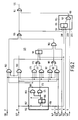
- a first video signal source 1 supplies a first video signal from an output 3, a first horizontal synchronizing signal from an output 5 and a first vertical synchronizing signal from an output 7.
- the first video signal source 1 may be, for example, a receiver section of a television receiver, a television camera or a video recorder.
- the first video signal is applied from the output 3 of the first video signal source 1 to an input of a sub-picture change-over switch 9 which receives at another input a sub-picture signal obtained from an output 11 of a compression circuit 13.
- An output of the sub-picture change-over switch 9 applies a video signal to be displayed to a picture display tube 15.
- the first horizontal sychronizing signal and the first vertical synchronizing signal are applied from the outputs 5 and 7 of the first video signal source 1 to inputs 17 and 19, respectively, of a scanning circuit 21 which, together with the first video signal provides for a main picture display on the picture display tube 15.
- the sub-picture change-over switch 9 is periodically switched to the state not shown during a part of each field period of the main picture by a switching signal applied to an operating signal input 23 of the sub-picture change-over switch 9.
- the compression circuit 13 has an input 25 which receives a second video signal from an output 27 of a second video signal source 29.
- the second video signal source 29 also applies a second horizontal synchronizing signal to an output 31 and a second vertical synchronizing signal to an output 33.
- the second video signal source 29 may be, for example, a possibly second receiver section of a television receiver, a television camera or a video recorder.
- the compression circuit 13 comprises a field memory 35 having a read circuit constituted by a read addressing circuit 37 and a digital-to-analog converter 39 and a write circuit comprising a write addressing circuit 41, a line buffer memory 43 and an analog-to-digital converter 45.
- the input 25 and the output 11 of the compression circuit 13 is also the input of the analog-to-digital converter 45 and the output of the digital-to-analog converter 39, respectively.
- the analog-to-digital converter 45 applies via a signal path 47 a digitalized second video signal to the line buffer memory 43 which supplies a digital second video signal via a signal path 49 to the field memory 35, which video signal is suitable to be written into this memory.
- the field memory 35 then applies a compressed digital second video signal via a signal path 51 to the digital-to-analog converter 39 which forms the sub-picture signal therefrom and supplies this signal from its output 11.
- the outputs 31 and 33 of the second video signal source 29 are connected to inputs 51 and 53, respectively, of a first even-odd field identification circuit 55 an output 57 of which supplies even-odd field information in the form of a logic one or a logic zero signal dependent on the fact whether the second video signal at the output 27 of the second video signal source 29 originates from an even or an odd field.
- This even-odd field information is applied via the signal path 49 to the field memory 35 and continuously written therein.
- An even field is herein to be understood to mean the picture field located in a high position and an odd field is to be understood to mean the picture field located in a low position of a frame. These fields will hereinafter also be referred to as first and second fields, respectively.
- the even-odd field identification circuit may be formed, for example, in known manner or it may be of a type as described in Netherlands Patent Application 8601062 (PHN 11.733).
- the output 57 of the first even-odd field identification circuit 55 is also connected to an operating signal input 59 of a switchable digit generator 61 supplying the digit one during one field and the digit two during the other field to a count-write input 63 of a three-to-one divider 65 which is formed as a counter and a counting signal input 67 of which is connected to the output 31 for the second horizontal synchronizing signal, whilst a write command signal input 69 is connected to the output 33 for the second vertical synchronizing signal from the second video signal source 29.
- the digit generator 61 and the three-to-one divider 65 constitute an interlacing circuit 71 whose output 73 connected to an output of the three-to-one divider 65 supplies a pulse to an input 75 of a write addressing circuit 77 of the line buffer memory 43 each time at the commencement of a line to be written into said line buffer memory.
- a write clock signal input 79 of the write addressing circuit 77 of the line buffer memory 43 is connected to an output 83 of a first clock signal generator 85 whose frequency is coupled to that of the second horizontal synchronizing signal by means of a coupling circuit 87.
- a read clock signal input 89 of a read address circuit 91 of the line buffer memory 43 is connected to an output 93 of a second clock signal generator 94 which, by means of a coupling circuit 95, is coupled in frequency to the first horizontal synchronizing signal originating from the output 5 of the first video signal source 1.
- the active field period in which the field memory 35 is written via the line buffer memory 43 is derived by the write addressing circuit 41 of the field memory 35 from the second vertical synchronizing signal applied to an input 96 thereof and originating from the output 33 of the second video signal source 29.
- a signal representing this active field period is applied by an output 97 of the write addressing circuit 41 of the field memory 35 to an input 98 of the write addressing circuit 77 of the line buffer memory 43.
- the switching signal which is applied to the input 23 of the sub-picture change-over switch 9 and which originates from an output 99 of the read address circuit 37 of the field memory 35 and which will hereinafter be denoted by P, is also applied to an interruption signal input 101 of the read address circuit 91 of the line buffer memory 43 and to an interruption signal input 103 of the write addressing circuit 41 of the field memory 35.
- the line buffer memory 43 is written each time during a line period of the second video signal source 29 whereafter there is time during two line periods to transfer its contents to the field memory 35 in the periods when there is no display from the field memory 35. Transferring is started immediately after writing. To this end a signal is applied from an output 105 of the write addressing circuit 77 of the line buffer memory 43 to an input 107 of the read address circuit 91 of the line buffer memory 43 and to an input 109 of the write addressing circuit 41 of the field memory 35.
- the even-odd field information originating from the output 57 of the first even-odd field identification circuit 55 is also applied to the signal path 49 leading to the field memory 35 so that per sample of the signal written into the field memory 35 a bit is present which indicates whether the relevant sample originates from an even or from an odd field of the second video signal source 29.
- the writing of the field memory 35 is organised in such a manner that it cannot be interrupted at an arbitrary instant of a line period of the second video signal source 29, as is indeed the case here, it is sufficient to write the even-odd field information each time at the commencement of a line period.
- the read address circuit 37 thereof is synchronized with the scanning circuit 21 of the picture display tube 15 via inputs 111 and 113 connected to the outputs 5 and 7, respectively, of the first video signal source 1 so that the sub-picture is displayed in a desired position in the main picture.
- the outputs 5 and 7 of the first video signal source 1 also apply the first horizontal synchronizing signal to imputs 115 and 117, respectively, of a second even-odd field identification circuit 119, from which synchronizing signals an even-odd field information D of the main picture is derived which is applied via an output 121 of the second even-odd field identification circuit 119 to an input 123 of an interlacing-correction circuit 125 a further input 127 of which receives the even-odd field information A of the sub-picture from the signal path 51 during reading of the field memory 35.
- the interlacing-correction circuit 125 applies a pulse via an output 129 thereof to an input 131 of the read addressing circuit 37 of the field memory 35 at given instants which will be further described hereinafter, which pulse causes an address counter of this read address circuit 37 to make an extra step.
- This is the simplest manner of read address correction. It is of course alternatively possible to perform both positive and negative read address corrections. This is, however, generally difficult to perform because there are generally no connections on the address circuit available for this purpose.
- the said pulse is derived from the signals A and D by means of a number of signals P, S, N, L which are obtained from outputs 99, 133, 135, 137, respectively, of the read address circuit 37 of the field memory 35 and which are applied to inputs 139, 141, 143, 145, respectively, of the interlacing-correction circuit 125.
- a clock signal input 47 of the interlacing-correction circuit 125 receives the second clock signal C from the output 93 of the second clock signal generator 94.
- corresponding components have the same reference numerals as in Figure 1 and the clock signal input 147 of the interlacing-correction circuit 125 is connected to a clock signal input 151 of a field transition detection circuit 153 which is connected to the clock signal input of a D flip-flop 155 whose D input is connected via an input 157 of the field transition detection circuit 153 to the input 127 of the interlacing-correction circuit 125 for the even-odd field information A of the sub-picture.
- the Q output of the D flip-flop 155 applies a signal B to an inverting input of an AND gate 159 which is delayed by one clock signal pulse period with respect to the signal A.
- the other input of the AND gate 159 is connected to the input 157 of the field transition detection circuit 153, and the output of the AND gate 159 is connected to an output 161 of the field transition detection circuit 153.
- the AND gate 159 supplies a pulse AB' from the output 161, which pulse covers one clock signal period when there is an odd-even field transition. In this case it was assumed that an even field of the sub-picture corresponds to a value of the signal A which is logic one and that the even field of the sub-picture is originally located in a higher position than the odd field.
- the displayed even portion would acquire a lower position after the transition than the displayed odd portion before the transition.
- the signal at the output 161 of the field transition detection circuit 153 is applied to an AND gate 163 a further input of which receives the signal P from the input 139 and an inverting input is connected to the input 141 to which the signal S is applied.
- the signal S is high during a clock signal period at the commencement of the sub-picture, consequently during the first clock signal period of the signal P in a field of the main picture.
- the AND gate 163 supplies a pulse which is applied via an OR gate 165 and an OR gate 167 to the output 129 of the interlacing-correction circuit 125 so that the read address of the field memory undergoes an extra increase of one step and the portion of the sub-picture displayed after the odd-even transition is raised in position and is brought to the correct position with respect to the odd portion.
- the next main picture field in which the sub-picture occurred with the odd-even transition was an even field
- the next main picture field is odd and the sub-picture therein will have an even-odd transition.
- the upper even portion of the sub-picture is then positioned too low with respect to the odd field of the main picture and is raised in position by an extra step at the commencement of the sub-picture in response to an extra pulse supplied by an AND gate 169 connected to a further input of the OR gate 165, whilst a first input of said AND gate receives the signal S, a second input receives the signal A and a third inverting input receives the signal D, i.e. the even-odd field information of the main picture which is one when the relevant field of the main picture is even.
- the next main picture field is an even field in which an even-odd sub-picture transition takes place and in which the position need not be corrected because the upper portions of the fields have a correct location with respect to each other and because there is no change of position at the sub-picture field transition.
- the field transition detection circuit 153 includes an AND gate 171 an input of which receives the signal B from the Q output of the D flip-flop 155 and an inverting input is connected to the input 157 of the transition detection circuit 153.
- the output of the AND gate 171 is connected to an output 173 of the field transition detection circuit 153 and supplies a pulse during one clock signal period in the event of an even-odd field transition of the sub-picture.
- the output 161 of the field transition detection circuit 153 is also connected to an input of an AND gate 175 a second input of which is connected to the input 123 and a third input of which is connected to the input 139 of the interlacing-correction circuit 125.
- the output 173 of the field transition detection circuit 153 is connected to a first input of an AND gate 177 an inverting second input of which is connected to the input 123 and a third input of which is connected to te input 139 of the interlacing-correction circuit 125.
- the outputs of the AND gates 175 and 177 are connected to the input of an OR gate 179 the output of which is connected to the set input of a set-reset flip-flop 181 the reset input of which receives the signal S from the input 141 of the interlacing-correction circuit 125 and the Q output of which is connected to an input of an AND gate 183 the output of which is connected to the third input of the OR gate 165.
- the clock signal input of the set-reset flip-flop 181 is connected to the clock signal input 147 of the interlacing-correction circuit 125.
- a second input of the AND gate 183 is connected to the output of an OR gate 185 and a third input is connected to the input 141 of the interlacing-correction circuit 125.
- the inputs of the OR-gate 185 are connected to the outputs of two AND-gates 187, 189.
- the inputs of the AND-gate 187 receive the signals A, D and P from the inputs 127, 123, 139, respectively, of the interlacing-correction circuit 125.
- An input of the AND gate 189 is connected to the input 139 of the interlacing-correction circuit 125 for the signal P and its two inverting inputs are connected to the input 127 for the signal A and to the input 123 for the signal D of the interlacing-correction circuit 125.
- the set-reset flipflop 181 is reset by the clock signal each time at the trailing edge of the signal S so that this flipflop 181 can only apply a logic one signal to the AND gate 183 until the end of the signal S when in the previous field of the main picture the OR gate 179 had supplied a logic one signal during the main picture. This is the case due to the operation of the AND gate 175 when the main picture field was even and when an odd-even field transition had occurred in the sub-picture, or due to the operation of the AND gate 177 when the main picture was odd and when an even-odd field transition had occurred in the sub-picture.
- the AND gate 183 can then supply a logic one signal during the occurrence of the signal S at the commencement of a sub-picture if also the OR gate 185 supplies a logic one signal, which is the case when the main picture field and the sub-picture field are both even or both odd. This only occurs when the field transition of the sub-picture is displaced to the commencement thereof and is located so close to the commencement thereof that no field transition occurs in the sub-picture during the next field. Due to this measure it is even possible to display in an undisturbed manner a sub-picture originating from a 60 Hz video signal source in a main picture of a 50 Hz video signal source, or conversely.
- the OR gate 165 thus applies a logic one signal to the OR gate 167, which signal is also applied to an input 191 of a sub-picture end correction circuit 193 which is also the set input of a set-reset flipflop 195 whose Q output is connected to an input of an AND gate 197 whose output 199 is also the output of the sub-picture end correction circuit 193.
- This signal N is a pulse which occurs in the clock signal period preceding the signal S, hence in the clock signal period prior to the commencement of the sub-picture so that the set-reset flipflop 195 is reset prior to the commencement of each sub-picture.
- a fourth input 203 of the sub-picture end correction circuit 193 receives the signal L from the input 145 of the interlacing-correction circuit 125.
- This signal L is a pulse which occurs in the last clock signal period of the penultimate line of the sub-picture.
- the Q output of this set-reset flipflop 195 is still logic one and the AND gate 197 as yet applies a logic one signal to the output 199 of the sub-picture end correction circuit at the end of the penultimate line of the sub-picture, which logic one signal produces an address correction via the OR gate 167 so that the end of the sub-picture occurs in the same position in the main picture as in the cases when an address correction signal is supplied by the OR gate 165 so that troublesome jumping of the end of the sub-picture cannot occur.
- the interlacing circuit 71 can be formed in a simpler manner by writing only once per two fields a suitable value into the counter 65 via the count input 63.
- the digital-to-analog converter 39 can be incorporated after the sub-picture change-over switch 39, if desired, if the first and the second video signal have the same digital structure.
- the even-odd field identification circuits 55 and 119 may each form part, if desired, of for example a synchronizing signal pattern correction circuit as described in the previously mentioned Netherlands patent application 8601062, which circuits can then apply the relevant synchronizing signals to the inputs 67 and 69 of the interlacing circuit 71 and to the input 96 of the write addressing circuit 41 of the field memory 35 and to the inputs 111 and 113 of the read addressing circuit 37 of the field memory 35 and to the inputs 17 and 19 of the scanning circuit 21, respectively.
Description
- The invention relates to a television picture display device comprising a picture display tube having a scanning circuit which can be synchronized by a first horizontal synchronizing signal and a first vertical synchronizing signal from a first video signal source for obtaining a main picture display of a first video signal obtained from the first video signal source, and a sub-picture change-over switch which can be operated by a switching signal for alternately applying the first video signal or a sub-picture signal to the picture display tube, said sub-picture signal being obtained by means of a compression circuit from a second video signal supplied by a second video signal source, the compression circuit comprising a field memory having a write and a read circuit, which write circuit can be synchronized by a second vertical synchronizing signal obtained from the second video signal source and by a second horizontal synchronizing signal divided in frequency by a divider circuit.
- A television picture display device of the type described above is known from IEEE Transactions on Consumer Electronics, February 1979, pages 512-519.
- Since the video signal sources are generally not synchronized, the information of the sub-picture displayed during one and the same field of the main picture mostly originates partly from the actual field and partly from the previous field of the second video signal source. This causes disturbing phenomena such as, for example, fringes on oblique picture elements.
- It is an object of the invention to mitigate these disturbing phenomena.
- The invention is as set-out in the claims. The precharacterising part of claim 1 is based on US-A-4 249 213 disclosing a picture-in-picture television receiver with interlace correction.
- Due to the measures according to the invention it can be established by means of the transferred even-odd field information whether the portion of the sub-picture to be displayed is associated with a field which is located in a high position or with a field in a low position and the interlacing correction circuit can accordingly perform a position correction in the displayed sub-picture so that the disturbing phenomena have disappeared.
- The invention will now be described with reference to the drawing.
- In the drawing
- Figure 1 illustrates by way of a block diagram a television picture display device according to the invention and
- Figure 2 illustrates by way of a principle circuit diagram a favourable embodiment of an interlacing-correction circuit for a television picture display device according to the invention.
- In Figure 1 a first video signal source 1 supplies a first video signal from an
output 3, a first horizontal synchronizing signal from anoutput 5 and a first vertical synchronizing signal from anoutput 7. The first video signal source 1 may be, for example, a receiver section of a television receiver, a television camera or a video recorder. - The first video signal is applied from the
output 3 of the first video signal source 1 to an input of a sub-picture change-overswitch 9 which receives at another input a sub-picture signal obtained from anoutput 11 of acompression circuit 13. An output of the sub-picture change-overswitch 9 applies a video signal to be displayed to apicture display tube 15. - For the sake of clarity the Figure shows the relevant signal paths in a single form. It will be evident that multiple signal paths are used in a colour television picture display device.
- The first horizontal sychronizing signal and the first vertical synchronizing signal are applied from the
outputs inputs scanning circuit 21 which, together with the first video signal provides for a main picture display on thepicture display tube 15. - For the display of a sub-picture the sub-picture change-over
switch 9 is periodically switched to the state not shown during a part of each field period of the main picture by a switching signal applied to anoperating signal input 23 of the sub-picture change-overswitch 9. - The
compression circuit 13 has an input 25 which receives a second video signal from anoutput 27 of a secondvideo signal source 29. The secondvideo signal source 29 also applies a second horizontal synchronizing signal to anoutput 31 and a second vertical synchronizing signal to anoutput 33. The secondvideo signal source 29 may be, for example, a possibly second receiver section of a television receiver, a television camera or a video recorder. - The
compression circuit 13 comprises afield memory 35 having a read circuit constituted by a read addressingcircuit 37 and a digital-to-analog converter 39 and a write circuit comprising a writeaddressing circuit 41, aline buffer memory 43 and an analog-to-digital converter 45. The input 25 and theoutput 11 of thecompression circuit 13 is also the input of the analog-to-digital converter 45 and the output of the digital-to-analog converter 39, respectively. The analog-to-digital converter 45 applies via a signal path 47 a digitalized second video signal to theline buffer memory 43 which supplies a digital second video signal via asignal path 49 to thefield memory 35, which video signal is suitable to be written into this memory. Thefield memory 35 then applies a compressed digital second video signal via asignal path 51 to the digital-to-analog converter 39 which forms the sub-picture signal therefrom and supplies this signal from itsoutput 11. - The
outputs video signal source 29 are connected toinputs field identification circuit 55 anoutput 57 of which supplies even-odd field information in the form of a logic one or a logic zero signal dependent on the fact whether the second video signal at theoutput 27 of the secondvideo signal source 29 originates from an even or an odd field. This even-odd field information is applied via thesignal path 49 to thefield memory 35 and continuously written therein. An even field is herein to be understood to mean the picture field located in a high position and an odd field is to be understood to mean the picture field located in a low position of a frame. These fields will hereinafter also be referred to as first and second fields, respectively. The even-odd field identification circuit may be formed, for example, in known manner or it may be of a type as described in Netherlands Patent Application 8601062 (PHN 11.733). - The
output 57 of the first even-oddfield identification circuit 55 is also connected to anoperating signal input 59 of aswitchable digit generator 61 supplying the digit one during one field and the digit two during the other field to a count-writeinput 63 of a three-to-onedivider 65 which is formed as a counter and acounting signal input 67 of which is connected to theoutput 31 for the second horizontal synchronizing signal, whilst a writecommand signal input 69 is connected to theoutput 33 for the second vertical synchronizing signal from the secondvideo signal source 29. Thedigit generator 61 and the three-to-onedivider 65 constitute aninterlacing circuit 71 whoseoutput 73 connected to an output of the three-to-onedivider 65 supplies a pulse to aninput 75 of a writeaddressing circuit 77 of theline buffer memory 43 each time at the commencement of a line to be written into said line buffer memory. - Likewise as a
clock signal input 81 of the analog-to-digital converter 45, a writeclock signal input 79 of the writeaddressing circuit 77 of theline buffer memory 43 is connected to anoutput 83 of a firstclock signal generator 85 whose frequency is coupled to that of the second horizontal synchronizing signal by means of acoupling circuit 87. - Likewise as a
clock signal input 92 of thefield memory 35 and the write and read addressingcircuits clock signal input 89 of aread address circuit 91 of theline buffer memory 43 is connected to anoutput 93 of a secondclock signal generator 94 which, by means of acoupling circuit 95, is coupled in frequency to the first horizontal synchronizing signal originating from theoutput 5 of the first video signal source 1. - The active field period in which the
field memory 35 is written via theline buffer memory 43 is derived by the writeaddressing circuit 41 of thefield memory 35 from the second vertical synchronizing signal applied to aninput 96 thereof and originating from theoutput 33 of the secondvideo signal source 29. A signal representing this active field period is applied by anoutput 97 of the writeaddressing circuit 41 of thefield memory 35 to aninput 98 of the writeaddressing circuit 77 of theline buffer memory 43. - When the sub-picture is displayed the
field memory 35 is not written from theline buffer memory 43. To this end the switching signal, which is applied to theinput 23 of the sub-picture change-overswitch 9 and which originates from anoutput 99 of theread address circuit 37 of thefield memory 35 and which will hereinafter be denoted by P, is also applied to aninterruption signal input 101 of theread address circuit 91 of theline buffer memory 43 and to aninterruption signal input 103 of thewrite addressing circuit 41 of thefield memory 35. - The
line buffer memory 43 is written each time during a line period of the secondvideo signal source 29 whereafter there is time during two line periods to transfer its contents to thefield memory 35 in the periods when there is no display from thefield memory 35. Transferring is started immediately after writing. To this end a signal is applied from anoutput 105 of the writeaddressing circuit 77 of theline buffer memory 43 to aninput 107 of theread address circuit 91 of theline buffer memory 43 and to aninput 109 of the writeaddressing circuit 41 of thefield memory 35. - The even-odd field information, hereinafter also denoted by A, originating from the
output 57 of the first even-oddfield identification circuit 55 is also applied to thesignal path 49 leading to thefield memory 35 so that per sample of the signal written into the field memory 35 a bit is present which indicates whether the relevant sample originates from an even or from an odd field of the secondvideo signal source 29. When the writing of thefield memory 35 is organised in such a manner that it cannot be interrupted at an arbitrary instant of a line period of the secondvideo signal source 29, as is indeed the case here, it is sufficient to write the even-odd field information each time at the commencement of a line period. - For the purpose of reading the
field memory 35 theread address circuit 37 thereof is synchronized with thescanning circuit 21 of thepicture display tube 15 viainputs outputs - The
outputs field identification circuit 119, from which synchronizing signals an even-odd field information D of the main picture is derived which is applied via anoutput 121 of the second even-oddfield identification circuit 119 to aninput 123 of an interlacing-correction circuit 125 afurther input 127 of which receives the even-odd field information A of the sub-picture from thesignal path 51 during reading of thefield memory 35. - The interlacing-
correction circuit 125 applies a pulse via anoutput 129 thereof to aninput 131 of the read addressingcircuit 37 of thefield memory 35 at given instants which will be further described hereinafter, which pulse causes an address counter of thisread address circuit 37 to make an extra step. This is the simplest manner of read address correction. It is of course alternatively possible to perform both positive and negative read address corrections. This is, however, generally difficult to perform because there are generally no connections on the address circuit available for this purpose. The said pulse is derived from the signals A and D by means of a number of signals P, S, N, L which are obtained fromoutputs read address circuit 37 of thefield memory 35 and which are applied toinputs correction circuit 125. A clock signal input 47 of the interlacing-correction circuit 125 receives the second clock signal C from theoutput 93 of the secondclock signal generator 94. - The function of the above-mentioned signals and a favourable embodiment of an interlacing-correction circuit suitable for supplying the above-mentioned pulses for an extra step of the read address circuit as defined above will be elaborated with reference to Figure 2.
- In Figure 2 corresponding components have the same reference numerals as in Figure 1 and the
clock signal input 147 of the interlacing-correction circuit 125 is connected to aclock signal input 151 of a fieldtransition detection circuit 153 which is connected to the clock signal input of a D flip-flop 155 whose D input is connected via aninput 157 of the fieldtransition detection circuit 153 to theinput 127 of the interlacing-correction circuit 125 for the even-odd field information A of the sub-picture. The Q output of the D flip-flop 155 applies a signal B to an inverting input of anAND gate 159 which is delayed by one clock signal pulse period with respect to the signal A. The other input of theAND gate 159 is connected to theinput 157 of the fieldtransition detection circuit 153, and the output of theAND gate 159 is connected to anoutput 161 of the fieldtransition detection circuit 153. The ANDgate 159 supplies a pulse AB' from theoutput 161, which pulse covers one clock signal period when there is an odd-even field transition. In this case it was assumed that an even field of the sub-picture corresponds to a value of the signal A which is logic one and that the even field of the sub-picture is originally located in a higher position than the odd field. - At an odd-even transition in the sub-picture the displayed even portion would acquire a lower position after the transition than the displayed odd portion before the transition. To prevent this, the signal at the
output 161 of the fieldtransition detection circuit 153 is applied to an AND gate 163 a further input of which receives the signal P from theinput 139 and an inverting input is connected to theinput 141 to which the signal S is applied. The signal S is high during a clock signal period at the commencement of the sub-picture, consequently during the first clock signal period of the signal P in a field of the main picture. - At an odd-even field transition, which occurs in the sub-picture after the first clock period thereof, the
AND gate 163 supplies a pulse which is applied via anOR gate 165 and anOR gate 167 to theoutput 129 of the interlacing-correction circuit 125 so that the read address of the field memory undergoes an extra increase of one step and the portion of the sub-picture displayed after the odd-even transition is raised in position and is brought to the correct position with respect to the odd portion. - If the main picture field in which the sub-picture occurred with the odd-even transition was an even field, the next main picture field is odd and the sub-picture therein will have an even-odd transition. The upper even portion of the sub-picture is then positioned too low with respect to the odd field of the main picture and is raised in position by an extra step at the commencement of the sub-picture in response to an extra pulse supplied by an
AND gate 169 connected to a further input of theOR gate 165, whilst a first input of said AND gate receives the signal S, a second input receives the signal A and a third inverting input receives the signal D, i.e. the even-odd field information of the main picture which is one when the relevant field of the main picture is even. - If the main picture field in which the sub-picture occurred with the odd-even transition was an odd field, the next main picture field is an even field in which an even-odd sub-picture transition takes place and in which the position need not be corrected because the upper portions of the fields have a correct location with respect to each other and because there is no change of position at the sub-picture field transition.
- In principle the AND
gates transition detection circuit 153 may suffice. - The further components of the interlacing-correction circuit of Figure 2 are refinements which perform additional corrections in given cases.
- To this end the field
transition detection circuit 153 includes an ANDgate 171 an input of which receives the signal B from the Q output of the D flip-flop 155 and an inverting input is connected to theinput 157 of thetransition detection circuit 153. The output of the ANDgate 171 is connected to anoutput 173 of the fieldtransition detection circuit 153 and supplies a pulse during one clock signal period in the event of an even-odd field transition of the sub-picture. - The
output 161 of the fieldtransition detection circuit 153 is also connected to an input of an AND gate 175 a second input of which is connected to theinput 123 and a third input of which is connected to theinput 139 of the interlacing-correction circuit 125. - The
output 173 of the fieldtransition detection circuit 153 is connected to a first input of an ANDgate 177 an inverting second input of which is connected to theinput 123 and a third input of which is connected tote input 139 of the interlacing-correction circuit 125. - The outputs of the AND
gates OR gate 179 the output of which is connected to the set input of a set-reset flip-flop 181 the reset input of which receives the signal S from theinput 141 of the interlacing-correction circuit 125 and the Q output of which is connected to an input of an ANDgate 183 the output of which is connected to the third input of theOR gate 165. The clock signal input of the set-reset flip-flop 181 is connected to theclock signal input 147 of the interlacing-correction circuit 125. - A second input of the AND
gate 183 is connected to the output of anOR gate 185 and a third input is connected to theinput 141 of the interlacing-correction circuit 125. - The inputs of the OR-gate 185 are connected to the outputs of two AND-
gates inputs correction circuit 125. An input of the ANDgate 189 is connected to theinput 139 of the interlacing-correction circuit 125 for the signal P and its two inverting inputs are connected to theinput 127 for the signal A and to theinput 123 for the signal D of the interlacing-correction circuit 125. - The set-
reset flipflop 181 is reset by the clock signal each time at the trailing edge of the signal S so that thisflipflop 181 can only apply a logic one signal to the ANDgate 183 until the end of the signal S when in the previous field of the main picture theOR gate 179 had supplied a logic one signal during the main picture. This is the case due to the operation of the ANDgate 175 when the main picture field was even and when an odd-even field transition had occurred in the sub-picture, or due to the operation of the ANDgate 177 when the main picture was odd and when an even-odd field transition had occurred in the sub-picture. The ANDgate 183 can then supply a logic one signal during the occurrence of the signal S at the commencement of a sub-picture if also theOR gate 185 supplies a logic one signal, which is the case when the main picture field and the sub-picture field are both even or both odd. This only occurs when the field transition of the sub-picture is displaced to the commencement thereof and is located so close to the commencement thereof that no field transition occurs in the sub-picture during the next field. Due to this measure it is even possible to display in an undisturbed manner a sub-picture originating from a 60 Hz video signal source in a main picture of a 50 Hz video signal source, or conversely. - In one of the above-mentioned cases the
OR gate 165 thus applies a logic one signal to theOR gate 167, which signal is also applied to aninput 191 of a sub-pictureend correction circuit 193 which is also the set input of a set-reset flipflop 195 whoseQ output is connected to an input of an ANDgate 197 whoseoutput 199 is also the output of the sub-pictureend correction circuit 193. Asecond input 200 of the sub-pictureend correction circuit 193, which is also the clock signal input of the set-reset flipflop 195, receives the clock signal from theinput 147 of the interlacing-correction circuit 125. Athird input 201 of the sub-pictureend correction circuit 193, which is also the reset input of the set-reset flipflop 195, receives the signal N from theinput 143 of the interlacing-correction circuit 125. This signal N is a pulse which occurs in the clock signal period preceding the signal S, hence in the clock signal period prior to the commencement of the sub-picture so that the set-reset flipflop 195 is reset prior to the commencement of each sub-picture. - A
fourth input 203 of the sub-pictureend correction circuit 193 receives the signal L from theinput 145 of the interlacing-correction circuit 125. This signal L is a pulse which occurs in the last clock signal period of the penultimate line of the sub-picture. If during the occurrence of the sub-picture there had been no set action of the set-reset flipflop 195 because theOR gate 165 had not supplied an address correction signal, theQ output of this set-reset flipflop 195 is still logic one and the ANDgate 197 as yet applies a logic one signal to theoutput 199 of the sub-picture end correction circuit at the end of the penultimate line of the sub-picture, which logic one signal produces an address correction via theOR gate 167 so that the end of the sub-picture occurs in the same position in the main picture as in the cases when an address correction signal is supplied by theOR gate 165 so that troublesome jumping of the end of the sub-picture cannot occur. - When the number of lines of the sub-picture is a multiple of three, the interlacing
circuit 71 can be formed in a simpler manner by writing only once per two fields a suitable value into thecounter 65 via thecount input 63. - It will be evident that if the first video signal of the main picture is also digital, the digital-to-
analog converter 39 can be incorporated after the sub-picture change-overswitch 39, if desired, if the first and the second video signal have the same digital structure. - The even-odd
field identification circuits inputs circuit 71 and to theinput 96 of thewrite addressing circuit 41 of thefield memory 35 and to theinputs circuit 37 of thefield memory 35 and to theinputs scanning circuit 21, respectively.
Claims (6)
- A television picture display device, comprising:
a first video signal source (1) for supplying a first video signal (at 3), a first horizontal synchronizing signal (at 5) and a first vertical synchronizing signal (at 7);
a second video signal source (29) for supplying a second video signal (at 27), a second horizontal synchronizing signal (at 31) and a second vertical synchronizing signal (at 33);
a compression circuit (13) coupled to receive said second video signal and said first and second horizontal and vertical synchronizing signals for supplying a subpicture signal (at 11);
a subpicture change-over switch (9) coupled to receive said first video signal and said subpicture signal for alternately supplying said first video signal or said subpicture signal;
a picture display tube (15) coupled to said subpicture change-over switch (9) for displaying said first video signal and said subpicture signal; and
a scanning circuit (21) coupled to receive said first horizontal and vertical synchronizing signals for scanning said picture display tube (15);
said compression circuit (13) itself including:
a field memory (35);
a write circuit (41) for controlling writing into said field memory (35), said write circuit being coupled to receive said second vertical synchronizing signal;
a read circuit (37) for controlling reading from said field memory (35);
first even-odd field identification means (119) coupled to receive said first horizontal and vertical synchronizing signals for supplying a first even-odd field signal (D); and
second even-odd field identification means (55) coupled to receive said second horizontal and vertical synchronizing signals for supplying a second even-odd signal (A);
characterized in that said compression circuit (13) further includes an interlacing circuit (71) coupled to receive said second horizontal synchronizing signal and said second even-odd field signal (A) for applying said second horizontal synchronizing signal divided in frequency to said write circuit (41);
in that said field memory (35) is coupled to said second even-odd identification means (55) for transferring said second even-odd field signal (A) at least once per line period; and
in that an interlacing-correction circuit (125) is coupled to said field memory (35) to receive said transferred second even-odd field signal (A), and to said first even-odd identification means (119) to receive said first even-odd field signal (D) for calculating a read address correction signal in dependence on said first even-odd field signal (D) and said transferred even-odd field signal (A), and/or furnishing the read address correction signal to said read circuit (37). - A television picture display device as claimed in Claim 1, characterized in that the compression circuit (13) includes a line buffer memory (43) a write clock signal input (79) of which is coupled to an output (83) of a first clock signal generator (85) and a read clock signal input (89) of which is coupled to an output (93) of a second clock signal generator (94) to which also the clock signal input (92) of the field memory (35) is coupled, whilst an end-write signal output (105) of a write addressing circuit (77) of the line buffer memory is coupled to a start-read signal input (107) of a read address circuit (91) of the line buffer memory, and in that the switching signal is also applied to an interruption signal input (101) of the line buffer memory (43) and the even-odd field information (at 57) is written into the field memory per sample of the second video signal.
- A television picture display device as claimed in Claim 1 or 2, characterized in that the divider of the interlacing circuit (71) is a three-to-one counter (65) a write command input (69) of which is coupled to the output (33) for the second vertical synchronizing signal of the second video signal source (29) and a count write input (63) of which is coupled to an output of a digit generator (61) which can be switched by the output signal (at 59) of the first even-odd field identification circuit (55), which generator supplies alternately the digit one during one field and the digit two during the other field, whilst the count signal input (67) of the counter is coupled to the output (31) for the second horizontal synchronizing signal of the second video signal source (29).
- A television picture display device as claimed in any one of the preceding Claims, characterized in that the interlacing-correction circuit (125, Figure 2) includes a field transition detection circuit (153) an input (157) of which is coupled to the input (127) for the first even-odd field information (A) of the interlacing-correction circuit (125) and a clock signal input (151) of which is coupled to the input (93, 147) of the second clock signal generator (94), an output (161), of said field transition detection circuit being coupled to a gate circuit (163, 169) which is also coupled to the field memory output (signal path 51, 127) for the first even-odd field information (A), to an input (139) for supplying the switching signal (P) for the sub-picture change-over switch, to an input (123) for supplying the second even-odd field information (D), and to an input (141) for a start signal (S) indicating the commencement of each sub-picture, said gate circuit applying an extra pulse to an input (131) of the read address circuit (37) of the field memory (35) for an extra step of a read address count if an unwanted exchange of position of the odd and even fields of the displayed sub-picture information tends to occur.
- A television picture display device as claimed in Claim 4, characterized in that the interlacing-correction circuit (125, Figure 2) comprises a gate and memory circuit (175, 177, 179, 181, 183, 185, 187, 189) which upon the occurrence of given even-odd field information states of the sub-picture supplies an extra pulse in the previous field of the main picture at the commencement of the sub-picture in the actual field of the main picture if the main picture and the sub-picture are then both even or both odd.
- A television picture display device as claimed in Claim 4 or 5, characterized in that the interlacing-correction circuit includes a sub-picture end correction circuit (193) supplying a pulse (at 199) at the end of the penultimate line of the sub-picture if no extra pulse had occurred at the output (129) of the interlacing-correction circuit (125).
Applications Claiming Priority (2)
| Application Number | Priority Date | Filing Date | Title |
|---|---|---|---|
| NL8601500 | 1986-06-10 | ||
| NL8601500A NL8601500A (en) | 1986-06-10 | 1986-06-10 | TELEVISION IMAGE DISPLAY. |
Publications (2)
| Publication Number | Publication Date |
|---|---|
| EP0249281A1 EP0249281A1 (en) | 1987-12-16 |
| EP0249281B1 true EP0249281B1 (en) | 1993-03-31 |
Family
ID=19848150
Family Applications (1)
| Application Number | Title | Priority Date | Filing Date |
|---|---|---|---|
| EP87201037A Expired - Lifetime EP0249281B1 (en) | 1986-06-10 | 1987-06-02 | Television picture display device |
Country Status (8)
| Country | Link |
|---|---|
| US (1) | US4750038A (en) |
| EP (1) | EP0249281B1 (en) |
| JP (1) | JP2928803B2 (en) |
| KR (1) | KR880001155A (en) |
| AU (1) | AU587758B2 (en) |
| CA (1) | CA1268248A (en) |
| DE (1) | DE3785088T2 (en) |
| NL (1) | NL8601500A (en) |
Families Citing this family (21)
| Publication number | Priority date | Publication date | Assignee | Title |
|---|---|---|---|---|
| US5732186A (en) * | 1986-06-20 | 1998-03-24 | Canon Kabushiki Kaisha | Image signal recording/reproducing apparatus having special-effects-processing capability |
| US4918518A (en) * | 1988-06-15 | 1990-04-17 | North American Philips Corporation | Method and apparatus for the recording and replay of interlaced signals |
| EP0346980B1 (en) * | 1988-06-15 | 1995-04-12 | Philips Electronics North America Corporation | Method and apparatus for the recording and replay of interlaced signals |
| NL8801802A (en) * | 1988-07-15 | 1990-02-01 | Philips Nv | VIDEO SIGNAL PROCESSING CIRCUIT. |
| US4903127A (en) * | 1988-10-21 | 1990-02-20 | North American Philips Corporation | Field generator with incomplete line correction |
| US5018167A (en) * | 1989-06-26 | 1991-05-21 | Perelman Frank M | Modem employing pulse width modulation for data transmission |
| US4987493A (en) * | 1989-08-01 | 1991-01-22 | Rca Licensing Corporation | Memory efficient interlace apparatus and method as for a picture in a picture display |
| US5111296A (en) * | 1990-04-19 | 1992-05-05 | Thomson Consumer Electronics, Inc. | Data transfer from a television receiver having picture-in-picture capability to an external computer |
| US5113259A (en) * | 1990-04-19 | 1992-05-12 | Thomson Consumer Electronics, Inc. | Data transfer from an external computer to a television receiver having picture-in-picture capability |
| US5369444A (en) * | 1990-06-01 | 1994-11-29 | Thomson Consumer Electronics | Field type matching system |
| DE59010281D1 (en) * | 1990-08-23 | 1996-05-15 | Siemens Ag | Process for picture-in-picture overlay and device for carrying out the process |
| US5111490A (en) * | 1990-10-05 | 1992-05-05 | Kaibushiki Kaisha Toshiba | Method and apparatus for collecting video frames, lines and pixels |
| JPH07184138A (en) * | 1993-12-24 | 1995-07-21 | Toshiba Corp | Two-picture video processing circuit |
| EP0737004A1 (en) * | 1995-04-05 | 1996-10-09 | Thomson Consumer Electronics, Inc. | Field type detector for video signal |
| MY118491A (en) * | 1995-06-02 | 2004-11-30 | Matsushita Electric Ind Co Ltd | A subpicture image signal vertical compression circuit |
| KR0183723B1 (en) * | 1995-07-20 | 1999-04-15 | 김광호 | Record/reproduce vtr |
| JP3801242B2 (en) * | 1995-10-31 | 2006-07-26 | 株式会社日立製作所 | Reduced image display device |
| WO2000002130A2 (en) | 1998-07-06 | 2000-01-13 | Koninklijke Philips Electronics N.V. | Plural image display reading image data from a memory |
| EP1292133A1 (en) * | 2001-09-06 | 2003-03-12 | Koninklijke Philips Electronics N.V. | Multi-picture display |
| US8781290B2 (en) * | 2003-03-17 | 2014-07-15 | Samsung Electronics Co., Ltd. | Display apparatus for recording/reproducing video signal and/or audio signal and method thereof |
| US8233084B1 (en) | 2006-12-11 | 2012-07-31 | Kolorific, Inc. | Method and system for detecting video field parity pattern of an interlaced video signal |
Family Cites Families (8)
| Publication number | Priority date | Publication date | Assignee | Title |
|---|---|---|---|---|
| JPS5937913B2 (en) * | 1978-05-31 | 1984-09-12 | 日本電気ホームエレクトロニクス株式会社 | Interlace control circuit for television receivers |
| US4249213A (en) * | 1978-09-14 | 1981-02-03 | Hitachi, Ltd. | Picture-in-picture television receiver |
| JPS55153484A (en) * | 1979-05-18 | 1980-11-29 | Hitachi Ltd | Interlace correction circuit for two screen television receiver |
| NL8203282A (en) * | 1982-08-23 | 1984-03-16 | Philips Nv | TELEVISION RECEIVER WITH A CHANGEOVER FOR TUNING THE RECEIVER TO DIFFERENT FREQUENCIES. |
| US4707742A (en) * | 1984-04-26 | 1987-11-17 | U.S. Philips Corporation | Video signal processing arrangement |
| JPS62159582A (en) * | 1986-01-06 | 1987-07-15 | Sony Corp | Television receiver |
| JP2642925B2 (en) * | 1986-01-07 | 1997-08-20 | ソニー株式会社 | Television receiver |
| JP2794661B2 (en) * | 1986-09-20 | 1998-09-10 | ソニー株式会社 | TV receiver |
-
1986
- 1986-06-10 NL NL8601500A patent/NL8601500A/en not_active Application Discontinuation
-
1987
- 1987-05-27 US US07/054,550 patent/US4750038A/en not_active Expired - Lifetime
- 1987-06-02 EP EP87201037A patent/EP0249281B1/en not_active Expired - Lifetime
- 1987-06-02 DE DE87201037T patent/DE3785088T2/en not_active Expired - Fee Related
- 1987-06-04 CA CA000538895A patent/CA1268248A/en not_active Expired - Lifetime
- 1987-06-08 KR KR870005772A patent/KR880001155A/en not_active Application Discontinuation
- 1987-06-09 AU AU74030/87A patent/AU587758B2/en not_active Ceased
- 1987-06-10 JP JP62143434A patent/JP2928803B2/en not_active Expired - Lifetime
Also Published As
| Publication number | Publication date |
|---|---|
| CA1268248C (en) | 1990-04-24 |
| KR880001155A (en) | 1988-03-31 |
| CA1268248A (en) | 1990-04-24 |
| NL8601500A (en) | 1988-01-04 |
| AU7403087A (en) | 1987-12-17 |
| AU587758B2 (en) | 1989-08-24 |
| US4750038A (en) | 1988-06-07 |
| EP0249281A1 (en) | 1987-12-16 |
| DE3785088T2 (en) | 1993-09-30 |
| DE3785088D1 (en) | 1993-05-06 |
| JP2928803B2 (en) | 1999-08-03 |
| JPS6324767A (en) | 1988-02-02 |
Similar Documents
| Publication | Publication Date | Title |
|---|---|---|
| EP0249281B1 (en) | Television picture display device | |
| US4364090A (en) | Method for a compatible increase in resolution in television systems | |
| US6144410A (en) | Telecine signal conversion method and an up-converter | |
| US4573080A (en) | Progressive scan television receiver with adaptive memory addressing | |
| US5025496A (en) | Odd/even field detector for video signals | |
| JP2645338B2 (en) | Display system | |
| US4220971A (en) | Reciprocating dropout compensator | |
| US4797743A (en) | Video memory control device | |
| US4991013A (en) | Picture-in-picture television apparatus with sync controlled memory addressing | |
| KR950009698B1 (en) | Line tripler of hdtv/ntsc dual receiver | |
| US5493589A (en) | Circuit arrangement for synchronizing a data stream | |
| US5608466A (en) | Color picture synthesizer producing an accurate chroma-key despite variations in the intensity level of a designated color signal | |
| EP0462604B1 (en) | Field identification correction apparatus | |
| JP3091293B2 (en) | Video playback speed converter | |
| US4903127A (en) | Field generator with incomplete line correction | |
| GB2138241A (en) | Television system with line standard conversion and data generator and data receiver suitable therefor | |
| GB2230675A (en) | Synchronising component video signals | |
| KR100239980B1 (en) | Horizontal line counter stabilization in a video receiver | |
| EP0346980B1 (en) | Method and apparatus for the recording and replay of interlaced signals | |
| JPS6036928Y2 (en) | television receiver | |
| JPS6010149Y2 (en) | Synchronous switching compensation circuit | |
| JP2711142B2 (en) | Time expansion circuit | |
| JP2001204009A (en) | Display device | |
| JPH01248879A (en) | Address control circuit | |
| JPH07101931B2 (en) | Image processing device |
Legal Events
| Date | Code | Title | Description |
|---|---|---|---|
| PUAI | Public reference made under article 153(3) epc to a published international application that has entered the european phase |
Free format text: ORIGINAL CODE: 0009012 |
|
| AK | Designated contracting states |
Kind code of ref document: A1 Designated state(s): DE FR GB IT |
|
| 17P | Request for examination filed |
Effective date: 19880614 |
|
| 17Q | First examination report despatched |
Effective date: 19901106 |
|
| GRAA | (expected) grant |
Free format text: ORIGINAL CODE: 0009210 |
|
| AK | Designated contracting states |
Kind code of ref document: B1 Designated state(s): DE FR GB IT |
|
| REF | Corresponds to: |
Ref document number: 3785088 Country of ref document: DE Date of ref document: 19930506 |
|
| ITF | It: translation for a ep patent filed |
Owner name: ING. C. GREGORJ S.P.A. |
|
| ET | Fr: translation filed | ||
| PLBE | No opposition filed within time limit |
Free format text: ORIGINAL CODE: 0009261 |
|
| STAA | Information on the status of an ep patent application or granted ep patent |
Free format text: STATUS: NO OPPOSITION FILED WITHIN TIME LIMIT |
|
| 26N | No opposition filed | ||
| ITTA | It: last paid annual fee | ||
| ITPR | It: changes in ownership of a european patent |
Owner name: CAMBIO RAGIONE SOCIALE;PHILIPS ELECTRONICS N.V. |
|
| REG | Reference to a national code |
Ref country code: FR Ref legal event code: CD |
|
| REG | Reference to a national code |
Ref country code: FR Ref legal event code: CD |
|
| PGFP | Annual fee paid to national office [announced via postgrant information from national office to epo] |
Ref country code: GB Payment date: 19990621 Year of fee payment: 13 |
|
| PGFP | Annual fee paid to national office [announced via postgrant information from national office to epo] |
Ref country code: FR Payment date: 19990628 Year of fee payment: 13 |
|
| PGFP | Annual fee paid to national office [announced via postgrant information from national office to epo] |
Ref country code: DE Payment date: 19990722 Year of fee payment: 13 |
|
| PG25 | Lapsed in a contracting state [announced via postgrant information from national office to epo] |
Ref country code: GB Free format text: LAPSE BECAUSE OF NON-PAYMENT OF DUE FEES Effective date: 20000602 |
|
| GBPC | Gb: european patent ceased through non-payment of renewal fee |
Effective date: 20000602 |
|
| PG25 | Lapsed in a contracting state [announced via postgrant information from national office to epo] |
Ref country code: FR Free format text: LAPSE BECAUSE OF NON-PAYMENT OF DUE FEES Effective date: 20010228 |
|
| REG | Reference to a national code |
Ref country code: FR Ref legal event code: ST |
|
| PG25 | Lapsed in a contracting state [announced via postgrant information from national office to epo] |
Ref country code: DE Free format text: LAPSE BECAUSE OF NON-PAYMENT OF DUE FEES Effective date: 20010403 |
|
| PG25 | Lapsed in a contracting state [announced via postgrant information from national office to epo] |
Ref country code: IT Free format text: LAPSE BECAUSE OF NON-PAYMENT OF DUE FEES Effective date: 20050602 |