EP0249060A2 - Self-adjusting single-shot for phase-locked oscillator - Google Patents
Self-adjusting single-shot for phase-locked oscillator Download PDFInfo
- Publication number
- EP0249060A2 EP0249060A2 EP87107231A EP87107231A EP0249060A2 EP 0249060 A2 EP0249060 A2 EP 0249060A2 EP 87107231 A EP87107231 A EP 87107231A EP 87107231 A EP87107231 A EP 87107231A EP 0249060 A2 EP0249060 A2 EP 0249060A2
- Authority
- EP
- European Patent Office
- Prior art keywords
- pulses
- pulse
- data
- control
- width
- Prior art date
- Legal status (The legal status is an assumption and is not a legal conclusion. Google has not performed a legal analysis and makes no representation as to the accuracy of the status listed.)
- Ceased
Links
Images

Classifications
-
- H—ELECTRICITY
- H03—ELECTRONIC CIRCUITRY
- H03L—AUTOMATIC CONTROL, STARTING, SYNCHRONISATION OR STABILISATION OF GENERATORS OF ELECTRONIC OSCILLATIONS OR PULSES
- H03L7/00—Automatic control of frequency or phase; Synchronisation
-
- H—ELECTRICITY
- H03—ELECTRONIC CIRCUITRY
- H03K—PULSE TECHNIQUE
- H03K3/00—Circuits for generating electric pulses; Monostable, bistable or multistable circuits
- H03K3/01—Details
- H03K3/017—Adjustment of width or dutycycle of pulses
-
- H—ELECTRICITY
- H03—ELECTRONIC CIRCUITRY
- H03K—PULSE TECHNIQUE
- H03K5/00—Manipulating of pulses not covered by one of the other main groups of this subclass
- H03K5/22—Circuits having more than one input and one output for comparing pulses or pulse trains with each other according to input signal characteristics, e.g. slope, integral
- H03K5/26—Circuits having more than one input and one output for comparing pulses or pulse trains with each other according to input signal characteristics, e.g. slope, integral the characteristic being duration, interval, position, frequency, or sequence
Definitions
- the present invention relates to electronic circuits, and more particularly concerns a circuit for controlling the width of a signal pulse by an oscillator whose frequency and/or phase is controlled by an external signal.
- Controlled oscillators such as voltage-controlled oscillators and phase-locked oscillators, are frequently used to track the frequency and phase of signals in applications such as digital data recovery, display-scan generation, instrumentation, communications, and diverse other technological areas.
- the present embodiment was developed in connection with a data-read circuit for a magnetic disk.
- the present invention matches the width of a generated pulse to the width of another pulse, even though the latter pulse may occur at a different time, uncorrelated with the occurrence of the generated pulse.
- the widths are locked together automatically, in spite of environmental variations and other effects.
- the pulse generator needs only to be set to a nominal width approximating its correct width, so that no adjustment of individual circuits is necessary.
- a circuit according to the invention accomplishes these and other goals with a controlled oscillator (VCO) for producing clock pulses defining windows for a sequence of input pulses, a data latch for producing timed data pulses from the input pulses, a delay for shifting and standardizing the data pulses, and a pulse generator for producing control pulses whose width tracks that of the clock pulses.
- VCO controlled oscillator
- the pulse generator includes control means for altering the pulse width of a single-shot in response to a combination of the delayed data pulses, the clock pulses, and the control pulses themselves.
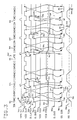
- Fig. 1 shows a circuit 100 for recovering digital data from a magnetic disk or other source.
- the overall function of circuit 100 is to convert a serial analog DATA IN signal on line 101 to a digital DATA OUT signal on line 103.
- FIG. 3 shows timing waveforms 300 associated with the circuit.
- Conventional pulse shaper 110 thresholds signals 101 to produce a waveform 310 having constant-width pulses 311. These pulses, however, may be early or late with respect to the center of a nominal data window or time interval 301.
- the legends in the intervals note whether the pulse is early, late, on time, or missing altogether in each window. (The particular code used in this example disallows pulses in immediately adjacent windows.)
- a voltage-controlled oscillator (VCO) 120 produces a clock waveform 320 on line 121, and an inverted replica on line 121 ⁇ .
- One cycle of wave 320 defines a window interval 301, and one of the transitions 321 defines its midpoint or on-time position.
- Control circuit 122 increases the frequency, and thus advances the phase, of square-wave oscillator 123 upon a signal from AND gate 124, and decreases its frequency, and thus retards the phase, in response to a signal from AND 125.
- VCOs such as 120 are also known as phase-locked oscillators.
- Data latch 130 is set by data pulses 311 on line 103, as shown at transition 331 in waveform 330. Latch 130 is then reset at 332 by the next end-of-window transition 322 in VCO clock 320. Thus, the length of a data-latch pulse 333 varies according to the position of data pulse 311 within window 301.
- Pulse generator 140 contains a single-shot 141 whose output 340 on line 142 contains pulses 341 whose position must track the position of data pulse 311, but whose width must remain as close as possible to that of one half cycle 323 of VCO clock 320. Maintaining this accurate duration, in spite of the inability to compare pulse transitions directly, is a primary object of the present invention.
- line 103 triggers single-shot 141, and the duration of pulse 341 is set by control circuit 143.
- NOR gate 144 increases the pulse duration, while an input on line 142 tends to decrease it.
- Fig. 2 shows an example of a conventional control circuit 200 which can be employed as circuits 122 and 143, Fig. 1.
- Charge pump 210 pushes charge into line 211 at a constant rate in response to a digital signal on "increase” line 212, and pulls charge out of line 211 in response to a signal on "decrease” line 213. This action increases and decreases the voltage of capacitor 220.
- Converter 230 changes the capacitor voltage to a current on output line 231.
- Buffer amplifier 232 presents a high impedance to avoid droop in the capacitor voltage, and resistor 233 converts the buffer output voltage to a current for controlling an external circuit.
- the parameters of circuit 200 can be set so that output 231 changes at any desired rate in response to changes in the input.
- both inputs 212 and 213 may be active at different times during a single cycle without producing large percentage changes in the circuit being controlled.
- the correction time is set so that many hundreds of cycles of signal 340 pass for any major change in the output current (about one disk revolution in the preferred environment).
- Control circuit 122 is set to react much more quickly, almost window-by-window.
- Circuit 122 may also include a resistor (not shown) in series with capacitor 220 to ensure overall stability of its loop.
- delay unit 150 delays data pulses from latch 130 for one window time, in order to differentiate between those windows having a late data pulse, and those having no pulse at all.
- Latch 151 is set by the output of data latch 130 on line 131, and is reset by the following positive transition on inverted VCO clock 121 ⁇ .
- Latch 152 is then set by the output of latch 151, and is reset by the opposite phase of the VCO clock, on line 121. This effectively forms a shift register for delaying data pulses 333 by one window time.
- the output data pulses on line 153 (and the inverse pulses on line 153 ⁇ ) are also lengthened and standardized to fill the entire window interval, whereas the data-latch pulses on line 131 are shorter and of variable width.
- Conventional data decoder 160 converts the delayed data pulses to parallel bits on lines 102, by sensing the state of line 153 when VCO clock line 121 makes a positive transition, and accumulating the bits.
- VCO 120 tracks the data pulses so as to maintain pulses 311 in the center of windows 301 in spite of variations in their overall speed and phase.
- AND 124 tends to increase the frequency of clock 320 during that part of a cycle when a data-latch signal 330 is high and single-shot signal 340 is low.
- AND 125 tends to decrease the clock frequency during that part of a cycle when the opposite condition obtains.
- Waveform 350 illustrates the correction signals on inputs 212 and 213 (for clarity, a positive pulse indicates a pulse at input 212, while a negative pulse in wave 350 indicates a pulse at input 213).
- Waveform 360 illustrates, to a greatly exaggerated scale, the resulting correction signal from output 231.
- Dashed line 369 indicates a nominal baseline value.
- data pulse 311 is on time, so pulses 333 and 341 exactly coincide, and no correction occurs.
- the window designated 302 shows an early data pulse and its resulting correction 351. This increases the frequency of clock 320 very slightly at 361.
- Window 303 has a late data pulse, which generates an opposite correction 352, and decreases the VCO clock frequency very slightly at 362.
- windows such as 304 where no data pulse is present no correction occurs, because neither latch 130 nor pulse generator 140 is triggered by line 103.
- Windows 305 and 306 illustrate the effects of errors in the pulse width of single-shot 141. Because the single-shot pulse in window 305 is longer than the VCO clock pulse, the overhang portion 342 produces a spurious correction pulse 353, incorrectly changing the VCO frequency at 363, even though the data pulse is exactly on time. The opposite effect occurs in window 306; the missing portion 343 of the single-shot pulse causes a false correction at 354 and an improper frequency change at 364.
- control circuit 143 adjusts the width of the single-shot pulses in response to the width of the VCO clock pulses, even though they do not occur at the same time.
- Waveform 370 shows the output data signal on line 153; the signal on line 153 ⁇ is the inverse of this wave.
- Waveform 380 shows the output 211 of control 143, while waveform 390 shows, at a greatly exaggerated scale, the output 231 for controlling the pulse width of single-shot 141; dashed line 399 shows a nominal baseline for the normal width of pulses 341.
- the single-shot output 142 itself returns to the "decrease" input of control 143.
- control 143 produces a correction 381 tending to shorten the width of the pulses 341 via level change 391 (increasing Iout shorter the pulse).
- the "negative" input of control 143 produces a correction 382 tending to lengthen the width of pulses 341 when both data line 153 ⁇ is down (i.e., when 153 is up) at 371 and inverse VCO clock 121 ⁇ is down (check these polarities! One of them seems to be wrong).
- This correction appears as a level change at 392. No changes occur for windows which have no data pulses (note that the corrections occur partially in the window following the data pulse).
- the corrections hover around the nominal baseline value 399 as long as the single-shot pulses 341 have the correct width.
- the time-constant parameters of control 143 are set so that a large number -- several hundred in the preferred embodiment -- of windows are required to alter the pulse width 341 by a significant amount. Thus, the short-term variations about the nominal value have no net effect in windows 301-304.
- the positive correction 383 exceeds the negative correction 384, and the signal 390 trends upward as indicated at 393. This tends to shorten the single-shot pulse width. Conversely, a short pulse causes the positive correction 385 to be shorter than the negative correction 386, causing the signal 390 to trend back downward at 394. This tends to lengthen the single-shot pulse width.
- the undesirable factors affecting the width of the single-shot pulses are environmental, drifting slowly over intervals of minutes. Therefore, the corrections can be made slowly as well. At typical data rates, the width of the single-shot pulses can be corrected in milliseconds. Thus, this circuit can eliminate inaccuracies from environmental and long-term component drifts without any manual adjustments whatever.
Landscapes
- Physics & Mathematics (AREA)
- Nonlinear Science (AREA)
- Stabilization Of Oscillater, Synchronisation, Frequency Synthesizers (AREA)
- Signal Processing For Digital Recording And Reproducing (AREA)
Abstract
Description
- The present invention relates to electronic circuits, and more particularly concerns a circuit for controlling the width of a signal pulse by an oscillator whose frequency and/or phase is controlled by an external signal.
- Controlled oscillators, such as voltage-controlled oscillators and phase-locked oscillators, are frequently used to track the frequency and phase of signals in applications such as digital data recovery, display-scan generation, instrumentation, communications, and diverse other technological areas. The present embodiment was developed in connection with a data-read circuit for a magnetic disk.
- Some applications in the above areas require generation of a pulse whose width must be proportioned closely to that of another signal, even though the two signals may occur at different times in a cycle of the oscillator signal. In the past, the width of the generated pulse has been manually set during manufacture or during service to a fixed nominal width, and then left constant. This requires that each and every unit be adjusted separately, and it makes no provision for changes during operation from variations in temperature, supply voltages, and many other factors. In the unit for which this circuit was developed, a mere 3% error in the pulse width can increase the data error rate by a factor of ten. The effects of mismatching will be explained in more detail in connection with the description of the preferred embodiment.
- The present invention matches the width of a generated pulse to the width of another pulse, even though the latter pulse may occur at a different time, uncorrelated with the occurrence of the generated pulse. The widths are locked together automatically, in spite of environmental variations and other effects. Moreover, the pulse generator needs only to be set to a nominal width approximating its correct width, so that no adjustment of individual circuits is necessary.
- Broadly speaking, a circuit according to the invention accomplishes these and other goals with a controlled oscillator (VCO) for producing clock pulses defining windows for a sequence of input pulses, a data latch for producing timed data pulses from the input pulses, a delay for shifting and standardizing the data pulses, and a pulse generator for producing control pulses whose width tracks that of the clock pulses. The pulse generator includes control means for altering the pulse width of a single-shot in response to a combination of the delayed data pulses, the clock pulses, and the control pulses themselves.
- Fig. 1 is a diagram of a circuit according to the present invention.
- Fig. 2 shows details of a conventional control circuit used in the circuit of Fig. 1.
- Fig. 3 is a timing diagram for the circuit of Fig. 1.
- Fig. 1 shows a
circuit 100 for recovering digital data from a magnetic disk or other source. The overall function ofcircuit 100 is to convert a serial analog DATA IN signal online 101 to a digital DATA OUT signal online 103. FIG. 3 showstiming waveforms 300 associated with the circuit. -
Conventional pulse shaper 110thresholds signals 101 to produce awaveform 310 having constant-width pulses 311. These pulses, however, may be early or late with respect to the center of a nominal data window ortime interval 301. The legends in the intervals note whether the pulse is early, late, on time, or missing altogether in each window. (The particular code used in this example disallows pulses in immediately adjacent windows.) - A voltage-controlled oscillator (VCO) 120 produces a
clock waveform 320 online 121, and an inverted replica on line 121ʹ. One cycle ofwave 320 defines awindow interval 301, and one of thetransitions 321 defines its midpoint or on-time position.Control circuit 122 increases the frequency, and thus advances the phase, of square-wave oscillator 123 upon a signal fromAND gate 124, and decreases its frequency, and thus retards the phase, in response to a signal fromAND 125. VCOs such as 120 are also known as phase-locked oscillators. -
Data latch 130 is set bydata pulses 311 online 103, as shown attransition 331 inwaveform 330. Latch 130 is then reset at 332 by the next end-of-window transition 322 inVCO clock 320. Thus, the length of a data-latch pulse 333 varies according to the position ofdata pulse 311 withinwindow 301. -
Pulse generator 140 contains a single-shot 141 whoseoutput 340 online 142 contains pulses 341 whose position must track the position ofdata pulse 311, but whose width must remain as close as possible to that of one half cycle 323 ofVCO clock 320. Maintaining this accurate duration, in spite of the inability to compare pulse transitions directly, is a primary object of the present invention. To this purpose,line 103 triggers single-shot 141, and the duration of pulse 341 is set bycontrol circuit 143. NORgate 144 increases the pulse duration, while an input online 142 tends to decrease it. - Fig. 2 shows an example of a
conventional control circuit 200 which can be employed ascircuits Charge pump 210 pushes charge intoline 211 at a constant rate in response to a digital signal on "increase"line 212, and pulls charge out ofline 211 in response to a signal on "decrease"line 213. This action increases and decreases the voltage ofcapacitor 220. Converter 230 changes the capacitor voltage to a current onoutput line 231. Buffer amplifier 232 presents a high impedance to avoid droop in the capacitor voltage, andresistor 233 converts the buffer output voltage to a current for controlling an external circuit. The parameters ofcircuit 200 can be set so thatoutput 231 changes at any desired rate in response to changes in the input. Normally, this rate is sufficiently low thatoutput 231 does not change any appreciable amount over a single cycle of the controlled waveform. Thus, bothinputs control circuit 143, the correction time is set so that many hundreds of cycles ofsignal 340 pass for any major change in the output current (about one disk revolution in the preferred environment).Control circuit 122 is set to react much more quickly, almost window-by-window.Circuit 122 may also include a resistor (not shown) in series withcapacitor 220 to ensure overall stability of its loop. - Returning to Figs. 1 and 3, delay
unit 150 delays data pulses fromlatch 130 for one window time, in order to differentiate between those windows having a late data pulse, and those having no pulse at all. Latch 151 is set by the output ofdata latch 130 online 131, and is reset by the following positive transition on inverted VCO clock 121ʹ. Latch 152 is then set by the output of latch 151, and is reset by the opposite phase of the VCO clock, online 121. This effectively forms a shift register for delayingdata pulses 333 by one window time. The output data pulses on line 153 (and the inverse pulses on line 153ʹ) are also lengthened and standardized to fill the entire window interval, whereas the data-latch pulses online 131 are shorter and of variable width. -
Conventional data decoder 160 converts the delayed data pulses to parallel bits onlines 102, by sensing the state ofline 153 whenVCO clock line 121 makes a positive transition, and accumulating the bits. - VCO 120 tracks the data pulses so as to maintain
pulses 311 in the center ofwindows 301 in spite of variations in their overall speed and phase. AND 124 tends to increase the frequency ofclock 320 during that part of a cycle when a data-latch signal 330 is high and single-shot signal 340 is low. AND 125 tends to decrease the clock frequency during that part of a cycle when the opposite condition obtains. - Waveform 350 illustrates the correction signals on
inputs 212 and 213 (for clarity, a positive pulse indicates a pulse atinput 212, while a negative pulse in wave 350 indicates a pulse at input 213).Waveform 360 illustrates, to a greatly exaggerated scale, the resulting correction signal fromoutput 231. Dashedline 369 indicates a nominal baseline value. Duringwindow 301,data pulse 311 is on time, sopulses 333 and 341 exactly coincide, and no correction occurs. The window designated 302 shows an early data pulse and its resultingcorrection 351. This increases the frequency ofclock 320 very slightly at 361. Window 303 has a late data pulse, which generates anopposite correction 352, and decreases the VCO clock frequency very slightly at 362. During windows such as 304 where no data pulse is present, no correction occurs, because neitherlatch 130 norpulse generator 140 is triggered byline 103. - Windows 305 and 306 illustrate the effects of errors in the pulse width of single-
shot 141. Because the single-shot pulse inwindow 305 is longer than the VCO clock pulse, theoverhang portion 342 produces aspurious correction pulse 353, incorrectly changing the VCO frequency at 363, even though the data pulse is exactly on time. The opposite effect occurs inwindow 306; themissing portion 343 of the single-shot pulse causes a false correction at 354 and an improper frequency change at 364. - To eliminate this problem,
control circuit 143 adjusts the width of the single-shot pulses in response to the width of the VCO clock pulses, even though they do not occur at the same time. Waveform 370 shows the output data signal online 153; the signal on line 153ʹ is the inverse of this wave. Waveform 380 shows theoutput 211 ofcontrol 143, while waveform 390 shows, at a greatly exaggerated scale, theoutput 231 for controlling the pulse width of single-shot 141; dashedline 399 shows a nominal baseline for the normal width of pulses 341. First, the single-shot output 142 itself returns to the "decrease" input ofcontrol 143. This produces acorrection 381 tending to shorten the width of the pulses 341 via level change 391 (increasing Iout shorter the pulse). The "negative" input ofcontrol 143 produces acorrection 382 tending to lengthen the width of pulses 341 when both data line 153ʹ is down (i.e., when 153 is up) at 371 and inverse VCO clock 121ʹ is down (check these polarities! One of them seems to be wrong). This correction appears as a level change at 392. No changes occur for windows which have no data pulses (note that the corrections occur partially in the window following the data pulse). The corrections hover around thenominal baseline value 399 as long as the single-shot pulses 341 have the correct width. The time-constant parameters ofcontrol 143 are set so that a large number -- several hundred in the preferred embodiment -- of windows are required to alter the pulse width 341 by a significant amount. Thus, the short-term variations about the nominal value have no net effect in windows 301-304. - However, when the single-shot pulse width becomes too great, as in
window 305, thepositive correction 383 exceeds thenegative correction 384, and the signal 390 trends upward as indicated at 393. This tends to shorten the single-shot pulse width. Conversely, a short pulse causes thepositive correction 385 to be shorter than thenegative correction 386, causing the signal 390 to trend back downward at 394. This tends to lengthen the single-shot pulse width. The undesirable factors affecting the width of the single-shot pulses are environmental, drifting slowly over intervals of minutes. Therefore, the corrections can be made slowly as well. At typical data rates, the width of the single-shot pulses can be corrected in milliseconds. Thus, this circuit can eliminate inaccuracies from environmental and long-term component drifts without any manual adjustments whatever.
Claims (10)
a controlled oscillator (123) for producing clock pulses defining said windows in response to control pulses and data pulses;
a data latch (130) responsive to said input pulses and to said clock pulses for producing said data pulses;
delay means (150) for shifting said data pulses to a later time;
a pulse generator (140) for producing said control pulses having a duration related to the duration of said clock pulses, said pulse generator including
control means (143) responsive to said delay means, said clock pulses and to said control pulses for producing a correction signal,
a single-shot (141) for producing said control pulses having a width responsive to said correction signal.
generating a sequence of said clock pulses;
initiating a data pulse and said control pulse in response to an input pulse;
generating a first correction signal tending to decrease the width of said control pulse from said control pulse itself;
generating a second correction signal tending to increase the width of said control pulse from a function of said clock pulse and said data pulse.
Applications Claiming Priority (2)
| Application Number | Priority Date | Filing Date | Title |
|---|---|---|---|
| US87392486A | 1986-06-13 | 1986-06-13 | |
| US873924 | 2004-06-22 |
Publications (2)
| Publication Number | Publication Date |
|---|---|
| EP0249060A2 true EP0249060A2 (en) | 1987-12-16 |
| EP0249060A3 EP0249060A3 (en) | 1989-02-08 |
Family
ID=25362612
Family Applications (1)
| Application Number | Title | Priority Date | Filing Date |
|---|---|---|---|
| EP87107231A Ceased EP0249060A3 (en) | 1986-06-13 | 1987-05-19 | Self-adjusting single-shot for phase-locked oscillator |
Country Status (2)
| Country | Link |
|---|---|
| EP (1) | EP0249060A3 (en) |
| JP (1) | JPS62299110A (en) |
Cited By (1)
| Publication number | Priority date | Publication date | Assignee | Title |
|---|---|---|---|---|
| US4829258A (en) * | 1987-09-03 | 1989-05-09 | Intel Corporation | Stabilized phase locked loop |
Family Cites Families (2)
| Publication number | Priority date | Publication date | Assignee | Title |
|---|---|---|---|---|
| US4277697A (en) * | 1979-01-15 | 1981-07-07 | Norlin Industries, Inc. | Duty cycle control apparatus |
| DE3115057C2 (en) * | 1981-04-14 | 1984-03-29 | Siemens AG, 1000 Berlin und 8000 München | Phase locked loop with a digital phase discriminator |
-
1987
- 1987-05-08 JP JP62110903A patent/JPS62299110A/en active Pending
- 1987-05-19 EP EP87107231A patent/EP0249060A3/en not_active Ceased
Cited By (3)
| Publication number | Priority date | Publication date | Assignee | Title |
|---|---|---|---|---|
| US4829258A (en) * | 1987-09-03 | 1989-05-09 | Intel Corporation | Stabilized phase locked loop |
| GB2209443A (en) * | 1987-09-03 | 1989-05-10 | Intel Corp | Stabilized phase locked loop |
| GB2209443B (en) * | 1987-09-03 | 1992-01-15 | Intel Corp | Stabilized phase locked loop |
Also Published As
| Publication number | Publication date |
|---|---|
| JPS62299110A (en) | 1987-12-26 |
| EP0249060A3 (en) | 1989-02-08 |
Similar Documents
| Publication | Publication Date | Title |
|---|---|---|
| JP2771928B2 (en) | Phase locked loop circuit | |
| US4922141A (en) | Phase-locked loop delay line | |
| EP0091200B1 (en) | Clock recovery apparatus | |
| US7349513B2 (en) | Process, voltage, temperature independent switched delay compensation scheme | |
| JPS63146613A (en) | Delay circuit | |
| US5008629A (en) | Frequency synthesizer | |
| EP0657796A2 (en) | A clock generator and phase comparator for use in such a clock generator | |
| US6005425A (en) | PLL using pulse width detection for frequency and phase error correction | |
| US6066988A (en) | Phase locked loop circuit with high stability having a reset signal generating circuit | |
| GB1526711A (en) | Clock regenerator circuit arrangement | |
| US6496554B1 (en) | Phase lock detection circuit for phase-locked loop circuit | |
| JPH02257718A (en) | Digital phase lochloop | |
| US6445229B1 (en) | Digital phase lock loop | |
| US4774479A (en) | Phase locked loop circuit | |
| US6897691B2 (en) | Phase locked loop with low steady state phase errors and calibration circuit for the same | |
| US5343167A (en) | One-shot control circuit for tracking a voltage-controlled oscillator | |
| US7375592B2 (en) | System and method for maintaining an accurate frequency on a voltage controlled oscillator | |
| US4034309A (en) | Apparatus and method for phase synchronization | |
| EP0164785A1 (en) | Electric circuit arrangement comprising a phase control-circuit | |
| EP0741931A1 (en) | Phase-locked loop, phase comparator for use in the phase-locked loop, and reproducing device including the phase-locked loop | |
| EP0625826B1 (en) | Programmable frequency divider in a phase lock loop | |
| EP0249060A2 (en) | Self-adjusting single-shot for phase-locked oscillator | |
| US6115439A (en) | Free running digital phase lock loop | |
| JP2811994B2 (en) | Phase locked loop | |
| JPH0250655B2 (en) |
Legal Events
| Date | Code | Title | Description |
|---|---|---|---|
| PUAI | Public reference made under article 153(3) epc to a published international application that has entered the european phase |
Free format text: ORIGINAL CODE: 0009012 |
|
| AK | Designated contracting states |
Kind code of ref document: A2 Designated state(s): DE FR GB |
|
| 17P | Request for examination filed |
Effective date: 19880426 |
|
| PUAL | Search report despatched |
Free format text: ORIGINAL CODE: 0009013 |
|
| AK | Designated contracting states |
Kind code of ref document: A3 Designated state(s): DE FR GB |
|
| 17Q | First examination report despatched |
Effective date: 19910225 |
|
| STAA | Information on the status of an ep patent application or granted ep patent |
Free format text: STATUS: THE APPLICATION HAS BEEN REFUSED |
|
| 18R | Application refused |
Effective date: 19921026 |
|
| RIN1 | Information on inventor provided before grant (corrected) |
Inventor name: SWART, DAVID PETER Inventor name: RAE; JAMES WILSON |