EP0248513A2 - Method for routing - Google Patents
Method for routing Download PDFInfo
- Publication number
- EP0248513A2 EP0248513A2 EP87303026A EP87303026A EP0248513A2 EP 0248513 A2 EP0248513 A2 EP 0248513A2 EP 87303026 A EP87303026 A EP 87303026A EP 87303026 A EP87303026 A EP 87303026A EP 0248513 A2 EP0248513 A2 EP 0248513A2
- Authority
- EP
- European Patent Office
- Prior art keywords
- cell
- cost
- cells
- flags
- further characterized
- Prior art date
- Legal status (The legal status is an assumption and is not a legal conclusion. Google has not performed a legal analysis and makes no representation as to the accuracy of the status listed.)
- Granted
Links
Images


Classifications
-
- G—PHYSICS
- G06—COMPUTING; CALCULATING OR COUNTING
- G06F—ELECTRIC DIGITAL DATA PROCESSING
- G06F30/00—Computer-aided design [CAD]
- G06F30/30—Circuit design
- G06F30/39—Circuit design at the physical level
- G06F30/394—Routing
Definitions
- This invention relates to a routing method suitable for generating routes for implementing efficient interconnection of integrated circuit packages in a multilayer circuit board.
- circuit board design method there are two primary steps: deciding where integrated circuit packages will be placed and deciding where conductors should be routed to interconnect the packages.
- This invention is concerned with routing conductors after the package positions have been set.
- Element - one of a number of items having a specific shape, size and XYZ position which are to be selectively interconnected.
- Signal - elements have the same signal if they are, or must be, connected.
- Sumnet - elements have the same sumnet if they are connected.
- Route - a series of contiguous linear elements of specific length, orientation, and position which together define a path between two elements.
- a classical algorithm used for deriving interconnection routes for printed circuit boards is the Lee algorithm. While adequate for simple structures where the number of disconnections is low, the Lee algorithm requires an inordinate amount of memory if used for multi-chip circuit boards where there might be of the order of 4,000 disconnections.
- a method of deriving interconnection routes between elements in a connection medium comprising the steps of:
- the cells can be rectangular cells derived by notionally dividing the board area.
- Said cell addresses can further include a layer level. Preferably such cells are of identical size.
- Said pointer directions can comprise compass directions north, south, east, west, northeast, northwest, southeast, southwest, up and down, the compass pointer directions representing directions to eight four-sided square cells which exist around a four-sided cell, and the up and down pointer directions representing directions from one map layer respectively to an overlying and an underlying map layer.
- Other flags stored within the cell map can be used to show why a cell is full. Such flags can show vias to an overlying or underlying board layer, or board edge cells, conductors or elements, and target and seed cells.
- each of the cells within the cell memory map has associated therewith an address, a permanent store within which is stored data representing the condition of the cell in the completed map, and a temporary store representing a temporary condition within the cell during operation of a flooding routine comprising steps (vii) to (xiii).
- the method can further utilize a road map indicative of cell addresses where certain route orientations are not permitted, the method comprising inspecting said road map after each cell selection to show rapidly in which orientations routes are permitted.
- the shortest routes for interconnecting integrated circuit packages 10 are routes extending directly between the IC package pins 12.
- this arrangement gives rise to many overlapping routes. This is untenable since overlapping routes can only be electrically separated by employing a large number of circuit board layers insulated from one another.
- Shown in Figure 2 is a typical practical route between points M and N at the top layer of a four-layer board.
- the route includes two short diagonal segments 24 and an east-west segment 26 on a top board layer 14, two vias 27 to a lower board layer 16 and a north-south segment 28 on the lower layer.
- This route uses predominantly east-west and north-south sections. Additionally, the east-west route sections are located predominantly in board layers where there are few north-south route sections and vice versa to obtain high route density.
- input data for a routing method consists of board data and element data.
- the board data defines the board dimensions, number of board layers, a grid size, and the technology.
- the grid size data determines how the interconnection medium is to be notionally divided into cells, and the technology file sets certain constraints, for example, on the thickness of routes and their mutual spacing.
- the element data defines the shape, size and position of elements, and the signals and sumnets of these elements. Effectively, the element data lists a set of disconnections.
- the board and element data are fed to a controller which subjects data to a known minimum spanning tree (MST) algorithm to determine the minimum length of direct spans required to connect elements of the same signal.
- MST minimum spanning tree
- the MST algorithm selects a list of interconnections from the list of disconnections.
- the interconnections are ranked in the order in which routes are to be derived, i.e. the work order.
- a flooding routine is used to derive a route for each of the interconnections in turn.
- the output of the router is data representing a list of line segments having length, position and orientation. This output data is used to implement the routes as copper lines and vias on a printed circuit board.
- board data is recorded in the form of a cell memory map.
- the area of the multilayer board is notionally divided into a maximum of 220 rectangular cells in an XY grid, data being stored at each of a corresponding number of cell addresses.
- the board is divided vertically into a number of layers so the cell addresses also include a Z component.
- any three elements A1, A2 and A3 having the same signal but different sumnet can be connected by disconnections A1A2 and A2A3 or A1A3 and A1A2, or A1A3 and A3A2.
- each element is analyzed to define the boundary of a rectangle into which it fits. The center of the rectangle is given XY coordinates as are all other rectangles derived from elements of the same signal.
- the interconnections for those common signal elements are then listed starting with the minimum length required to effect an interconnection between two centers, then the next longest, etcetera until all elements of the same signal would, if the interconnections were actually made, have the same sumnet.
- a list corresponding to the order in which routes are to be derived is then derived from the unordered MST list.
- Sorting of interconnections may be based on any one of a number of known ordering schemes and multiple passes through a flooding routine described subsequently may utilize different ones of the ordering schemes. During at least one pass through the ordering routine, the order for assigning routes depends on a set of MAOMIC (maximum occupancy minimum capacity) factors.
- MAOMIC maximum occupancy minimum capacity
- the board and element data is first mapped onto the memory map.
- the memory map At each cell within the memory map, there is a permanent and a temporary storage location.
- each of the cells is given one of the flags 00 to 15 which are listed below together with their binary coded decimal equivalents.
- a MAOMIC factor is derived for every vertical and horizontal grid line.
- Each interconnection is then labelled with the highest MAOMIC product of all the grid lines which it crosses.
- the MAOMIC factors are AB : 1.6, GH : 1.4, EF : 1.3 and CD : 1.0.
- the work to be done is then listed in decreasing MAOMIC factor order.
- the grid spacing is the same as the permitted conductor route spacing to facilitate derivation of the MAOMIC factors.
- the circuit board of Figure 5 is simplified in that it is two-dimensional, consisting of a single board layer. However, the MAOMIC factor can be readily derived for grids of a three-dimensional interconnection medium.
- the MAOMIC routine results in a work order list of pairs of elements requiring interconnection.
- the cell data is crystallized.
- a cell is selected within each element to be the seed cells (05).
- the other cells of the element i.e. those having the same signal and sumnet are considered.
- Each of the cells is related to the element seed by a system of backpointers (06 to 15), the pointers being north, south, east, west, northwest, northeast, southwest, southeast, up (for a cell in an underlying board layer) and down (for a cell in an overlying board layer).
- a seed cell shown as S is located at position (6,6).
- the cells around (6,6) have pointer directions corresponding to the cardinal and half-cardinal points.
- Back pointer directions for the next outer layer of cells within the element are assigned by successively considering the inner cells as temporary seeds and so on until backpointers have been allocated to all of the elements in the MAOMIC listing.
- each of the listed pairs of elements are considered in turn.
- the smaller element is selected as a source area and the other as a target area ( Figure 8).
- the backpointer data of the target cells is deleted and is replaced by target (03) encoding.
- each cell has in its permanent store a flag which indicates whether the cell is full (01 to 15) or available for flooding (00) and if it is full, the reason why. A full cell is not available for interconnection routing.
- the possible flags with binary coded flag data are as shown previously.
- the length of moving from one cell to another is the length of a single cell.
- the copper routes on any one layer extend predominantly in one direction to obtain maximum packing density.
- copper routes may be predominantly north-south and in an underlying layer predominantly east-west. So that the layer routing preference can be taken account of in the flooding routine, the north and south pointer directions are given a lower cost than the east and west pointer directions in the top board and vice versa in the lower board layer.
- the half-cardinal directions such as northeast and southwest are registered as more costly and the vertical routes up and down are registered as the most costly. The cost of the routes is selected for a particular board design.
- a typical pointer cost list is shown below.
- the list corresponds to a four-layer board in which north-south routing is predominant in layers 1 and 3 and east-west routing is predominant in layers 0 and 2.
- a "0" cost means that routing in such a direction is not permitted.
- 28 storage bins are set up for storing cell addresses corresponding to a particular route cost, i.e. the cost of moving to a cell from a source seed cell.
- a route cost i.e. the cost of moving to a cell from a source seed cell.
- the addresses of all cells of the source are first stacked into a cost 0 bin.
- the cost of a route from the source seed to another cell in the source is 0 since the source is a single set of interconnected full cells representing a single conducting entity. As a move is made into a cell which is not the source, however, the cost is increased from 0.
- a cell address is selected from the lowest cost bin containing cell addresses, for example, the bin of cost A.
- a cell is selected from a bin, its address and backpointer direction are transferred to the temporary store in the memory map. Cells adjacent to the selected cell are inspected. If an inspected cell is not full, then its address and the pointer direction back to the selected cell are stored in the cost (A + X) bin where X is the cost of moving from the selected cell to the cell being inspected. The remaining empty cells around the selected cell are then inspected in turn. The same procedure is adopted for the remaining cells in the cost A bin. Initially the cells are selected from the cost 0 bin since this is occupied by the source cells. When the cost 0 bin is empty, cells are selected from the cost 1 bin and so on.
- the address of that particular cell address may appear in a number of the bins. However, once a cell has been selected and entered in the temporary store of the memory map, the address of the cell is discarded from any higher order storage bins.
- a target (03) cell is reached as a result of the inspection process.
- the flooding routine is however continued until a target cell has been selected from its cost bin and transferred to the memory map. Since the data related to each cell visited in the flooding routine includes a backpointer direction, the cell data is, in effect, stored in association with the data of the next cell into which flooding takes place. Thus when a target cell is reached, the path through the flooded cells by which the target cell was reached can be traced back to the source.
- the routing procedure goes through ionization and recrystallization routines.
- the target (03) flags in the temporary storage locations of the target cells are replaced by copper flags (04).
- the recrystallization routine pointer directions are assigned to the target cells relative to the source seed and these backpointer directions are assigned to the permanent store.
- the pair of interconnected elements form, in effect, a single new element.
- the list of interconnections is immediately edited by destroying the target sumnet within the list of work to be done and replacing the interconnected elements by the new element.
- the flooding routine is repeated to effect routes for each of the interconnections in order.
- the result stored is a list of contiguous linear route segments having length, position and orientation.
- the list of linear segments can be readily used in the manufacture of integrated circuit boards.
- Structure 1 must be connected to structure 3 since it has the same signal but a different subnet. Structure 2 is and must remain disconnected.
- Structure 1 is seeded at (2,4)
- Structure 2 is seeded at (5,4)
- Structure 3 is seeded at (7,5)
- Blank cells are empty (00)
- the temporary storage at (2,4) is checked for empty; it is.
- the backpointer (seed) is written in temporary storage. Then the visit of the eight neighbouring cells begins; Going North first, the cell at (2,3) is examined.
- the cell at (3,4) temporary store is empty. Visit neighbours.
- Extract next cell from the least cost non-empty bin (1) (1,4) East having base cost 1. Cell at (1,4) temporary is empty.
- Extract cell from the least cost non-empty bin (1) (4,4) West, base cost 1; cell at (4,4) temporary is empty.
- Extract cell from the least cost, non-empty bin (3) (2,3) South, base cost 3; cell at (2,3) temporary is empty.
- the last three addresses are extracted from the least cost bin (3) and their neighbours are visited.
- the first four cells are then extracted from least cost bin (4) and their neighbours are visited.
- the flooding progresses until cell (6,3) W is extracted from the least cost bin (6). It was put there by the eastward visit from cell (5,3) in cost bin 5. From (6,3) when visiting the eastward neighbour at (7,3), the temporary storage is found to contain T (target 03). The algorithm considers (7,3) to be empty and stores (7,3) W in cost bin 7. The algorithm progresses as usual.
- the traceback routine starts from (7,3) and follows the backpointers in sequence.
- the permanent storage structures are then adjusted as shown.
- the temporary storage is cleared of the expansion data and reset to model the contents of the permanent storage. All bins are cleared of address and backpointer data. The cell map and bins are ready for another exercise of the flooding algorithm.
- this flooding routine provides an effective compromise between route efficiency and low memory requirement.
- DIP dual in-line package
- corresponding pins of adjacent DIPs are often interconnected.
- a grid of 0.020 spacing has a standard conductor spacing of 20 cells and a circular pin solder area of diameter 50 cells. This leaves room for only 2 conductors in a 100 grid spacing. To most effectively use the space around pins for routing, all route assignments are made subject to a road map which forces some routing discipline over the flooding algorithm.
- the road map shown in Figure 30 is used during the flooding process.
- a cell is extracted from the least cost non-empty bin, its position on the road map is identified.
- a cell C at (0.N40, 0.M60) is identified in Figure 31.
- the road map is used to control the neighbour positioning process. In the case of C, visits are restricted to NW, W, SW, SE and E thus preventing undesirable flooding towards N, NE and S.
- the previous example is completed as shown in Figure 31 where broken lines are tracks on a lower layer and a via is present at location A.
- the road map keeps the flooding algorithm from grid lines 0.020 and 0.080 thus providing a better utilization of the space where vias must be positioned.
- a secondary effect of the road map is substantially to reduce the amount of computer time and computer storage required to run the flooding algorithm. Time is saved by preventing undesirable visits and space is saved, by saving on bin storage.
- a different technology file may have different package pin size, shape and spacing and a different grid size.
- limits are set to the vertical travel between board layers by specifying, for example, only two vias in any interconnect route.
- an initial pass is made through the work order to assign only the most efficient straight and "L" shaped routes at a single board layer to those interconnections susceptible of such routing.
- more complex routes which may extend to multiple layers are assigned.
- a ceiling can be placed on the cost of any route.
- the route, its cost, etcetera is checked against a limitation indicator.
- a particular margin is set.
- the margin is the extent to which a larger rectangle extends beyond the minimum area rectangle. If a small margin is set then the interconnections must be within or very close to the minimum area rectangle.
- connection method is described in the context of a multilayer printed circuit board, it will be appreciated that the connection method has a more universal application.
- the MAOMIC and flooding routines can be performed by suitably programming a computer, the computer having a memory for storing the memory map, the temporary and permanent results of running the flooding routine, the cost bins and their contents, the road map limitations etcetera.
Abstract
Description
- This invention relates to a routing method suitable for generating routes for implementing efficient interconnection of integrated circuit packages in a multilayer circuit board.
- In a circuit board design method there are two primary steps: deciding where integrated circuit packages will be placed and deciding where conductors should be routed to interconnect the packages. This invention is concerned with routing conductors after the package positions have been set.
- In the specification, the following definitions apply.
- Element - one of a number of items having a specific shape, size and XYZ position which are to be selectively interconnected.
- Signal - elements have the same signal if they are, or must be, connected.
- Sumnet - elements have the same sumnet if they are connected.
- Disconnections - if two elements have the same signal but different sumnets then a disconnection exists between them.
- Interconnections - that selection from the disconnections obtained by applying the "minimum spanning tree" (MST) algorithm; also called "work to be done".
- Route - a series of contiguous linear elements of specific length, orientation, and position which together define a path between two elements.
- Cell - a sub-division of the interconnection medium.
- A classical algorithm used for deriving interconnection routes for printed circuit boards is the Lee algorithm. While adequate for simple structures where the number of disconnections is low, the Lee algorithm requires an inordinate amount of memory if used for multi-chip circuit boards where there might be of the order of 4,000 disconnections.
- According to one aspect of the invention, there is provided a method of deriving interconnection routes between elements in a connection medium comprising the steps of:
- i) generating a cell map consisting of a number of addressable cells representing grid positions in the connection medium;
- ii) storing a plurality of pointer directions according to permissible route segment orientations, each of the pointer directions having an associated cost;
- iii) setting up a series of cost bins from at least cost bin upwards, each bin for storing data items having a cell address and an associated pointer direction;
- iv) for a list of interconnections, designating certain of the addressable cells which can accommodate routes as empty and designating other cells which cannot accommodate routes as full;
- v) selecting an interconnection having source and target elements each made up of a number of connected cells;
- vi) assigning the source cell addresses to a 0 cost bin;
- vii) selecting a cell from the least cost (n) bin containing cell addresses and entering its pointer direction in the corresponding address of the cell map;
- viii) considering cells immediately adjacent to the selected cell;
- ix) assessing a backpointer direction for each considered cell, being a direction back to the selected cell from the considered cell;
- x) if the considered cell is in the source element placing the cell address in the cost n bin and if the considered cell is empty and has a pointer direction of cost m, placing the cell address in the cost (n + m) bin;
- xi) repeating the steps (vii) to (x) for each cell listed in the cost n bin;
- xii) repeating the step (xi) for progressively higher cost bins until a target cell is selected;
- xiii) retracing backpointers from the target cell to the source;
- xiv) recording the route of said retraced pointers;
- xv) repeating steps (v) to (xiv) for other interconnections.
- The cells can be rectangular cells derived by notionally dividing the board area. Said cell addresses can further include a layer level. Preferably such cells are of identical size.
- Said pointer directions can comprise compass directions north, south, east, west, northeast, northwest, southeast, southwest, up and down, the compass pointer directions representing directions to eight four-sided square cells which exist around a four-sided cell, and the up and down pointer directions representing directions from one map layer respectively to an overlying and an underlying map layer. Other flags stored within the cell map can be used to show why a cell is full. Such flags can show vias to an overlying or underlying board layer, or board edge cells, conductors or elements, and target and seed cells.
- Preferably each of the cells within the cell memory map has associated therewith an address, a permanent store within which is stored data representing the condition of the cell in the completed map, and a temporary store representing a temporary condition within the cell during operation of a flooding routine comprising steps (vii) to (xiii).
- The method can further utilize a road map indicative of cell addresses where certain route orientations are not permitted, the method comprising inspecting said road map after each cell selection to show rapidly in which orientations routes are permitted.
- An embodiment of the invention will now be described by way of example with reference to the accompanying drawings in which:-
- Figure 1 is a schematic plan view of a printed circuit board showing a number of direct spanning conductor routes between integrated circuit chips;
- Figure 2 shows a grid representation of part of a simple multilayer circuit board showing a single interconnection and its corresponding conductor route;
- Figure 3 is a flow diagram showing operation of a routing method according to the invention;
- Figure 4 shows a grid representation of a group of elements with their respective signal and sumnet data;
- Figures 5 to 8 show grid representations of part of a circuit board showing the occupancy and capacity of several grid lines;
- Figures 9 to 27 show grid representations of part of a circuit board during successive stages in the operation of a flooding algorithm used to derive a route between source and target cells; and
- Figures 28 to 31 show grid representations of part of a circuit board showing operation of a road map feature of the flooding algorithm.
- As shown in Figure 1, the shortest routes for interconnecting
integrated circuit packages 10 are routes extending directly between theIC package pins 12. However, this arrangement gives rise to many overlapping routes. This is untenable since overlapping routes can only be electrically separated by employing a large number of circuit board layers insulated from one another. - Shown in Figure 2 is a typical practical route between points M and N at the top layer of a four-layer board. The route includes two short
diagonal segments 24 and an east-west segment 26 on atop board layer 14, twovias 27 to alower board layer 16 and a north-south segment 28 on the lower layer. This route uses predominantly east-west and north-south sections. Additionally, the east-west route sections are located predominantly in board layers where there are few north-south route sections and vice versa to obtain high route density. - Referring to Figure 3, input data for a routing method consists of board data and element data.
- Typically the board data defines the board dimensions, number of board layers, a grid size, and the technology. The grid size data determines how the interconnection medium is to be notionally divided into cells, and the technology file sets certain constraints, for example, on the thickness of routes and their mutual spacing.
- The element data defines the shape, size and position of elements, and the signals and sumnets of these elements. Effectively, the element data lists a set of disconnections.
- The board and element data are fed to a controller which subjects data to a known minimum spanning tree (MST) algorithm to determine the minimum length of direct spans required to connect elements of the same signal. The MST algorithm selects a list of interconnections from the list of disconnections.
- Subsequently at a MAOMIC ordering section, the interconnections are ranked in the order in which routes are to be derived, i.e. the work order.
- At a flooding section, a flooding routine is used to derive a route for each of the interconnections in turn. The output of the router is data representing a list of line segments having length, position and orientation. This output data is used to implement the routes as copper lines and vias on a printed circuit board.
- Considering the various parts of the method in detail, to initiallize the routing process, board data is recorded in the form of a cell memory map. The area of the multilayer board is notionally divided into a maximum of 2²⁰ rectangular cells in an XY grid, data being stored at each of a corresponding number of cell addresses. The board is divided vertically into a number of layers so the cell addresses also include a Z component.
- As indicated previously a selection of interconnections is made from the disconnections using the MST algorithm. Thus referring to Figure 4, any three elements A₁, A₂ and A₃ having the same signal but different sumnet can be connected by disconnections A₁A₂ and A₂A₃ or A₁A₃ and A₁A₂, or A₁A₃ and A₃A₂. Using the MST algorithm each element is analyzed to define the boundary of a rectangle into which it fits. The center of the rectangle is given XY coordinates as are all other rectangles derived from elements of the same signal. The interconnections for those common signal elements are then listed starting with the minimum length required to effect an interconnection between two centers, then the next longest, etcetera until all elements of the same signal would, if the interconnections were actually made, have the same sumnet.
- As briefly indicated previously, a list corresponding to the order in which routes are to be derived is then derived from the unordered MST list.
- Sorting of interconnections may be based on any one of a number of known ordering schemes and multiple passes through a flooding routine described subsequently may utilize different ones of the ordering schemes. During at least one pass through the ordering routine, the order for assigning routes depends on a set of MAOMIC (maximum occupancy minimum capacity) factors.
- To develop the MAOMIC factors, the board and element data is first mapped onto the memory map. At each cell within the memory map, there is a permanent and a temporary storage location. In a cell encoding process, each of the cells is given one of the
flags 00 to 15 which are listed below together with their binary coded decimal equivalents.
- As a result of the encoding process, certain of the cells are recorded as empty (00) and therefore available for flooding whereas the others are recorded as full (01 to 15).
- With reference to Figure 5, to obtain a MAOMIC factor, the vertical and horizontal grid lines defining cell positions are considered and for each grid line, a capacity assessment (N) is made, Figure 5, this being the number of cells or grid positions along the length of the grid line that are empty and therefore can accommodate a route crossing. As shown in Figure 5, five out of the ten possible horizontal grid lines are full at the vertical x = 6 (N = 5). Then an occupancy assessment (M) is made as to how many connections would, if made to span directly between elements, cross each grid line. As shown in Figure 6, five routes would cross grid line x = 6 if the routes were directly drawn (M = 5). MAOMIC factors, being the products of the occupancy and inverse capacity, are derived for each grid line, the MAOMIC factor of x = 6 being M x 1/N = 1. A MAOMIC factor is derived for every vertical and horizontal grid line. Each interconnection is then labelled with the highest MAOMIC product of all the grid lines which it crosses. Thus, in the five interconnections of Figure 7, the MAOMIC factors are AB : 1.6, GH : 1.4, EF : 1.3 and CD : 1.0. The work to be done is then listed in decreasing MAOMIC factor order. In the embodiment described, the grid spacing is the same as the permitted conductor route spacing to facilitate derivation of the MAOMIC factors. The circuit board of Figure 5 is simplified in that it is two-dimensional, consisting of a single board layer. However, the MAOMIC factor can be readily derived for grids of a three-dimensional interconnection medium.
- The MAOMIC routine results in a work order list of pairs of elements requiring interconnection.
- As part of the cell encoding procedure, the cell data is crystallized. During crystallization and referring to Figure 8, a cell is selected within each element to be the seed cells (05). The other cells of the element i.e. those having the same signal and sumnet are considered. Each of the cells is related to the element seed by a system of backpointers (06 to 15), the pointers being north, south, east, west, northwest, northeast, southwest, southeast, up (for a cell in an underlying board layer) and down (for a cell in an overlying board layer).
- Referring to Figure 8, a seed cell shown as S is located at position (6,6). The cells around (6,6) have pointer directions corresponding to the cardinal and half-cardinal points. Back pointer directions for the next outer layer of cells within the element are assigned by successively considering the inner cells as temporary seeds and so on until backpointers have been allocated to all of the elements in the MAOMIC listing.
- In the flooding routine each of the listed pairs of elements are considered in turn. The smaller element is selected as a source area and the other as a target area (Figure 8). The backpointer data of the target cells is deleted and is replaced by target (03) encoding.
- The principle of the flooding routine is then tentatively to move from the source into surrounding successive fronts of empty cells of the memory map until the target is reached. In the memory map initially derived, each cell has in its permanent store a flag which indicates whether the cell is full (01 to 15) or available for flooding (00) and if it is full, the reason why. A full cell is not available for interconnection routing. The possible flags with binary coded flag data are as shown previously.
- In geometrical terms, the length of moving from one cell to another is the length of a single cell. However in according routes to a particular layer of a circuit board, it is preferred that the copper routes on any one layer extend predominantly in one direction to obtain maximum packing density. Thus typically in a top board layer, copper routes may be predominantly north-south and in an underlying layer predominantly east-west. So that the layer routing preference can be taken account of in the flooding routine, the north and south pointer directions are given a lower cost than the east and west pointer directions in the top board and vice versa in the lower board layer. The half-cardinal directions such as northeast and southwest are registered as more costly and the vertical routes up and down are registered as the most costly. The cost of the routes is selected for a particular board design. A typical pointer cost list is shown below. The list corresponds to a four-layer board in which north-south routing is predominant in
layers layers 
- For operating the flooding routine, 2⁸ storage bins are set up for storing cell addresses corresponding to a particular route cost, i.e. the cost of moving to a cell from a source seed cell. To derive a route, the addresses of all cells of the source are first stacked into a
cost 0 bin. The cost of a route from the source seed to another cell in the source is 0 since the source is a single set of interconnected full cells representing a single conducting entity. As a move is made into a cell which is not the source, however, the cost is increased from 0. - In the flooding routine, a cell address is selected from the lowest cost bin containing cell addresses, for example, the bin of cost A. Whenever a cell is selected from a bin, its address and backpointer direction are transferred to the temporary store in the memory map. Cells adjacent to the selected cell are inspected. If an inspected cell is not full, then its address and the pointer direction back to the selected cell are stored in the cost (A + X) bin where X is the cost of moving from the selected cell to the cell being inspected. The remaining empty cells around the selected cell are then inspected in turn. The same procedure is adopted for the remaining cells in the cost A bin. Initially the cells are selected from the
cost 0 bin since this is occupied by the source cells. When thecost 0 bin is empty, cells are selected from thecost 1 bin and so on. - Because normally there exist several ways to move into a particular cell from cells adjacent to it, the address of that particular cell address may appear in a number of the bins. However, once a cell has been selected and entered in the temporary store of the memory map, the address of the cell is discarded from any higher order storage bins.
- Eventually, after a number of iterations of the flooding routine, a target (03) cell is reached as a result of the inspection process. The flooding routine is however continued until a target cell has been selected from its cost bin and transferred to the memory map. Since the data related to each cell visited in the flooding routine includes a backpointer direction, the cell data is, in effect, stored in association with the data of the next cell into which flooding takes place. Thus when a target cell is reached, the path through the flooded cells by which the target cell was reached can be traced back to the source.
- Following a target strike, the routing procedure goes through ionization and recrystallization routines. In the ionization routine, the target (03) flags in the temporary storage locations of the target cells are replaced by copper flags (04). Then in the recrystallization routine, pointer directions are assigned to the target cells relative to the source seed and these backpointer directions are assigned to the permanent store.
- When a route is derived, then the pair of interconnected elements form, in effect, a single new element. The list of interconnections is immediately edited by destroying the target sumnet within the list of work to be done and replacing the interconnected elements by the new element.
- The flooding routine is repeated to effect routes for each of the interconnections in order. The result stored is a list of contiguous linear route segments having length, position and orientation. The list of linear segments can be readily used in the manufacture of integrated circuit boards.
- A complete example of use of the flooding algorithm including encoding and traceback steps follows with reference to Figures 9 to 27.
- A typical input shown with 6 elements:
A Signal S Subnet N =Structure 1
B Signal R Subnet K =Structure 2
C Signal S Subnet M =Structure 3
D Signal S Subnet M =Structure 3
E Signal S Subnet M =Structure 3
F Signal S Subnet M =Structure 3 -
Structure 1 must be connected to structure 3 since it has the same signal but a different subnet.Structure 2 is and must remain disconnected. - The permanent storage encoding of the cell map:
Structure 1 is seeded at (2,4)
Structure 2 is seeded at (5,4)
Structure 3 is seeded at (7,5) - Blank cells are empty (00)
- The corresponding temporary storage encoding prior to flooding shows:
C = copper = 04
blank = empty = 00
Incremental costs are:
N - S = 3
E - W = 1
half-cardinal directions = 5
- After preparation of the source and the target, the temporary storage contents are as shown.
- 1. The source has been emptied and the cells are in the
cost 0 bin with their proper backpointer (seed) - 2. The target is marked with T = target = 03
- Other structures are left unchanged. Initially, permanent storage will not be modified by the flooding algorithm.

- The first cell from the least cost bin (0) is picked up. This is the (2,4) seed having a base cost = 0.
The temporary storage at (2,4) is checked for empty; it is.
The backpointer (seed) is written in temporary storage.
Then the visit of the eight neighbouring cells begins;
Going North first, the cell at (2,3) is examined. - It is empty; so its address and a backpointer (south) is stored in bin of cost = base cost + increased cost of North, i.e. the (bin for cost = 0 + 3 = 3)

- Next visit the other neighbouring cells

- Extract the next cell from the least cost non-empty bin. This is cell (3,4) in the bin of
cost 0. The cell at (3,4) temporary store is empty. Visit neighbours.
- Extract next cell from the least cost non-empty bin (1) (1,4) East having base cost = 1. Cell at (1,4) temporary is empty.

- Extract cell from the least cost non-empty bin (1) (4,4) West, base cost = 1; cell at (4,4) temporary is empty.

- Extract cell from the least cost, non-empty bin (3) (2,3) South, base cost = 3; cell at (2,3) temporary is empty.
- The visit to neighbouring cells proceeds as before. For brevity purposes, the second appearance of the address of cells in the cost bins is replaced by a dot. The validity of this simplification is explained in
step 13.
- The last three addresses are extracted from the least cost bin (3) and their neighbours are visited.

- The first four cells are then extracted from least cost bin (4) and their neighbours are visited.

- Extract the next address from the least cost non-empty bin (4), (3,3) W, base cost = 4; cell at (3,3) temporary is not empty. This means that that cell already flooded is at a lesser or equal cost and so no visit to it is required.

- The flooding progresses until cell (6,3) W is extracted from the least cost bin (6). It was put there by the eastward visit from cell (5,3) in
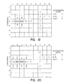
cost bin 5. From (6,3) when visiting the eastward neighbour at (7,3), the temporary storage is found to contain T (target 03). The algorithm considers (7,3) to be empty and stores (7,3) W incost bin 7. The algorithm progresses as usual. - When (7,3) W is extracted from the
least cost bin 7, the temporary storage is found to contain T (target 03). Under these circumstances, the backpointer is stored at (7,3) temporary and the flooding algorithm terminates successfully. The reach cost is 7. The numbers in Figure 20 show the cost bins from which the backpointers are extracted to illustrate the wavefront progression of the flooding algorithm. - The traceback routine starts from (7,3) and follows the backpointers in sequence.
(7,3) W
(6,3)W line 1 from (7,3) to (4,3) = new element G (Fig. 25)
(5,3) W
(4,3)S line 2 from (4,3) to (4,4) = new element H
(4,4) W
(3,4)Seed line 3 from (4,4) to (3,4) = new element I - Considering Figures 9 and 25 the routing results in:

- Subnet M of signal S has disappeared.
- The permanent storage structures are then adjusted as shown.
- The temporary storage is cleared of the expansion data and reset to model the contents of the permanent storage. All bins are cleared of address and backpointer data. The cell map and bins are ready for another exercise of the flooding algorithm.
- In combination with the MAOMIC ordering scheme described previously, this flooding routine provides an effective compromise between route efficiency and low memory requirement.
- At some locations, flooding in certain directions is not permitted. This is true for certain cardinal directions at the different board layers. It is also true close to integrated circuit pins. Thus a typical dual in-line package (DIP) has pins on 100 mil centres. The DIP packages are usually mounted within a regular array so that, considering the cell map, the top left-hand pin of a package might be at vertical height Y = N00 with the next lower pin at vertical height Y = (N-1)00 etcetera. Moreover, corresponding pins of adjacent DIPs are often interconnected. A grid of 0.020 spacing has a standard conductor spacing of 20 cells and a circular pin solder area of diameter 50 cells. This leaves room for only 2 conductors in a 100 grid spacing. To most effectively use the space around pins for routing, all route assignments are made subject to a road map which forces some routing discipline over the flooding algorithm.
- In the 0.020 inch grid example, pins and vias are restricted to a 0.100 inch grid in order to make board manufacture and board testing easier. Conductors however, have no such restriction and can be placed anywhere on the 0.020 inch grid. If the flooding algorithm is left to roam freely over the cell map, inefficient use of the board area may arise as exemplified with reference to Figures 28 and 29. Figure 28 shows dotted lines at interconnections to be made. The number order is the MAOMIC order. A random use of the board area would block a direct interconnection at path 2 (Figure 29).
- To solve this problem, the road map shown in Figure 30 is used during the flooding process. When a cell is extracted from the least cost non-empty bin, its position on the road map is identified. For example, a cell C at (0.N40, 0.M60) is identified in Figure 31. The road map is used to control the neighbour positioning process. In the case of C, visits are restricted to NW, W, SW, SE and E thus preventing undesirable flooding towards N, NE and S. Under road map control, the previous example is completed as shown in Figure 31 where broken lines are tracks on a lower layer and a via is present at location A.
- In this specific example, the road map keeps the flooding algorithm from grid lines 0.020 and 0.080 thus providing a better utilization of the space where vias must be positioned.
- A secondary effect of the road map is substantially to reduce the amount of computer time and computer storage required to run the flooding algorithm. Time is saved by preventing undesirable visits and space is saved, by saving on bin storage.
- A different technology file may have different package pin size, shape and spacing and a different grid size.
- Within the confines of developing the MAOMIC work order and running the flooding algorithm, the system permits several extensions.
- Thus, in one modification of the system, limits are set to the vertical travel between board layers by specifying, for example, only two vias in any interconnect route.
- In another extension, an initial pass is made through the work order to assign only the most efficient straight and "L" shaped routes at a single board layer to those interconnections susceptible of such routing. In further passes through the work order, more complex routes which may extend to multiple layers are assigned.
- In another modification, a ceiling can be placed on the cost of any route. When each piece of work is performed, the route, its cost, etcetera is checked against a limitation indicator.
- In yet another modification, a particular margin is set. Thus considering the minimum area rectangle which can cover a source and a target to be connected to that source, the margin is the extent to which a larger rectangle extends beyond the minimum area rectangle. If a small margin is set then the interconnections must be within or very close to the minimum area rectangle.
- Although the routing method is described in the context of a multilayer printed circuit board, it will be appreciated that the connection method has a more universal application.
- It will be recognized that the MAOMIC and flooding routines can be performed by suitably programming a computer, the computer having a memory for storing the memory map, the temporary and permanent results of running the flooding routine, the cost bins and their contents, the road map limitations etcetera.
Claims (15)
assessing the extent to which cells along vertical and horizontal grid lines are filled (occupancy);
assessing the extent to which the functional interconnections would, if directly made, cross each of the vertical and horizontal grid lines (capacity);
calculating a MAOMIC product for each vertical and horizontal line being the product of the occupancy and the capacity for that line;
assessing which vertical and horizontal grid lines would be crossed by directly made interconnections corresponding to each of the functional interconnections; and
ordering the functional interconnections to be made starting with the direct functional interconnections which would cross the grid line of highest MAOMIC product in order from the highest MAOMIC factor downwards.
Applications Claiming Priority (2)
| Application Number | Priority Date | Filing Date | Title |
|---|---|---|---|
| US06/870,887 US4777606A (en) | 1986-06-05 | 1986-06-05 | Method for deriving an interconnection route between elements in an interconnection medium |
| US870887 | 1992-04-20 |
Publications (3)
| Publication Number | Publication Date |
|---|---|
| EP0248513A2 true EP0248513A2 (en) | 1987-12-09 |
| EP0248513A3 EP0248513A3 (en) | 1989-02-08 |
| EP0248513B1 EP0248513B1 (en) | 1991-11-13 |
Family
ID=25356258
Family Applications (1)
| Application Number | Title | Priority Date | Filing Date |
|---|---|---|---|
| EP87303026A Expired - Lifetime EP0248513B1 (en) | 1986-06-05 | 1987-04-07 | Method for routing |
Country Status (5)
| Country | Link |
|---|---|
| US (1) | US4777606A (en) |
| EP (1) | EP0248513B1 (en) |
| JP (1) | JPH0786881B2 (en) |
| CA (1) | CA1253604A (en) |
| DE (1) | DE3774488D1 (en) |
Cited By (2)
| Publication number | Priority date | Publication date | Assignee | Title |
|---|---|---|---|---|
| DE3935418A1 (en) * | 1988-10-24 | 1990-04-26 | Hitachi Ltd | Determining wiring patterns for joining number of points - using vectors to store information about grid point position for search initiation and previous search paths |
| EP0424908A2 (en) * | 1989-10-24 | 1991-05-02 | Fujitsu Limited | Wiring-pattern-determination system and method |
Families Citing this family (98)
| Publication number | Priority date | Publication date | Assignee | Title |
|---|---|---|---|---|
| JP2564344B2 (en) * | 1987-12-23 | 1996-12-18 | 株式会社日立製作所 | Design method of semiconductor integrated circuit |
| US5119317A (en) * | 1988-03-16 | 1992-06-02 | Kabushiki Kaisha Toshiba | Routing method and system |
| US5452231A (en) * | 1988-10-05 | 1995-09-19 | Quickturn Design Systems, Inc. | Hierarchically connected reconfigurable logic assembly |
| US5109353A (en) | 1988-12-02 | 1992-04-28 | Quickturn Systems, Incorporated | Apparatus for emulation of electronic hardware system |
| US5329470A (en) * | 1988-12-02 | 1994-07-12 | Quickturn Systems, Inc. | Reconfigurable hardware emulation system |
| US5032991A (en) * | 1988-12-14 | 1991-07-16 | At&T Ball Laboratories | Method for routing conductive paths |
| US5206815A (en) * | 1989-01-13 | 1993-04-27 | Vlsi Technology, Inc. | Method for arranging modules in an integrated circuit |
| US5168342A (en) * | 1989-01-30 | 1992-12-01 | Hitachi, Ltd. | Semiconductor integrated circuit device and manufacturing method of the same |
| US5369593A (en) * | 1989-05-31 | 1994-11-29 | Synopsys Inc. | System for and method of connecting a hardware modeling element to a hardware modeling system |
| US5353243A (en) * | 1989-05-31 | 1994-10-04 | Synopsys Inc. | Hardware modeling system and method of use |
| US5309372A (en) * | 1989-07-17 | 1994-05-03 | Kawasaki Steel Corp. | System and method for determining routes between circuit blocks of a programmable logic device by determining a load pin which is closest to the center of gravity of a plurality of load pins |
| JPH03238556A (en) * | 1990-02-15 | 1991-10-24 | Fuji Photo Film Co Ltd | Cad system |
| US5309370A (en) * | 1990-12-13 | 1994-05-03 | Vlsi Technology, Inc. | Method for placement of connectors used interconnecting circuit components in an integrated circuit |
| US5634093A (en) * | 1991-01-30 | 1997-05-27 | Kabushiki Kaisha Toshiba | Method and CAD system for designing wiring patterns using predetermined rules |
| JP2759573B2 (en) * | 1992-01-23 | 1998-05-28 | 株式会社日立製作所 | Circuit board wiring pattern determination method |
| US5475830A (en) * | 1992-01-31 | 1995-12-12 | Quickturn Design Systems, Inc. | Structure and method for providing a reconfigurable emulation circuit without hold time violations |
| US5360767A (en) * | 1993-04-12 | 1994-11-01 | International Business Machines Corporation | Method for assigning pins to connection points |
| US5648912A (en) * | 1993-04-12 | 1997-07-15 | International Business Machines Corporation | Interconnection resource assignment method for differential current switch nets |
| US5625568A (en) * | 1993-12-22 | 1997-04-29 | Vlsi Technology, Inc. | Method and apparatus for compacting integrated circuits with standard cell architectures |
| WO1995020197A1 (en) * | 1994-01-25 | 1995-07-27 | Advantage Logic, Inc. | Apparatus and method for partitioning resources for interconnections |
| US5680583A (en) * | 1994-02-16 | 1997-10-21 | Arkos Design, Inc. | Method and apparatus for a trace buffer in an emulation system |
| US5636129A (en) * | 1994-04-20 | 1997-06-03 | Her; One-Hsiow A. | Electrical routing through fixed sized module and variable sized channel grids |
| US5638288A (en) * | 1994-08-24 | 1997-06-10 | Lsi Logic Corporation | Separable cells having wiring channels for routing signals between surrounding cells |
| US5587923A (en) * | 1994-09-07 | 1996-12-24 | Lsi Logic Corporation | Method for estimating routability and congestion in a cell placement for integrated circuit chip |
| US5859781A (en) * | 1994-09-13 | 1999-01-12 | Lsi Logic Corporation | Method and apparatus for computing minimum wirelength position (MWP) for cell in cell placement for integrated circuit chip |
| US5677847A (en) * | 1995-12-05 | 1997-10-14 | International Business Machines Corporation | Method and apparatus for designing a module |
| WO1997034316A2 (en) * | 1996-03-15 | 1997-09-18 | The University Of Arizona | Interconnection routing system |
| US5777383A (en) * | 1996-05-09 | 1998-07-07 | Lsi Logic Corporation | Semiconductor chip package with interconnect layers and routing and testing methods |
| US5841967A (en) * | 1996-10-17 | 1998-11-24 | Quickturn Design Systems, Inc. | Method and apparatus for design verification using emulation and simulation |
| US5980093A (en) * | 1996-12-04 | 1999-11-09 | Lsi Logic Corporation | Integrated circuit layout routing using multiprocessing |
| US5818730A (en) * | 1996-12-05 | 1998-10-06 | Xilinx, Inc. | FPGA one turn routing structure and method using minimum diffusion area |
| US5828230A (en) * | 1997-01-09 | 1998-10-27 | Xilinx, Inc. | FPGA two turn routing structure with lane changing and minimum diffusion area |
| US6009256A (en) * | 1997-05-02 | 1999-12-28 | Axis Systems, Inc. | Simulation/emulation system and method |
| US6026230A (en) * | 1997-05-02 | 2000-02-15 | Axis Systems, Inc. | Memory simulation system and method |
| US6321366B1 (en) | 1997-05-02 | 2001-11-20 | Axis Systems, Inc. | Timing-insensitive glitch-free logic system and method |
| US6421251B1 (en) | 1997-05-02 | 2002-07-16 | Axis Systems Inc | Array board interconnect system and method |
| US6134516A (en) * | 1997-05-02 | 2000-10-17 | Axis Systems, Inc. | Simulation server system and method |
| US6389379B1 (en) | 1997-05-02 | 2002-05-14 | Axis Systems, Inc. | Converification system and method |
| US5960191A (en) * | 1997-05-30 | 1999-09-28 | Quickturn Design Systems, Inc. | Emulation system with time-multiplexed interconnect |
| US5970240A (en) * | 1997-06-25 | 1999-10-19 | Quickturn Design Systems, Inc. | Method and apparatus for configurable memory emulation |
| JPH11110434A (en) * | 1997-10-07 | 1999-04-23 | Fujitsu Ltd | Printed board pattern designing device |
| US6266802B1 (en) * | 1997-10-27 | 2001-07-24 | International Business Machines Corporation | Detailed grid point layout using a massively parallel logic including an emulator/simulator paradigm |
| US6182272B1 (en) * | 1998-07-16 | 2001-01-30 | Lsi Logic Corporation | Metal layer assignment |
| AU7730400A (en) * | 1999-09-30 | 2001-04-30 | Routech, Inc. | Automatic routing system for pc board design |
| JP2002009160A (en) * | 2000-06-26 | 2002-01-11 | Nec Microsystems Ltd | Automatic layout method of semiconductor integrated circuit, semiconductor integrated circuit manufactured by the method and recording medium recording the method |
| US6898773B1 (en) | 2002-01-22 | 2005-05-24 | Cadence Design Systems, Inc. | Method and apparatus for producing multi-layer topological routes |
| US7055120B2 (en) | 2000-12-06 | 2006-05-30 | Cadence Design Systems, Inc. | Method and apparatus for placing circuit modules |
| US7024650B2 (en) * | 2000-12-06 | 2006-04-04 | Cadence Design Systems, Inc. | Method and apparatus for considering diagonal wiring in placement |
| US6957410B2 (en) * | 2000-12-07 | 2005-10-18 | Cadence Design Systems, Inc. | Method and apparatus for adaptively selecting the wiring model for a design region |
| US7594196B2 (en) * | 2000-12-07 | 2009-09-22 | Cadence Design Systems, Inc. | Block interstitching using local preferred direction architectures, tools, and apparatus |
| US7441220B2 (en) * | 2000-12-07 | 2008-10-21 | Cadence Design Systems, Inc. | Local preferred direction architecture, tools, and apparatus |
| US6957411B1 (en) | 2001-06-03 | 2005-10-18 | Cadence Design Systems, Inc. | Gridless IC layout and method and apparatus for generating such a layout |
| US7069530B1 (en) | 2001-06-03 | 2006-06-27 | Cadence Design Systems, Inc. | Method and apparatus for routing groups of paths |
| US7107564B1 (en) | 2001-06-03 | 2006-09-12 | Cadence Design Systems, Inc. | Method and apparatus for routing a set of nets |
| US6957408B1 (en) | 2002-01-22 | 2005-10-18 | Cadence Design Systems, Inc. | Method and apparatus for routing nets in an integrated circuit layout |
| US6938234B1 (en) | 2002-01-22 | 2005-08-30 | Cadence Design Systems, Inc. | Method and apparatus for defining vias |
| US7013451B1 (en) | 2002-01-22 | 2006-03-14 | Cadence Design Systems, Inc. | Method and apparatus for performing routability checking |
| US7096449B1 (en) | 2002-01-22 | 2006-08-22 | Cadence Design Systems, Inc. | Layouts with routes with different widths in different directions on the same layer, and method and apparatus for generating such layouts |
| US6973634B1 (en) | 2002-01-22 | 2005-12-06 | Cadence Design Systems, Inc. | IC layouts with at least one layer that has more than one preferred interconnect direction, and method and apparatus for generating such a layout |
| US7089524B1 (en) | 2002-01-22 | 2006-08-08 | Cadence Design Systems, Inc. | Topological vias route wherein the topological via does not have a coordinate within the region |
| US7080329B1 (en) | 2002-01-22 | 2006-07-18 | Cadence Design Systems, Inc. | Method and apparatus for identifying optimized via locations |
| US7117468B1 (en) | 2002-01-22 | 2006-10-03 | Cadence Design Systems, Inc. | Layouts with routes with different spacings in different directions on the same layer, and method and apparatus for generating such layouts |
| US7047512B1 (en) | 2002-06-04 | 2006-05-16 | Cadence Design Systems, Inc. | Method and apparatus for specifying a cost function that represents the estimated distance between an external state and a set of states in a space |
| US7058917B1 (en) | 2002-06-04 | 2006-06-06 | Cadence Design Systems, Inc. | Method and apparatus for specifying a cost function that represents the estimated distance between an external state and a set of states in a space |
| US7051298B1 (en) | 2002-06-04 | 2006-05-23 | Cadence Design Systems, Inc. | Method and apparatus for specifying a distance between an external state and a set of states in space |
| US7069531B1 (en) * | 2002-07-15 | 2006-06-27 | Cadence Design Systems, Inc. | Method and apparatus for identifying a path between source and target states in a space with more than two dimensions |
| US6996789B2 (en) * | 2002-11-18 | 2006-02-07 | Cadence Design Systems, Inc. | Method and apparatus for performing an exponential path search |
| US7080342B2 (en) * | 2002-11-18 | 2006-07-18 | Cadence Design Systems, Inc | Method and apparatus for computing capacity of a region for non-Manhattan routing |
| US7216308B2 (en) * | 2002-11-18 | 2007-05-08 | Cadence Design Systems, Inc. | Method and apparatus for solving an optimization problem in an integrated circuit layout |
| US7093221B2 (en) * | 2002-11-18 | 2006-08-15 | Cadence Design Systems, Inc. | Method and apparatus for identifying a group of routes for a set of nets |
| US6892369B2 (en) * | 2002-11-18 | 2005-05-10 | Cadence Design Systems, Inc. | Method and apparatus for costing routes of nets |
| US7480885B2 (en) * | 2002-11-18 | 2009-01-20 | Cadence Design Systems, Inc. | Method and apparatus for routing with independent goals on different layers |
| US6988257B2 (en) * | 2002-11-18 | 2006-01-17 | Cadence Design Systems, Inc. | Method and apparatus for routing |
| US7003752B2 (en) * | 2002-11-18 | 2006-02-21 | Cadence Design Systems, Inc. | Method and apparatus for routing |
| US7171635B2 (en) * | 2002-11-18 | 2007-01-30 | Cadence Design Systems, Inc. | Method and apparatus for routing |
| US7047513B2 (en) * | 2002-11-18 | 2006-05-16 | Cadence Design Systems, Inc. | Method and apparatus for searching for a three-dimensional global path |
| US7010771B2 (en) * | 2002-11-18 | 2006-03-07 | Cadence Design Systems, Inc. | Method and apparatus for searching for a global path |
| US7624367B2 (en) | 2002-11-18 | 2009-11-24 | Cadence Design Systems, Inc. | Method and system for routing |
| US7013445B1 (en) | 2002-12-31 | 2006-03-14 | Cadence Design Systems, Inc. | Post processor for optimizing manhattan integrated circuits placements into non manhattan placements |
| US7506295B1 (en) | 2002-12-31 | 2009-03-17 | Cadence Design Systems, Inc. | Non manhattan floor plan architecture for integrated circuits |
| US7089519B1 (en) | 2002-12-31 | 2006-08-08 | Cadence Design System, Inc. | Method and system for performing placement on non Manhattan semiconductor integrated circuits |
| TWI220268B (en) * | 2003-09-17 | 2004-08-11 | Faraday Tech Corp | Method for programming a routing layout design through one via layer |
| TWI220288B (en) * | 2003-10-13 | 2004-08-11 | Powerchip Semiconductor Corp | Method of defect control |
| US7131096B1 (en) | 2004-06-01 | 2006-10-31 | Pulsic Limited | Method of automatically routing nets according to current density rules |
| US7784010B1 (en) | 2004-06-01 | 2010-08-24 | Pulsic Limited | Automatic routing system with variable width interconnect |
| US8095903B2 (en) * | 2004-06-01 | 2012-01-10 | Pulsic Limited | Automatically routing nets with variable spacing |
| US7373628B1 (en) | 2004-06-01 | 2008-05-13 | Pulsic Limited | Method of automatically routing nets using a Steiner tree |
| US7340711B2 (en) * | 2004-06-04 | 2008-03-04 | Cadence Design Systems, Inc. | Method and apparatus for local preferred direction routing |
| US7412682B2 (en) * | 2004-06-04 | 2008-08-12 | Cadence Design Systems, Inc | Local preferred direction routing |
| US7707537B2 (en) * | 2004-06-04 | 2010-04-27 | Cadence Design Systems, Inc. | Method and apparatus for generating layout regions with local preferred directions |
| US7257797B1 (en) | 2004-06-07 | 2007-08-14 | Pulsic Limited | Method of automatic shape-based routing of interconnects in spines for integrated circuit design |
| JP4410088B2 (en) * | 2004-11-29 | 2010-02-03 | 富士通株式会社 | Semiconductor device design support method, program, and apparatus |
| US9245082B2 (en) | 2005-06-21 | 2016-01-26 | Pulsic Limited | High-speed shape-based router |
| US7603644B2 (en) * | 2005-06-24 | 2009-10-13 | Pulsic Limited | Integrated circuit routing and compaction |
| US7363607B2 (en) | 2005-11-08 | 2008-04-22 | Pulsic Limited | Method of automatically routing nets according to parasitic constraint rules |
| US8250514B1 (en) | 2006-07-13 | 2012-08-21 | Cadence Design Systems, Inc. | Localized routing direction |
| US20080109782A1 (en) * | 2006-10-18 | 2008-05-08 | Utstarcom, Inc. | Method and system for pin assignment |
| US8458636B1 (en) | 2009-03-18 | 2013-06-04 | Pulsic Limited | Filling vacant areas of an integrated circuit design |
Citations (1)
| Publication number | Priority date | Publication date | Assignee | Title |
|---|---|---|---|---|
| EP0145925A2 (en) * | 1983-12-19 | 1985-06-26 | International Business Machines Corporation | Iterative method for establishing connections between nodes and the resulting product |
Family Cites Families (8)
| Publication number | Priority date | Publication date | Assignee | Title |
|---|---|---|---|---|
| US4495559A (en) * | 1981-11-02 | 1985-01-22 | International Business Machines Corporation | Optimization of an organization of many discrete elements |
| US4510616A (en) * | 1982-01-19 | 1985-04-09 | The Environmental Research Institute Of Michigan | Design rule checking using serial neighborhood processors |
| US4441207A (en) * | 1982-01-19 | 1984-04-03 | Environmental Research Institute Of Michigan | Design rule checking using serial neighborhood processors |
| GB2131577B (en) * | 1982-09-04 | 1985-10-02 | Marconi Co Ltd | Circuit route planning |
| US4500963A (en) * | 1982-11-29 | 1985-02-19 | The United States Of America As Represented By The Secretary Of The Army | Automatic layout program for hybrid microcircuits (HYPAR) |
| US4593363A (en) * | 1983-08-12 | 1986-06-03 | International Business Machines Corporation | Simultaneous placement and wiring for VLSI chips |
| US4636965A (en) * | 1984-05-10 | 1987-01-13 | Rca Corporation | Routing method in computer-aided-customization of universal arrays and resulting integrated circuit |
| US4613941A (en) * | 1985-07-02 | 1986-09-23 | The United States Of America As Represented By The Secretary Of The Army | Routing method in computer aided customization of a two level automated universal array |
-
1986
- 1986-06-05 US US06/870,887 patent/US4777606A/en not_active Expired - Lifetime
- 1986-07-08 CA CA000513277A patent/CA1253604A/en not_active Expired
-
1987
- 1987-04-07 DE DE8787303026T patent/DE3774488D1/en not_active Expired - Fee Related
- 1987-04-07 EP EP87303026A patent/EP0248513B1/en not_active Expired - Lifetime
- 1987-06-05 JP JP62140118A patent/JPH0786881B2/en not_active Expired - Lifetime
Patent Citations (1)
| Publication number | Priority date | Publication date | Assignee | Title |
|---|---|---|---|---|
| EP0145925A2 (en) * | 1983-12-19 | 1985-06-26 | International Business Machines Corporation | Iterative method for establishing connections between nodes and the resulting product |
Non-Patent Citations (5)
| Title |
|---|
| 1968 INTERNATIONAL SOLID-STATE CIRCUITS CONFERENCE, Digest of Technical Paper, Session VII, February 1968, pages 72-73; F.KAWAKATSU et al.: "A new algorithm of path connection for saving digits" * |
| 1985 PROCEEDINGS OF THE 22ND ACM/IEEE DESIGN AUTOMATION CONFERECE, 23rd-26th June 1986, Las Vegas, Nevada, pages 443-448, IEEE; C.P.HSU et al.: "A standard cell layout system for double-layer metal technology" * |
| 19TH DESIGN AUTOMATION CONFERENCE, 1982, pages 425-431, IEEE; R.K.KORN: "An efficient variable-cost maze router" * |
| IEEE PROCEEDINGS OF THE 20TH ELECTRONIC COMPONENTS CONFERENCE, 13th-15th May 1970, Washington, pages 390-411; R.R.GLENN et al.: "Two approaches to the computer routing of interconnections" * |
| PROCEEDINGS OF THE IEEE INTERNATIONAL CONFERENCE ON CIRCUITS AND COMPUTERS, ICC 80, 1st-3rd October 1980, Port Chester, New York, vol. 1 of 2, edited by N.B. Guy Rabbat, pages 290-294, IEEE; S.ASAHARA et al.: "A routing system based on single-row routing for high density printed wiring boards" * |
Cited By (4)
| Publication number | Priority date | Publication date | Assignee | Title |
|---|---|---|---|---|
| DE3935418A1 (en) * | 1988-10-24 | 1990-04-26 | Hitachi Ltd | Determining wiring patterns for joining number of points - using vectors to store information about grid point position for search initiation and previous search paths |
| EP0424908A2 (en) * | 1989-10-24 | 1991-05-02 | Fujitsu Limited | Wiring-pattern-determination system and method |
| EP0424908A3 (en) * | 1989-10-24 | 1991-10-23 | Fujitsu Limited | Wiring-pattern-determination system |
| US5198987A (en) * | 1989-10-24 | 1993-03-30 | Fujitsu Limited | Wiring-pattern-determination system |
Also Published As
| Publication number | Publication date |
|---|---|
| JPH0786881B2 (en) | 1995-09-20 |
| EP0248513A3 (en) | 1989-02-08 |
| JPS62291998A (en) | 1987-12-18 |
| EP0248513B1 (en) | 1991-11-13 |
| DE3774488D1 (en) | 1991-12-19 |
| CA1253604A (en) | 1989-05-02 |
| US4777606A (en) | 1988-10-11 |
Similar Documents
| Publication | Publication Date | Title |
|---|---|---|
| EP0248513B1 (en) | Method for routing | |
| US4858143A (en) | Work ordering routine for use in a method of routing | |
| KR100201979B1 (en) | Semiconductor circuit device | |
| US4700016A (en) | Printed circuit board with vias at fixed and selectable locations | |
| US3603771A (en) | Input/output signal point assignment | |
| US4903214A (en) | Method for wiring semiconductor integrated circuit device | |
| US5065355A (en) | Automatic routing method for LSI | |
| CA1280220C (en) | Moat router for integrated circuits | |
| US4571451A (en) | Method for routing electrical connections and resulting product | |
| US4713773A (en) | Method for distributing wire load in a multilayer package and the resulting product | |
| US4975854A (en) | Method of improving a placement in layout design | |
| US3621208A (en) | Signal point interconnection routing | |
| US20060123373A1 (en) | Density driven layout for RRAM configuration module | |
| Hightower et al. | A generalized channel router | |
| US5701255A (en) | Cell generation method and cell generation system | |
| US3644937A (en) | Channel-stacking input/output interconnections | |
| US6532580B1 (en) | In-place method for inserting repeater buffers in an integrated circuit | |
| CA1269157A (en) | Work ordering method for use in a method of routing | |
| EP0302547B1 (en) | Device for executing a search in a topological representation of a geographical interconnection network. | |
| Nishioka et al. | A minicomputerized automatic layout system for two-layer printed wiring boards | |
| US5121336A (en) | Method for determining air-bridge post placement | |
| JPH0645443A (en) | Hierarchical wiring method | |
| JPS6331192A (en) | Method of wiring printed board | |
| JP2656344B2 (en) | Automatic wiring method | |
| JPS62115574A (en) | Parallel wiring system |
Legal Events
| Date | Code | Title | Description |
|---|---|---|---|
| PUAI | Public reference made under article 153(3) epc to a published international application that has entered the european phase |
Free format text: ORIGINAL CODE: 0009012 |
|
| AK | Designated contracting states |
Kind code of ref document: A2 Designated state(s): DE GB NL |
|
| PUAL | Search report despatched |
Free format text: ORIGINAL CODE: 0009013 |
|
| AK | Designated contracting states |
Kind code of ref document: A3 Designated state(s): DE GB NL |
|
| 17P | Request for examination filed |
Effective date: 19890807 |
|
| 17Q | First examination report despatched |
Effective date: 19900312 |
|
| GRAA | (expected) grant |
Free format text: ORIGINAL CODE: 0009210 |
|
| AK | Designated contracting states |
Kind code of ref document: B1 Designated state(s): DE GB NL |
|
| PG25 | Lapsed in a contracting state [announced via postgrant information from national office to epo] |
Ref country code: NL Effective date: 19911113 |
|
| REF | Corresponds to: |
Ref document number: 3774488 Country of ref document: DE Date of ref document: 19911219 |
|
| NLV1 | Nl: lapsed or annulled due to failure to fulfill the requirements of art. 29p and 29m of the patents act | ||
| PLBE | No opposition filed within time limit |
Free format text: ORIGINAL CODE: 0009261 |
|
| STAA | Information on the status of an ep patent application or granted ep patent |
Free format text: STATUS: NO OPPOSITION FILED WITHIN TIME LIMIT |
|
| 26N | No opposition filed | ||
| PGFP | Annual fee paid to national office [announced via postgrant information from national office to epo] |
Ref country code: GB Payment date: 20010404 Year of fee payment: 15 |
|
| PGFP | Annual fee paid to national office [announced via postgrant information from national office to epo] |
Ref country code: DE Payment date: 20010409 Year of fee payment: 15 |
|
| REG | Reference to a national code |
Ref country code: GB Ref legal event code: IF02 |
|
| PG25 | Lapsed in a contracting state [announced via postgrant information from national office to epo] |
Ref country code: GB Free format text: LAPSE BECAUSE OF NON-PAYMENT OF DUE FEES Effective date: 20020407 |
|
| PG25 | Lapsed in a contracting state [announced via postgrant information from national office to epo] |
Ref country code: DE Free format text: LAPSE BECAUSE OF NON-PAYMENT OF DUE FEES Effective date: 20021101 |
|
| GBPC | Gb: european patent ceased through non-payment of renewal fee |
Effective date: 20020407 |