EP0248325A2 - Method for the through-connection testing of a broadband switching network - Google Patents
Method for the through-connection testing of a broadband switching network Download PDFInfo
- Publication number
- EP0248325A2 EP0248325A2 EP87107617A EP87107617A EP0248325A2 EP 0248325 A2 EP0248325 A2 EP 0248325A2 EP 87107617 A EP87107617 A EP 87107617A EP 87107617 A EP87107617 A EP 87107617A EP 0248325 A2 EP0248325 A2 EP 0248325A2
- Authority
- EP
- European Patent Office
- Prior art keywords
- connection
- signal
- test
- blt
- broadband
- Prior art date
- Legal status (The legal status is an assumption and is not a legal conclusion. Google has not performed a legal analysis and makes no representation as to the accuracy of the status listed.)
- Granted
Links
Images
Classifications
-
- H—ELECTRICITY
- H04—ELECTRIC COMMUNICATION TECHNIQUE
- H04Q—SELECTING
- H04Q11/00—Selecting arrangements for multiplex systems
- H04Q11/04—Selecting arrangements for multiplex systems for time-division multiplexing
- H04Q11/0428—Integrated services digital network, i.e. systems for transmission of different types of digitised signals, e.g. speech, data, telecentral, television signals
- H04Q11/0478—Provisions for broadband connections
-
- H—ELECTRICITY
- H04—ELECTRIC COMMUNICATION TECHNIQUE
- H04Q—SELECTING
- H04Q1/00—Details of selecting apparatus or arrangements
- H04Q1/18—Electrical details
- H04Q1/20—Testing circuits or apparatus; Circuits or apparatus for detecting, indicating, or signalling faults or troubles
- H04Q1/22—Automatic arrangements
- H04Q1/24—Automatic arrangements for connection devices
- H04Q1/245—Automatic arrangements for connection devices in time-division multiplex systems
-
- H—ELECTRICITY
- H04—ELECTRIC COMMUNICATION TECHNIQUE
- H04J—MULTIPLEX COMMUNICATION
- H04J2203/00—Aspects of optical multiplex systems other than those covered by H04J14/05 and H04J14/07
- H04J2203/0001—Provisions for broadband connections in integrated services digital network using frames of the Optical Transport Network [OTN] or using synchronous transfer mode [STM], e.g. SONET, SDH
- H04J2203/0003—Switching fabrics, e.g. transport network, control network
Definitions
- interconnection tests In order to determine faulty connections in switching systems, their coupling devices are subjected to so-called interconnection tests.
- the concept of such an interconnection test must take into account the size of the switching system, switching processes and, if necessary, a division of tasks between different switching processors.
- test information in each case comprises a sender address which identifies the input of the switching device used for the connection in question and a destination address which identifies the output of the switching device to be used is compared on the receiving side with the connection data formed by these addresses, in a telecommunications system in which operating information serving for signaling, control and synchronization is also transmitted on the lines to be connected by the space multiplex coupling device in periodically repeating periods in addition to the user information to be switched through, either the test information is only transmitted during the establishment of the connection in the time periods provided for the useful information and a comparison is made once on the test information in each case comprises a sender address which identifies the input of the switching device used for the connection in question and a destination address which identifies the output of the switching device to be used is compared on the receiving side with the connection data formed by these addresses, in a telecommunications system in which operating information serving for signaling, control and synchronization is also transmitted on the lines to be connected by the space multiplex coupling device in periodically repeating periods in addition
- This interconnection test makes it possible to identify connections in one direction and (in particular. Crosstalk-related) double connections that have already been made in a faulty manner from an affected line connection without the involvement of higher-level facilities, so that they do not become effective at all.
- the digital signals transmitted through the broadband coupling device can also be sent individually to a test that is also connected to the broadband coupling device connection can be switched on.
- Such a test connection which can be connected cyclically or on a case-by-case basis to the individual line connections, can take the circuit test signals contained therein from the digital signal and pass them on to the associated switching processor, which can thus check the accuracy of the existing connection.
- additional signaling bits can also be transmitted to the test connection, which the test connection can then evaluate and forward to the switching processor.
- the connection circuits themselves to transmit message bits to the superordinate switching processor via separate message signal connections, which in turn can receive corresponding additional information.
- this known procedure enables a decentralized, purely connection-related through-connection test of a broadband coupling device, even without special test connections and thus avoiding the circumstances associated with the use of test connections, such as the requirement in a control process for the assignment of one of the having to wait in a limited number of available test connections or the need for additional processes for routine tests of semi-permanent connections, - so that the respective switching processor is spared corresponding coordination services.
- the object of the invention is now to further decentralize the interconnection test of a broadband switching device.
- the invention relates to a method for the through-connection test of a broadband switching device with connection-specific input-side feeding and output-side evaluation of a test signal containing an address identifying the switching device input.
- this method is characterized in that in one of the two connection circuits involved in a connection, the interconnection test signals received from the counter-connection circuit are checked for the occurrence of both the own address and the address of the counter-connection circuit, and at least one of the at least if no one occurs Both addresses a signal reporting the test result is transmitted from the connection circuit to the associated switching processor.
- Such an interconnection test with a somewhat asymmetrical evaluation of the interconnection test signals enables the addresses of the two connection circuits involved in a connection to be combined in such a connection circuit itself and thus avoids a corresponding load on the associated switching processor; rather, the switching processor can already have the addresses of both ports involved in use circuits together from the relevant take over a connection circuit.
- the circuit test signals can be continuously checked for (sustainable) changes in the connection circuit in question, and in a further embodiment of the invention a signal is then only transmitted after a change in the circuit test signal, which leads to a correspondingly low load on the switching processor by such signal signals.
- circuit test signals in the connection circuit in question are constantly compared with a target signal specified by the associated switching processor in accordance with the respective connection state, and in a further embodiment of the invention a message signal is then only transmitted if the circuit test signal differs from the respective target signal, which also leads to a correspondingly low load on the switching processor.
- an embodiment of an integrated service telecommunication system with a narrowband switching device SKF controlled by a switching processor GP A and a separate broadband switching device BKF, preferably controlled by the same switching processor GP A, to the to subscriber stations or to is shown schematically to an extent necessary for understanding the invention other switching devices leading fiber optic connection lines AL A, .. .., AL B are each connected via a connection circuit BLT A, ..., BLT B.
- connection circuits can each be grouped into a plurality of (subscriber) connections, each with a group coupler and a group processor (decentralized) connection groups and that the telecommunication system can also have a central switching network and a central coordination processor.
- the coupling device shown in the drawing then stands for the respective group coupler and / or the central switching network and the switching processor GP A shown in the drawing for the group processor and / or the central coordination processor.
- connection circuit BLT A in more detail in terms of circuitry, it can be seen that the - then single-fiber - optical fiber connecting line AL in the connection circuit BLT via an optical fiber directional coupler RK with the output of an electro / optical converter e / o and with the Input of an opto / electrical converter o / e can be connected.
- the output of a multiplexer MUL is connected to the input of the electro / optical converter e / o, which transmits narrowband digital signals (e.g. 64 kbit / telephone signals) via the narrowband coupling device SKF and broadband signals (image signals) transmitted via the broadband coupling device BKF and (e.g.
- the opto / electrical converter eg 8 kbit / s
- each the address of this connection circuit BLT and possibly the corresponding received from the opposite side via the broadband switching device BKF Switch-through test signals contain the address of a counter-connection circuit.
- a transmit register SR can be provided for this in each connection circuit BLT, in the first register part A1 of which the switching processor GP A entered (or also constantly) the address of this connection circuit may be located and in the second register part thereof B2 if necessary, the received address of a counter-connection circuit is entered; on the output side, the transmission register SR leads to a corresponding input of a multiplexer M, which is inserted between the demultiplexer DEX and the broadband coupling device BKF, so that it inserts the interconnection test signal emitted by the transmission register SR into a signal gap of the broadband signal.
- the invention can also be used when no narrowband signal is actually transmitted on the connecting line AL; it is rather sufficient to assume that a narrow-band (for example 4 kbit / s) signal gap (for example in the form of a bit position in every other frame) is available in the broadband signal for receiving the circuit test signal.
- a narrow-band (for example 4 kbit / s) signal gap for example in the form of a bit position in every other frame
- a demultiplexer D is inserted in the reverse signal path between the broadband switching device BKF and the multiplexer MUL.
- Its first register part B1 which possibly contains the address contained in such a circuit test signal of a counter-connection circuit currently connected to the connection circuit BLT A under consideration via the broadband switching device BKF, for example the connection circuit BLT B constructed in the same way, is with the transmission register part B2 connected so that the address of the counter-connection circuit (BLT B) contained in the connection circuit BLT A received in this transmission register part B2 and then, as already mentioned, in the connection test signals to be subsequently emitted by the connection circuit BLT A under consideration to the address just added this connection circuit BLT A and is thus transmitted back to the counter-connection circuit (BLT B).
- connection circuit BLT B connected to the connection circuit BLT A via the broadband coupling device BKF in the example, the address of the connection circuit contained in the circuit test signals received there by the connection circuit BLT A BLT A is reflected to a certain extent in the interconnection test signals emitted by the connection circuit BLT B.
- the reflected address then arrives in the connection circuit BLT A in its reception register part A2.
- connection circuit BLT In one of the two connection circuits BLT involved in a connection, for example in the connection circuit of the calling subscriber, the interconnection test signals received from the counter-connection circuit are now checked for the occurrence of both the own address and the address of the counter-connection circuit.
- connection circuit BLT A it is indicated for the connection circuit BLT A that a comparator V compares the two addresses which have just entered the reception register ER with the circuit test signal just received with two corresponding addresses in a comparison register VR in corresponding register parts A and B.
- the two addresses contained in the most recently received circuit test signal can be found in the comparison register VR, so that the comparator V can then determine changes in the circuit test signal;
- a signal reporting the test result is then transmitted from the connection circuit BLT A via a corresponding message signal connection msv to the associated switching processor GP A, which then transmits the two connection circuit addresses from the connection circuit BLT A via the message signal connection msv can take to draw appropriate conclusions.
- the comparator V is expediently provided with a drop-out delay, so that the signal transmission when there is a change in the switching test signal for a delay period t2 is omitted and thus individual errors in the transmission of the switching test signals do not lead to a signaling signal.
- the switching processor is largely exempt from control services for testing and monitoring the switching network:
- the connection circuit BLT on the calling connection side reports itself with the addresses of the connection circuits involved in the connection as soon as the connection is set in the switching network; faulty connections are expressed in wrong addresses.
- the connection circuit BLT on the calling connection side reacting spontaneously when a connection error occurs.
- the circuits performing the interconnection test or connection monitoring are also tested in operation, but a targeted test by switching pseudo connections in the switching network is not excluded.
Landscapes
- Engineering & Computer Science (AREA)
- Computer Networks & Wireless Communication (AREA)
- Data Exchanges In Wide-Area Networks (AREA)
- Channel Selection Circuits, Automatic Tuning Circuits (AREA)
- Circuits Of Receivers In General (AREA)
- Detection And Prevention Of Errors In Transmission (AREA)
- Two-Way Televisions, Distribution Of Moving Picture Or The Like (AREA)
Abstract
In einem Breitband-ISDN mit gesonderten Koppeleinrichtungen für SB- und für BB-Dienste werden in jeder an einer Breitbandverbindung beteiligten Anschlußschaltung in schmalbandige Signallücken des Breitbandsignals Durchschalteprüfsignale eingefügt; diese Signale enthalten jeweils die Adresse der betreffenden Anschlußschaltung sowie die in von der Gegenseite her empfangenen entsprechenden Durchschalteprüfsignalen etwa enthaltene Adresse der Gegen-Anschlußschaltung. Von einer der beiden Anschlußschaltungen werden die Durchschalteprüfsignale auf das Auftreten der Adressen beider Anschlußschaltungen überprüft, und es wird - ggf. nur bei einer Änderung des Durchschalteprüfsignals oder bei dessen Abweichung von einem Sollsignal - ein Prüfergebnis-Meldesignal zu dem zugehörigen Vermittlungsprozessor übertragen. 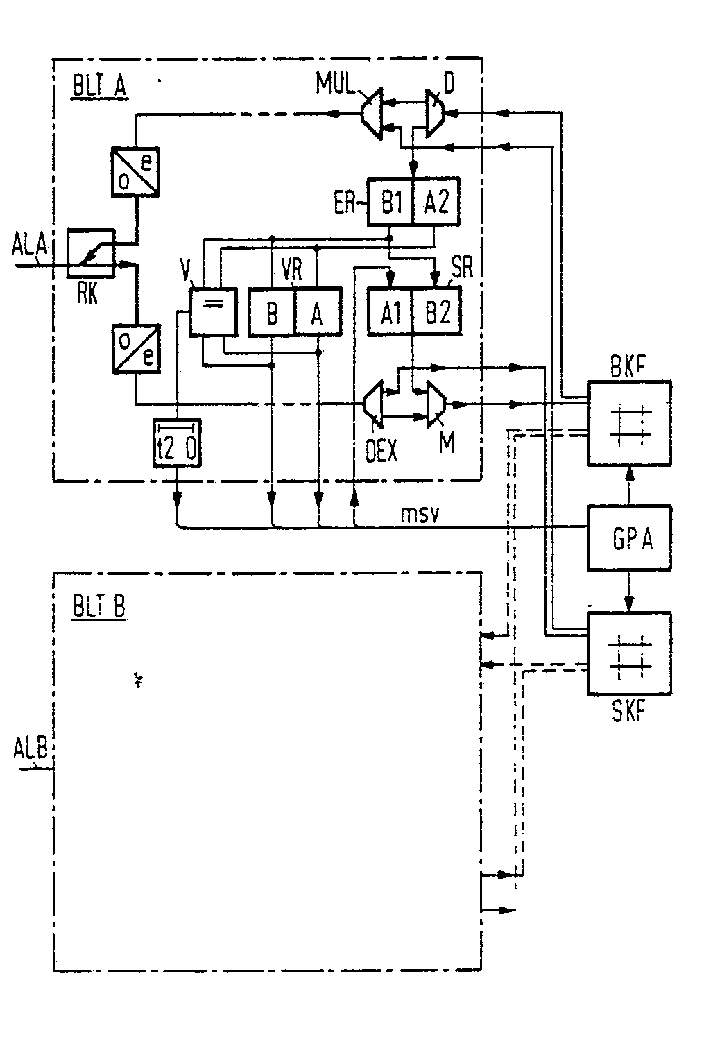
Description
In Fernmeldevermittlungsanlagen besteht neben deren Hauptaufgabe, Leitungsanschlüsse für einen exklusiven Nachrichtenaustausch zeitweilig miteinander zu verbinden, zugleich die Nebenaufgabe, fehlerhafte Verbindungen, insbesondere zwischen zwei bereits miteinander verbundenen Leitungsanschlüssen und einem dritten Leitungsanschluß (sog. Doppelverbindungen), zu vermeiden. Insbesondere in Breitband-Koppeleinrichtungen für Bildkommunikation kennt man außer steuerungsfehlerbedingten Fehlverbindungen auch Fehlverbindungen, die durch Nebensprecheffekte hervorgerufen werden. Nachdem solche Fehlverbindungen sporadisch auftreten können, müssen sie, um nachteilige Störungen vermeiden zu können, sehr schnell erkannt werden.In telecommunications switching systems, in addition to their main task of temporarily connecting line connections for an exclusive exchange of messages, there is also the secondary task of avoiding faulty connections, in particular between two line connections already connected to one another and a third line connection (so-called double connections). In particular in broadband coupling devices for image communication, in addition to faulty connections caused by control errors, faulty connections are also known which are caused by crosstalk effects. Since such faulty connections can occur sporadically, they have to be recognized very quickly in order to be able to avoid adverse interference.
Um Fehlverbindungen in Vermittlungsanlagen festzustellen, unterzieht man deren Koppeleinrichtungen sogenannten Durchschalteprüfungen. Das Konzept einer solchen Durchschalteprüfung muß dabei die Größe der Vermittlungsanlage, vermittlungstechnische Abläufe und ggf. eine Aufgabenteilung zwischen verschiedenen Vermittlungsprozessoren berücksichtigen.In order to determine faulty connections in switching systems, their coupling devices are subjected to so-called interconnection tests. The concept of such an interconnection test must take into account the size of the switching system, switching processes and, if necessary, a division of tasks between different switching processors.
So hat man zur Durchschalteprüfung einer Breitband-Koppeleinrichtung, über die Bildfernsprechsignale durchgeschaltet werden, vorgesehen, daß jeweils nach einer Verbindungsdurchschaltung bei dem jeweils einen an der betreffenden Verbindung beteiligten Leitungsanschluß der Koppeleinrichtung ein Pilotsignal eingespeist wird und dann geprüft wird, ob dieses Pilotsignal nur zu dem jeweils anderen an der betreffenden Verbindung beteiligten Leitungsanschluß der Koppeleinrichtung. (und zu keinem weiteren Anschluß) gelangt. Auf diese Art und Weise ist es an sich möglich, jede neu geschaltete Verbindung auf Durchschaltung und Doppelverbindung zu überprüfen; das Verfahren führt indessen wegen der jeweils erforderlichen Abfrage aller Leitungsanschlüsse schnell zu relativ großen Rechnerbelastungen und Verarbeitungszeiten, so daß es nur für sehr kleine Vermittlungsanlagen praktikabel ist.So it has been provided for the switching test of a broadband coupling device via which video telephone signals are switched through that a pilot signal is fed in each time after a connection has been switched through at each line connection of the coupling device involved in the connection in question, and then it is checked whether this pilot signal is only for the each other line connection of the coupling device involved in the relevant connection. (and no other connection). In this way it is possible in itself to check each newly switched connection for connection and double connection; the However, the method quickly leads to relatively large computer loads and processing times because of the respectively required query of all line connections, so that it is only practical for very small switching systems.
Für eine Vermittlungsanlage mit jeweils eine Vielzahl von (Teilnehmer-)Anschlüssen aufnehmenden, jeweils einen Gruppenkoppler und einen Gruppenprozessor aufweisenden (dezentralen) Anschlußgruppen, mit einem demgegenüber zentralen Koppelnetz und mit einem zentralen Koordinationsprozessor ist es (aus EP-A-01 63 288) bekannt, zur Durchschalteprüfung einer Raummultiplex-Koppeleinrichtung durch verbindungsindividuelles eingangsseitiges Einspeisen und ausgangsseitiges Auswerten einer Prüfinformation in der Weise zu verfahren, daß die Prüfinformation jeweils eine den für die betreffende Verbindung benutzten Eingang der Koppeleinrichtung kennzeichnende Absenderadresse sowie eine den zu benutzenden Ausgang der Koppeleinrichtung kennzeichnende Zieladresse umfaßt und empfangsseitig mit den durch diese Adressen gebildeten Verbindungsdaten verglichen wird,
wobei in einem Fernmeldesystem, bei dem auf den durch die Raummultiplex-Koppeleinrichtung zu verbindenden Leitungen in periodisch sich wiederholenden Zeitspannen außer der durchzuschaltenden Nutzinformation auch der Signalisierung, Steuerung und Synchronisierung dienende Betriebsinformationen übertragen werden,
entweder die Prüfinformationen nur während des Verbindungsaufbaues in den für die Nutzinformationen vorgesehenen Zeitspannen übertragen werden und empfangsseitig einmalig ein Vergleich mit den gespeicherten Einstellinformationen vor-genommen wird
oder aber die Prüfinformation während der gesamten Dauer einer Verbindung anstelle einer der Betriebsinformationen, die eingangs der Raummultiplex-Koppeleinrichtung ausgeblendet und ggfs. ausgangs der Raummultiplex-Koppeleinrichtung wieder zugeführt werden, in den für diese Betriebsinformationen vorge sehenen Zeitspannen über die Raummultiplex-Koppeleinrichtung übertragen werden und empfangsseitig periodisch ein Vergleich mit den gespeicherten Einstellinformationen vorgenommen wird; der dabei jeweils mit einer der betreffenden Ausgangsleitung individuell zugeordneten Einrichtung vorgenommene empfangsseitige Vergleich bedingt eine entsprechende empfangsseitige Verfügbarkeit der Verbindungsadressen.It is known (from EP-A-01 63 288) for a switching system with in each case a large number of (subscriber) connections, each having a group coupler and a group processor (decentralized) connection groups, with a central switching network and a central coordination processor to proceed for the through-connection test of a space-division multiplex switching device by connection-specific input-side feeding and output-side evaluation of test information in such a way that the test information in each case comprises a sender address which identifies the input of the switching device used for the connection in question and a destination address which identifies the output of the switching device to be used is compared on the receiving side with the connection data formed by these addresses,
in a telecommunications system in which operating information serving for signaling, control and synchronization is also transmitted on the lines to be connected by the space multiplex coupling device in periodically repeating periods in addition to the user information to be switched through,
either the test information is only transmitted during the establishment of the connection in the time periods provided for the useful information and a comparison is made once on the receiving side with the stored setting information
or the test information during the entire duration of a connection instead of one of the operating information, which is hidden at the beginning of the room multiplex coupling device and, if necessary, is fed out again from the room multiplex coupling device, in the operating information provided for this seen periods of time are transmitted via the space multiplex switching device and a periodic comparison with the stored setting information is carried out at the receiving end; the comparison on the receiving side, which is carried out individually with a device assigned to the respective output line, requires a corresponding availability of the connection addresses on the receiving side.
In solchem Zusammenhang ist auch schon vorgeschlagen worden (EP-86 103 038.5), zur Durchschalteprüfung einer Breitband-Koppeleinrichtung unter verbindungsindividuellem eingangsseitigen Einspeisen und ausgangsseitigem Auswerten eines eine den Koppeleinrichtungs-Eingang bezeichnende Adresse enthaltenden Prüfsignals in der Weise zu verfahren, daß in einem diensteintegrierenden Telekommunikationssystem mit getrennten Koppeleinrichtungen für Schmalband- und für Breitbanddienste in jeder an einer Breitbandverbindung beteiligten Anschlußleitung Durchschalteprüfsignale, die jeweils die Adresse eben dieser Anschlußschaltung sowie die in von der Gegenseite her empfangenen entsprechenden Durchschalteprüfsignalen etwa enthaltene Adressen der Gegen-Anschlußschaltung enthalten, in die Schmalbandsignallücken des Breitbandsignals eingefügt werden und von jeder Anschlußschaltung die Breitbandsignalübertragung über die zugehörige Anschlußleitung für zumindest eine Übertragungsrichtung nur bei Empfang eines die eigene Adresse enthaltenden Durchschalteprüfsignals freigegeben wird.
Diese Durchschalteprüfung ermöglicht es, bereits individuell von einem jeweils betroffenen Leitungsanschluß her ohne Mitwirkung übergeordneter Einrichtungen fehlerhafterweise nur in einer Richtung zustande kommende Verbindungen und (insbes. nebensprechbedingte) Doppelverbindungen rechtzeitig erkennen zu können, so daß sie gar nicht erst wirksam werden.
Dabei können die über die Breitband-Koppeleinrichtung durchvermittelten Digitalsignale einzeln auch an einen ebenfalls an die Breitband-Koppeleinrichtung angeschlossenen Prüf anschluß angeschaltet werden. Ein solcher Prüfanschluß, der sich zyklisch oder auch von Fall zu Fall gezielt an die einzelnen Leitungsanschlüsse anschalten kann, kann dem Digitalsignal die darin enthaltenen Durchschalteprüfsignale entnehmen und an den zugehörigen Vermittlungsprozessor weiterleiten, der damit die Richtigkeit der bestehenden Verbindung prüfen kann. Mit den Durchschalteprüfsignalen können auch zusätzliche Meldebits zum Prüfanschluß übertragen werden, die der Prüfanschluß dann auswerten und zum Vermittlungsprozessor weiterleiten kann.
Alternativ dazu ist es aber auch möglich, daß von den Anschlußschaltungen selbst über gesonderte Meldesignalverbindungen Meldebits zu dem übergeordneten Vermittlungsprozessor übertragen werden, womit dieser wiederum entsprechende Zusatzinformationen erhalten kann.In such a context, it has also already been proposed (EP-86 103 038.5) to proceed for the through-connection test of a broadband coupling device with connection-specific input-side feeding and output-side evaluation of a test signal containing an address designating the coupling device input in such a way that in an integrated service telecommunications system with separate coupling devices for narrowband and for broadband services in each connection line involved in a broadband connection, through-test signals, each containing the address of this connection circuit as well as the addresses of the counter-connection circuit contained in the corresponding through-test signals received from the opposite side, inserted into the narrowband signal gaps of the broadband signal and the broadband signal transmission from each connection circuit via the associated connection line for at least one transmission direction only upon receipt nes switching test signal containing its own address is released.
This interconnection test makes it possible to identify connections in one direction and (in particular. Crosstalk-related) double connections that have already been made in a faulty manner from an affected line connection without the involvement of higher-level facilities, so that they do not become effective at all.
The digital signals transmitted through the broadband coupling device can also be sent individually to a test that is also connected to the broadband coupling device connection can be switched on. Such a test connection, which can be connected cyclically or on a case-by-case basis to the individual line connections, can take the circuit test signals contained therein from the digital signal and pass them on to the associated switching processor, which can thus check the accuracy of the existing connection. With the interconnection test signals, additional signaling bits can also be transmitted to the test connection, which the test connection can then evaluate and forward to the switching processor.
As an alternative to this, it is also possible for the connection circuits themselves to transmit message bits to the superordinate switching processor via separate message signal connections, which in turn can receive corresponding additional information.
Diese bekannte Verfahrensweise ermöglicht in ihrer zuletzt angesprochenen Alternative eine dezentrale, rein anschlußbezogene Durchschalteprüfung einer Breitband-Koppeleinrichtung bereits unter Verzicht auf besondere Prüfanschlüsse und damit unter Vermeidung von mit der Verwendung von Prüfanschlüssen verbundenen Umständen wie etwa des Erfordernisses, in einem Steuerungsablauf auf die Zuteilung eines der in begrenzter Zahl verfügbaren Prüfanschlüsse warten zu müssen oder der Notwendigkeit zusätzlicher Abläufe für Routineprüfungen semipermanenter Verbindungen, - womit sogleich dem jeweiligen Vermittlungsprozessor entsprechende Koordinierungsleistungen erspart werden.
Eine solche gewissermaßen "symmetrische" Auswertung jeweils nur der in dem von der Gegenseite her empfangenen Durchschalteprüfsignal etwa enthaltenen eigenen Adresse durch jeweils beide an einer Verbindung beteiligte Anschlußschaltungen überläßt es indessen dem übergeordneten Vermittlungsprozessor, von verschiedenen Anschlußschaltungen her eintreffende Meldebits miteinander in Beziehung zu setzen und damit der jeweiligen Verbindung zuzuordnen.In its last-mentioned alternative, this known procedure enables a decentralized, purely connection-related through-connection test of a broadband coupling device, even without special test connections and thus avoiding the circumstances associated with the use of test connections, such as the requirement in a control process for the assignment of one of the having to wait in a limited number of available test connections or the need for additional processes for routine tests of semi-permanent connections, - so that the respective switching processor is spared corresponding coordination services.
Such a so-called "symmetrical" evaluation of only the own address contained in the through-test signal received from the opposite end by each of the two connection circuits involved in a connection, however, leaves it to the higher-level switching processor to relate the incoming message bits coming from different connection circuits to one another, and thus assign to the respective connection.
Die Erfindung stellt sich nun die Aufgabe einer weiteren Dezentralisierung der Durchschalteprüfung einer Breitband-Koppeleinrichtung.
Die Erfindung betrifft ein Verfahren zur Durchschalteprüfung einer Breitband-Koppeleinrichtung unter verbindungsindividuellem eingangsseitigen Einspeisen und ausgangsseitigen Auswerten eines eine den Koppeleinrichtungs-Eingang bezeichnende Adresse enthaltenden Prüfsignals,
demzufolge in einem diensteintegrierenden Telekommunikationssystem mit getrennten Koppeleinrichtungen für Schmalband- und für Breitbanddienste in jeder an einer Breitbandverbindung beteiligten Anschlußschaltung Durchschalteprüfsignale, die jeweils die Adresse eben dieser Anschlußschaltung sowie die in von der Gegenseite her empfangenen entsprechenden Durchschalteprüfsignalen etwa enthaltene Adresse der Gegen-Anschlußschaltung enthalten, in schmalbandige Signallücken des Breitbandsignals eingefügt werden;
dieses Verfahren ist erfindungsgemäß dadurch gekennzeichnet, daß in einer der beiden an einer Verbindung beteiligten Anschlußschaltungen die von der Gegen-Anschlußschaltung her empfangenen Durchschalteprüfsignale auf das Auftreten sowohl der eigenen Adresse als auch der Adresse der Gegen-Anschlußschaltung überprüft werden und zumindest bei Nichtauftreten wenigstens einer der beiden Adressen ein das Prüfergebnis meldendes Signal von der Anschlußschaltung zu dem ihr zugehörigen Vermittlungsprozessor übertragen wird.The object of the invention is now to further decentralize the interconnection test of a broadband switching device.
The invention relates to a method for the through-connection test of a broadband switching device with connection-specific input-side feeding and output-side evaluation of a test signal containing an address identifying the switching device input.
consequently in an integrated service telecommunication system with separate coupling devices for narrowband and for broadband services in each connection circuit involved in a broadband connection, through-test signals which each contain the address of this connection circuit as well as the address of the counter-connection circuit contained in the corresponding connection test signals received from the opposite side, in narrowband signal gaps of the wideband signal are inserted;
According to the invention, this method is characterized in that in one of the two connection circuits involved in a connection, the interconnection test signals received from the counter-connection circuit are checked for the occurrence of both the own address and the address of the counter-connection circuit, and at least one of the at least if no one occurs Both addresses a signal reporting the test result is transmitted from the connection circuit to the associated switching processor.
Eine solche Durchschalteprüfung mit einer gewissermaßen unsymmetrischen Auswertung der Durchschalteprüfsignale ermöglicht die Zusammenführung der in den Durchschalteprüfsignalen enthaltenen Adressen der beiden an einer Verbindung beteiligten Anschlußschaltungen bereits in einer solchen Anschlußschaltung selbst und vermeidet damit eine entsprechende Belastung des zugehörigen Vermittlungsprozessors; der Vermittlungsprozessor kann vielmehr bereits die Adressen beider an einer Verwendung beteiligten Anschluß schaltungen zusammen von der betreffenden einen Anschlußschaltung übernehmen.Such an interconnection test with a somewhat asymmetrical evaluation of the interconnection test signals enables the addresses of the two connection circuits involved in a connection to be combined in such a connection circuit itself and thus avoids a corresponding load on the associated switching processor; rather, the switching processor can already have the addresses of both ports involved in use circuits together from the relevant take over a connection circuit.
Dabei können in der betreffenden Anschlußschaltung die Durchschalteprüfsignale ständig auf (nachhaltige) Änderungen überprüft werden, und es wird dann in weiterer Ausgestaltung der Erfindung ein Meldesignal nur nach einer Änderung des Durchschalteprüfsignals übertragen, was zu einer entsprechend geringen Beanspruchung des Vermittlungsprozessors durch solche Meldesignale führt.The circuit test signals can be continuously checked for (sustainable) changes in the connection circuit in question, and in a further embodiment of the invention a signal is then only transmitted after a change in the circuit test signal, which leads to a correspondingly low load on the switching processor by such signal signals.
Es ist aber auch möglich, daß in der betreffenden Anschlußschaltung die Durchschalteprüfsignale ständig mit einem entsprechend dem jeweiligen Verbindungszustand vom zugehörigen Vermittlungsprozessor vorgegebenen Sollsignal verglichen werden, und es wird dann in weiterer Ausgestaltung der Erfindung ein Meldesignal nur bei einer Abweichung des Durchschalteprüfsignals vom jeweiligen Sollsignal übertragen, was ebenfalls zu einer entsprechend geringen Beanspruchung des Vermittlungsprozessors führt.However, it is also possible that the circuit test signals in the connection circuit in question are constantly compared with a target signal specified by the associated switching processor in accordance with the respective connection state, and in a further embodiment of the invention a message signal is then only transmitted if the circuit test signal differs from the respective target signal, which also leads to a correspondingly low load on the switching processor.
Weitere Besonderheiten der Erfindung werden aus deren nachfolgender näherer Erläuterung an Hand der Zeichnung ersichtlich.Further special features of the invention will become apparent from the following detailed explanation with the aid of the drawing.
In der Zeichnung ist schematisch in einem zum Verständnis der Erfindung erforderlichen Umfang ein Ausführungsbeispiel eines diensteintegrierenden Telekommunikationssystems mit einer von einem Vermittlungsprozessor GP A gesteuerten Schmalbandkoppeleinrichtung SKF und einer gesonderten, vorzugsweise von demselben Vermittlungsprozessor GP A gesteuerten Breitbandkoppeleinrichtung BKF dargestellt, an die zu Teilnehmerstationen oder auch zu anderen Vermittlungseinrichtungen führende Lichtwellenleiter-Anschlußleitungen AL A,.. ..,AL B jeweils über eine Anschlußschaltung BLT A,...,BLT B angeschlossen sind.In the drawing, an embodiment of an integrated service telecommunication system with a narrowband switching device SKF controlled by a switching processor GP A and a separate broadband switching device BKF, preferably controlled by the same switching processor GP A, to the to subscriber stations or to is shown schematically to an extent necessary for understanding the invention other switching devices leading fiber optic connection lines AL A, .. .., AL B are each connected via a connection circuit BLT A, ..., BLT B.
Es sei dazu bemerkt, daß die Anschlußschaltungen in jeweils eine Vielzahl von (Teilnehmer-)Anschlüssen aufnehmenden, jeweils einen Gruppenkoppler und einen Gruppenprozessor aufweisenden (dezentralen) Anschlußgruppen zusammengefasst sein können uns daß das Telekommunikationssystem ausserdem ein demgegenüber zentrales Koppelnetz und einen zentralen Koordinationsprozessor aufweisen kann, wobei dann die in der Zeichnung dargestellte Koppeleinrichtung jeweils für den jeweiligen Gruppenkoppler und/oder das zentrale Koppelnetz steht und der in der Zeichnung dargestellte Vermittlungsprozessor GP A für den Gruppenprozessor und/oder den zentralen Koordinationsprozessor.It should be noted that the connection circuits can each be grouped into a plurality of (subscriber) connections, each with a group coupler and a group processor (decentralized) connection groups and that the telecommunication system can also have a central switching network and a central coordination processor. the coupling device shown in the drawing then stands for the respective group coupler and / or the central switching network and the switching processor GP A shown in the drawing for the group processor and / or the central coordination processor.
Aus der die Anschlußschaltung BLT A näher in schaltungstechnischen Einzelheiten zeigenden Zeichnung wird dabei ersichtlich, daß die - dann einfaserige - Lichtwellenleiter-Anschlußleitung AL in der Anschlußschaltung BLT über einen Lichtwellenleiter-Richtungskoppler RK mit dem Ausgang eines elektro/optischen Wandlers e/o und mit dem Eingang eines opto/elektrischen Wandlers o/e verbunden sein kann. Mit dem Eingang des elektro/optischen Wandlers e/o ist der Ausgang eines Multiplexers MUL verbunden, der über die Schmalbandkoppeleinrichtung SKF durchvermittelte Schmalband-Digitalsignale (z.B. 64-kbit/-Fernsprechsignale) und über die Breitbandkoppeleinrichtung BKF durchvermittelte Breitbandsignale (Bildsignale) sowie (z.B. 8-kbit/s-)Steuersignale und Synchronisiersignale zu einem über die Lichtwellenleiter-Anschlußleitung AL zu übertragenden Multiplexsignal, beispielsweise einem etwa einen sog. H4-Kanal ausfüllenden 140-Mbit/s-Zeitmultiplexsignal oder einem etwa einen sog. H1-Kanal ausfüllenden 2-Mbit/s-Zeitmultiplexsignal, zusammenfaßt. Ein in der umgekehrten Übertragungsrichtung über die Lichtwellenleiter-Anschlußleitung AL übertragenes Multiplexsignal, insbesondere Zeitmultiplexsignal, wird in einem dem opto/elektrischen Wandler o/e nachgeschalteten Demultiplexer DEX in die entsprechenden Einzelsignale, beispielsweise in (z.B. 8-kbit/s-)Steuersignale, Synchronisiersignale, über die Schmalbandkoppeleinrichtung SKF durchzuvermittelnde (z.B. 64-kbit/s-Fernsprech-)Schmalband-Digitalsignale und ein über die Breitbandkoppeleinrichtung BKF durchzuschaltendes Breitbandsignal (Bildsignal), aufgefächert.From the drawing showing the connection circuit BLT A in more detail in terms of circuitry, it can be seen that the - then single-fiber - optical fiber connecting line AL in the connection circuit BLT via an optical fiber directional coupler RK with the output of an electro / optical converter e / o and with the Input of an opto / electrical converter o / e can be connected. The output of a multiplexer MUL is connected to the input of the electro / optical converter e / o, which transmits narrowband digital signals (e.g. 64 kbit / telephone signals) via the narrowband coupling device SKF and broadband signals (image signals) transmitted via the broadband coupling device BKF and (e.g. 8 kbit / s) control signals and synchronization signals for a multiplex signal to be transmitted via the optical fiber connecting line AL, for example a 140 Mbit / s time-division multiplex signal which fills an H4 channel or an H1 channel 2 -Mbit / s time division multiplex signal, summarized. A multiplex signal, in particular time-division multiplex signal, which is transmitted in the reverse transmission direction via the optical waveguide connecting line AL, is converted into the corresponding individual signals, for example in, in a demultiplexer DEX connected downstream of the opto / electrical converter (eg 8 kbit / s) control signals, synchronization signals, narrow band digital signals to be transmitted via the narrow band switching device SKF (eg 64 kbit / s telephone) and a broadband signal (picture signal) to be switched through the broad band switching device BKF.
In nach einer solchen Auffächerung bestehende schmalbandige Signallücken des Breitbandsignals werden nun in einer an einer Breitbandverbindung beteiltigen Anschlußschaltung BLT während der ganzen Verbindungsdauer Durchschalteprüfsignale eingefügt, die jeweils die Adresse eben dieser Anschlußschaltung BLT sowie ggf. die in von der Gegenseite her über die Breitbandkoppeleinrichtung BKF empfangenen entsprechenden Durchschalteprüfsignalen enthaltene Adresse einer Gegen-Anschlußschaltung enthalten. Wie aus der Zeichnung ersichtlich wird, kann dazu in jeder Anschlußschaltung BLT ein Senderegister SR vorgesehen sein, in dessen ersten Registerteil A1, vom Vermittlungsprozessor GP A her jeweils eingegeben (oder auch ständig), die Adresse eben dieser Anschlußschaltung stehen möge und in dessen zweiten Registerteil B2 ggf. die empfangene Adresse einer Gegen-Anschlußschaltung eingegeben wird; ausgangsseitig führt das Senderegister SR zu einem entsprechenden Eingang eines Multiplexers M, der zwischen den Demultiplexer DEX und die Breitbandkoppeleinrichtung BKF eingefügt ist, so daß er das vom Senderegister SR jeweils abgegebene Durchschalteprüfsignal in eine Signallücke des Breitbandsignals einfügt.
Es sei hier bemerkt, daß die Erfindung auch dann Anwendung finden kann, wenn auf der Anschlußleitung AL an sich gar kein Schmalbandsignal übertragen wird; es genügt vielmehr, davon auszugehen, daß im Breitbandsignal eine schmalbandige (beispielsweise 4-kbit/s-)Signallücke (beispielsweise in Form einer Bitposition in jedem zweiten Rahmen) zur Aufnahme des Durchschalteprüfsignals verfügbar ist.In such narrow band signal gaps of the broadband signal existing in a broadband connection involved in a connection circuit BLT through-connection test signals are inserted throughout the entire connection duration, each the address of this connection circuit BLT and possibly the corresponding received from the opposite side via the broadband switching device BKF Switch-through test signals contain the address of a counter-connection circuit. As can be seen from the drawing, a transmit register SR can be provided for this in each connection circuit BLT, in the first register part A1 of which the switching processor GP A entered (or also constantly) the address of this connection circuit may be located and in the second register part thereof B2 if necessary, the received address of a counter-connection circuit is entered; on the output side, the transmission register SR leads to a corresponding input of a multiplexer M, which is inserted between the demultiplexer DEX and the broadband coupling device BKF, so that it inserts the interconnection test signal emitted by the transmission register SR into a signal gap of the broadband signal.
It should be noted here that the invention can also be used when no narrowband signal is actually transmitted on the connecting line AL; it is rather sufficient to assume that a narrow-band (for example 4 kbit / s) signal gap (for example in the form of a bit position in every other frame) is available in the broadband signal for receiving the circuit test signal.
Im umgekehrt gerichteten Signalweg ist zwischen die Breitbandkoppeleinrichtung BKF und den Multiplexer MUL ein Demultiplexer D eingefügt, der solche von einer mit der gerade betrachteten Anschlußleitung BLT A über die Breitbandkoppeleinrichtung BKF gerade verbundenen anderen Anschlußschaltung in das Breitbandsignal eingefügte Durchschalteprüfsignale ausblendet und einem Empfangsregister ER zuführt. Dessen erster Registerteil B1, der ggf. die in einem solchen Durchschalteprüfsignal enthaltene Adresse einer mit der gerade betrachteten Anschlußschaltung BLT A über die Breitbandkoppeleinrichtung BKF gerade verbundenen Gegen-Anschlußschaltung, beispielsweise der in gleicher Weise aufgebauten Anschlußschaltung BLT B, aufnimmt, ist mit dem Senderegisterteil B2 verbunden, so daß die in in der Anschlußschaltung BLT A empfangenen Durchschalteprüfsignalen enthaltene Adresse der Gegen-Anschlußschaltung (BLT B) in diesen Senderegisterteil B2 gelangt und dann, wie schon erwähnt, in den nachfolgend von der gerade betrachteten Anschlußschaltung BLT A abzugebenden Durchschalteprüfsignalen an die Adresse eben dieser Anschlußschaltung BLT A angefügt und damit zur Gegen-Anschlußschaltung (BLT B) zurückübertragen wird.A demultiplexer D is inserted in the reverse signal path between the broadband switching device BKF and the multiplexer MUL. Its first register part B1, which possibly contains the address contained in such a circuit test signal of a counter-connection circuit currently connected to the connection circuit BLT A under consideration via the broadband switching device BKF, for example the connection circuit BLT B constructed in the same way, is with the transmission register part B2 connected so that the address of the counter-connection circuit (BLT B) contained in the connection circuit BLT A received in this transmission register part B2 and then, as already mentioned, in the connection test signals to be subsequently emitted by the connection circuit BLT A under consideration to the address just added this connection circuit BLT A and is thus transmitted back to the counter-connection circuit (BLT B).
In entsprechender Weise wird, ohne daß dies in der Zeichnung noch näher verdeutlicht ist, in der im Beispiel gerade mit der Anschlußschaltung BLT A über die Breitbandkoppeleinrichtung BKF verbundenen Anschlußschaltung BLT B die in den dort von der Anschlußschaltung BLT A her empfangenen Durchschalteprüfsignalen enthaltene Adresse der Anschlußschaltung BLT A in den von der Anschlußschaltung BLT B ausgesendeten Durchschalteprüfsignalen gewissermaßen reflektiert. Die reflektierte Adresse gelangt dann bei Empfang dieser Durchschaltesignale in der Anschlußschaltung BLT A in deren Empfangsregisterteil A2.Correspondingly, without this being clarified in the drawing, in the connection circuit BLT B connected to the connection circuit BLT A via the broadband coupling device BKF in the example, the address of the connection circuit contained in the circuit test signals received there by the connection circuit BLT A BLT A is reflected to a certain extent in the interconnection test signals emitted by the connection circuit BLT B. When these switching signals are received, the reflected address then arrives in the connection circuit BLT A in its reception register part A2.
In einer der beiden an einer Verbindung beteiligten Anschlußschaltungen BLT, beispielsweise in der Anschlußschaltung des rufenden Teilnehmers, werden nun die von der Gegen-Anschlußschaltung her empfangenen Durchschalteprüfsignale auf das Auftreten sowohl der eigenen Adresse als auch der Adresse der Gegen-Anschlußschaltung überprüft. In der Zeichnung ist dazu für die Anschlußschaltung BLT A angedeutet, daß ein Vergleicher V jeweils die beiden mit dem gerade empfangenen Durchschalteprüfsignal in das Empfangsregister ER gelangten Adressen mit zwei in einem Vergleichsregister VR in entsprechenden Registerteilen A und B stehenden entsprechenden Adressen vergleicht. Dabei können, wie dies auch in der Zeichnung angedeutet ist, im Vergleichsregister VR die im jeweils zuletzt empfangenen Durchschalteprüfsignal enthaltenen beiden Adressen stehen, so daß dann der Vergleicher V Änderungen des Durchschalteprüfsignals festzustellen vermag; ohne daß dies in der Zeichnung im einzelnen dargestellt ist, ist es aber auch möglich, vom zugehörigen Vermittlungsprozessor GP A her jeweils bei einem Verbindungsaufbau die Adressen der beiden an der Verbindung beteiligten Anschlußschaltungen als Sollsignal in das Vergleichsregister VR einzugeben, so daß der Vergleicher V dann Abweichungen des Durchschalteprüfsignals vom jeweiligen Sollsignal festzustellen vermag.
Zumindest bei Nichtauftreten wenigstens einer der beiden Adressen im jeweils gerade empfangenen Durchschalteprüfsignal wird dann ein das Prüfergebnis meldendes Signal von der Anschlußschaltung BLT A über eine entsprechende Meldesignalverbindung msv zum zugehörigen Vermittlungsprozessor GP A übertragen, der daraufhin die beiden Anschlußschaltungsadressen aus der Anschlußschaltung BLT A über die Meldesignalverbindung msv entnehmen kann, um daraus entsprechende Folgerungen zu ziehen. Dabei wird, wie dies auch in der Zeichnung angedeutet ist, der Vergleicher V zweckmäßigerweise mit einer Abfallverzögerung versehen, so daß die Meldesignalübertragung bei einer Änderung des Durchschalte prüfsignals für eine Verzögerungszeitspanne t2 unterbleibt und somit Einzelfehler bei der Übertragung der Durchschalteprüfsignale nicht zu einer Meldesignalgabe führen. Unter der Annahme, daß eine Änderung des Durchschalteprüfsignals erst dann als erkannt gewertet wird, wenn das geänderte Durchschalteprüfsignal viermal empfangen wurde, kann man bei einem ein Flag und die beiden Anschlußschaltungsadressen enthaltenden, beispielswseise 40 bis 46 bit langen Durchschalteprüfsignal mit einer Überprüfungszeit von
4 × 46 bit / 4 kbit/s = 46 ms
rechnen.In one of the two connection circuits BLT involved in a connection, for example in the connection circuit of the calling subscriber, the interconnection test signals received from the counter-connection circuit are now checked for the occurrence of both the own address and the address of the counter-connection circuit. In the drawing, it is indicated for the connection circuit BLT A that a comparator V compares the two addresses which have just entered the reception register ER with the circuit test signal just received with two corresponding addresses in a comparison register VR in corresponding register parts A and B. Here, as is also indicated in the drawing, the two addresses contained in the most recently received circuit test signal can be found in the comparison register VR, so that the comparator V can then determine changes in the circuit test signal; Without this being shown in detail in the drawing, it is also possible to enter the addresses of the two connection circuits involved in the connection as a desired signal in the comparison register VR from the associated switching processor GP A each time a connection is established, so that the comparator V then Deviations of the switching test signal from the respective target signal can determine.
At least if at least one of the two addresses does not appear in the circuit test signal just received, a signal reporting the test result is then transmitted from the connection circuit BLT A via a corresponding message signal connection msv to the associated switching processor GP A, which then transmits the two connection circuit addresses from the connection circuit BLT A via the message signal connection msv can take to draw appropriate conclusions. In this case, as is also indicated in the drawing, the comparator V is expediently provided with a drop-out delay, so that the signal transmission when there is a change in the switching test signal for a delay period t2 is omitted and thus individual errors in the transmission of the switching test signals do not lead to a signaling signal. Assuming that a change in the interconnection test signal is only considered to be recognized if the changed interconnection test signal has been received four times, one can, for example, a 40 to 46 bit long interconnection test signal containing a flag and the two connection circuit addresses with a check time of
4 × 46 bit / 4 kbit / s = 46 ms
count.
Mit der beschriebenen Durchschalteprüfung wird der Vermittlungsprozessor von Steuerungsleistungen für die Prüfung und Überwachung des Koppelnetzes weitgehend freigestellt:
Zur Durchschalteprüfung meldet sich die auf der rufenden Verbindungsseite liegende Anschlußschaltung BLT von sich aus mit den Adressen der an der Verbindung beteiligten Anschlußschaltungen, sobald die Verbindung im Koppelnetz eingestellt ist; fehlerhafte Verbindungen äußern sich in falschen Adressen.
Nach der Durchschalteprüfung ergibt sich von selbst eine - besonders für semipermanente Verbindungen bedeutsame - ständige Überwachung der bestehenden Verbindung, wobei die auf der rufenden Verbindungsseite liegende Anschlußschaltung BLT spontan bei Auftreten eines Verbindungsfehlers reagiert.
Mit der Durchschalteprüfung bzw. Verbindungsüberwachung werden zugleich die die Durchschalteprüfung bzw. Verbindungsüberwachung durchführenden Schaltungen im Betrieb mitgetestet, wobei aber auch eine gezielte Prüfung durch Schalten von Pseudoverbindungen im Koppelnetz nicht ausgeschlossen ist.With the interconnection test described, the switching processor is largely exempt from control services for testing and monitoring the switching network:
For the connection test, the connection circuit BLT on the calling connection side reports itself with the addresses of the connection circuits involved in the connection as soon as the connection is set in the switching network; faulty connections are expressed in wrong addresses.
After the interconnection test, there is a constant monitoring of the existing connection, which is particularly important for semi-permanent connections, the connection circuit BLT on the calling connection side reacting spontaneously when a connection error occurs.
With the interconnection test or connection monitoring, the circuits performing the interconnection test or connection monitoring are also tested in operation, but a targeted test by switching pseudo connections in the switching network is not excluded.
- A1 erster Registerteil (im SR)A1 first part of the register (in the SR)
- A2 zweiter Registerteil (Empfangsregisterteil)A2 second register part (receiving register part)
- AL A, AL B Lichtwellenleiter-AnschließleitungenAL A, AL B fiber optic connection cables
- A, B Registerteile (im VR)A, B register parts (in VR)
- B1 erster Registerteil (im ER)B1 first part of the register (in the ER)
- B2 zweiter Registerteil (Senderegisterteil)B2 second register part (transmission register part)
- BKF BreitbandkoppeleinrichtungBKF broadband switching facility
- BLT A, BLT B AnschlußschaltungenBLT A, BLT B connection circuits
- D DemultiplexerD demultiplexer
- DEX DemultiplexerDEX demultiplexer
- ER EmpfangsregisterER receive register
- e/o elektro/optischer Wandlere / o electro / optical converter
- GPA VermittlungsprozessorGPA mediation processor
- M MultiplexerM multiplexer
- MUL MultiplexerMUL multiplexer
- msv Meldesignalverbindungmsv signaling signal connection
- o/e Opto/elektrischer Wandlero / e opto / electrical converter
- RK Lichtwellenleiter-RichtungskopplerRK fiber optic directional coupler
- SKF SchmalbandkoppeleinrichtungSKF narrow band coupling device
- SR SenderegisterSR transmission register
- V VergleicherV comparator
- VR VergleichsregisterVR comparison register
Claims (3)
demzufolge in einem diensteintegrierenden Telekommunikationssystem mit getrennten Koppeleinrichtungen (SKF, BKF) für Schmalband- und für Breitbanddienste in jeder an einer Breitbandverbindung beteiligten Anschlußschaltung (BLT) Durchschalteprüfsignale, die jeweils die Adresse eben dieser Anschlußschaltung (BLT A) sowie die in von der Gegenseite her empfangenen entsprechenden Durchschalteprüfsignalen etwa enthaltene Adresse der Gegen-Anschlußschaltung (BLT B) enthalten, in schmalbandige Signallücken des Breitbandsignals eingefügt werden,
dadurch gekennzeichnet,
daß in einer der beiden an einer Verbindung beteiligten Anschlußschaltungen (BLT A) die von der Gegen-Anschlußschaltung (BLT B) her empfangenen Durchschalteprüfsignale auf das Auftreten sowohl der eigenen Adresse als auch der Adresse der Gegen-Anschlußschaltung (BLT B) überprüft werden und zumindest bei Nichtauftreten wenigstens einer der beiden Adressen ein das Prüfergebnis meldendes Signal von der Anschlußschaltung (BLT A) zu dem ihr zugehörigen Vermittlungsprozessor (GP A) übertragen wird.1. Method for the through-connection test of a broadband switching device with connection-specific input-side feeding and output-side evaluation of a test signal containing an address which designates the switching device input,
consequently in an integrated service telecommunication system with separate coupling devices (SKF, BKF) for narrowband and for broadband services in each connection circuit (BLT) involved in a broadband connection, interconnection test signals, each of which contains the address of this connection circuit (BLT A) as well as that received from the opposite side corresponding switching test signals contain any address of the counter-connection circuit (BLT B), are inserted into narrowband signal gaps of the broadband signal,
characterized,
that in one of the two connection circuits (BLT A) involved in a connection, the interconnection test signals received from the counter-connection circuit (BLT B) are checked for the occurrence of both the own address and the address of the counter-connection circuit (BLT B) and at least if at least one of the two addresses does not occur, a signal reporting the test result is transmitted from the connection circuit (BLT A) to the associated switching processor (GP A).
dadurch gekennzeichnet,
daß ein Meldesignal nur nach einer Änderung des Durchschalteprüfsignals übertragen wird.2. The method according to claim 1,
characterized,
that a message signal is only transmitted after a change in the switching test signal.
dadurch gekennzeichnet,
daß ein Meldesignal nur bei einer Abweichung des Durchschalteprüfsignals von einem Sollsignal übertragen wird.3. The method according to claim 1,
characterized,
that a message signal is only transmitted when the switching test signal deviates from a target signal.
Priority Applications (1)
| Application Number | Priority Date | Filing Date | Title |
|---|---|---|---|
| AT87107617T ATE101952T1 (en) | 1986-06-02 | 1987-05-25 | PROCEDURE FOR CONNECTION TESTING OF A BROADBAND COUPLING EQUIPMENT. |
Applications Claiming Priority (2)
| Application Number | Priority Date | Filing Date | Title |
|---|---|---|---|
| DE3618522 | 1986-06-02 | ||
| DE3618522 | 1986-06-02 |
Publications (3)
| Publication Number | Publication Date |
|---|---|
| EP0248325A2 true EP0248325A2 (en) | 1987-12-09 |
| EP0248325A3 EP0248325A3 (en) | 1989-12-20 |
| EP0248325B1 EP0248325B1 (en) | 1994-02-23 |
Family
ID=6302125
Family Applications (1)
| Application Number | Title | Priority Date | Filing Date |
|---|---|---|---|
| EP87107617A Expired - Lifetime EP0248325B1 (en) | 1986-06-02 | 1987-05-25 | Method for the through-connection testing of a broadband switching network |
Country Status (3)
| Country | Link |
|---|---|
| EP (1) | EP0248325B1 (en) |
| AT (1) | ATE101952T1 (en) |
| DE (1) | DE3789123D1 (en) |
Cited By (1)
| Publication number | Priority date | Publication date | Assignee | Title |
|---|---|---|---|---|
| DE3821871A1 (en) * | 1988-06-29 | 1990-01-18 | Philips Patentverwaltung | Broadband coupling device |
Family Cites Families (3)
| Publication number | Priority date | Publication date | Assignee | Title |
|---|---|---|---|---|
| US4439826A (en) * | 1981-07-20 | 1984-03-27 | International Telephone & Telegraph Corporation | Diagnostic system for a distributed control switching network |
| DE3566482D1 (en) * | 1984-05-29 | 1988-12-29 | Siemens Ag | Method for testing switched connexions of a multiplex space division switching network |
| JPS6148266A (en) * | 1984-08-15 | 1986-03-08 | Fujitsu Ltd | Time division multiplex line loop back test method |
-
1987
- 1987-05-25 EP EP87107617A patent/EP0248325B1/en not_active Expired - Lifetime
- 1987-05-25 AT AT87107617T patent/ATE101952T1/en not_active IP Right Cessation
- 1987-05-25 DE DE87107617T patent/DE3789123D1/en not_active Expired - Fee Related
Cited By (1)
| Publication number | Priority date | Publication date | Assignee | Title |
|---|---|---|---|---|
| DE3821871A1 (en) * | 1988-06-29 | 1990-01-18 | Philips Patentverwaltung | Broadband coupling device |
Also Published As
| Publication number | Publication date |
|---|---|
| EP0248325B1 (en) | 1994-02-23 |
| DE3789123D1 (en) | 1994-03-31 |
| EP0248325A3 (en) | 1989-12-20 |
| ATE101952T1 (en) | 1994-03-15 |
Similar Documents
| Publication | Publication Date | Title |
|---|---|---|
| DE3902243A1 (en) | METHOD FOR SWITCHING DIGITAL SIGNAL CONNECTIONS IN TRANSMISSION NETWORKS | |
| DE2714368C3 (en) | Circuit arrangement for switching through data words with different bit rate frequencies in multiple connections | |
| DE69634149T2 (en) | OPTICAL KNOT IN AN OPTICAL BUS NETWORK | |
| EP0428089B1 (en) | Subscriber node of a digital data transmission system | |
| EP0163288B1 (en) | Method for testing switched connexions of a multiplex space division switching network | |
| EP0173274B1 (en) | Method and circuit arrangement for realizing and maintaining a time division broadband connection | |
| EP0248325B1 (en) | Method for the through-connection testing of a broadband switching network | |
| EP0284106A2 (en) | Circuitry for inserting a service channel for an information transmission system | |
| EP0193967B1 (en) | Method for connection-testing of a broad-band switching network | |
| EP0198203B1 (en) | Method for connection-testing of a broad-band switching network | |
| EP0126413B1 (en) | Telecommunication system for stream traffic as well as for burst traffic | |
| DE2316478C3 (en) | Method for testing and maintaining the functionality of a time division multiplex switching network | |
| DE3789137T2 (en) | Method for expanding the transmission capacity in a network transmission system for optical subscribers. | |
| DE3821871C2 (en) | ||
| AT390857B (en) | CIRCUIT ARRANGEMENT FOR MEDIATING DATA SIGNALS DIFFERENT DATA SIGNAL RATES IN A DATA SWITCHING SYSTEM | |
| EP0023297B1 (en) | Digital telecommunication system | |
| DE69434309T2 (en) | Time Division Multiple Access Fiber Optic Digital Communication System | |
| DE3932700C2 (en) | Procedure for the interconnection test of a switching network | |
| DE2849348C2 (en) | ||
| DE3513181A1 (en) | Circuit arrangement for telecommunications switching systems, in particular telephone switching systems, with devices for functional capability testing of switched connections | |
| EP0984658B1 (en) | Telecommunication system with switching device and data concentrator for access to Internet | |
| DE19549149A1 (en) | Digital communication signal transmission control system | |
| DE3307347C2 (en) | ||
| DE3843182C2 (en) | ||
| DE4227736B4 (en) | Network with a branch and channel distribution device |
Legal Events
| Date | Code | Title | Description |
|---|---|---|---|
| PUAI | Public reference made under article 153(3) epc to a published international application that has entered the european phase |
Free format text: ORIGINAL CODE: 0009012 |
|
| AK | Designated contracting states |
Kind code of ref document: A2 Designated state(s): AT BE CH DE FR GB IT LI NL SE |
|
| PUAL | Search report despatched |
Free format text: ORIGINAL CODE: 0009013 |
|
| AK | Designated contracting states |
Kind code of ref document: A3 Designated state(s): AT BE CH DE FR GB IT LI NL SE |
|
| 17P | Request for examination filed |
Effective date: 19900528 |
|
| 17Q | First examination report despatched |
Effective date: 19920310 |
|
| GRAA | (expected) grant |
Free format text: ORIGINAL CODE: 0009210 |
|
| AK | Designated contracting states |
Kind code of ref document: B1 Designated state(s): AT BE CH DE FR GB IT LI NL SE |
|
| PG25 | Lapsed in a contracting state [announced via postgrant information from national office to epo] |
Ref country code: IT Free format text: LAPSE BECAUSE OF FAILURE TO SUBMIT A TRANSLATION OF THE DESCRIPTION OR TO PAY THE FEE WITHIN THE PRE;WARNING: LAPSES OF ITALIAN PATENTS WITH EFFECTIVE DATE BEFORE 2007 MAY HAVE OCCURRED AT ANY TIME BEFORE 2007. THE CORRECT EFFECTIVE DATE MAY BE DIFFERENT FROM THE ONE RECORDED.SCRIBED TIME-LIMIT Effective date: 19940223 Ref country code: BE Effective date: 19940223 |
|
| REF | Corresponds to: |
Ref document number: 101952 Country of ref document: AT Date of ref document: 19940315 Kind code of ref document: T |
|
| REF | Corresponds to: |
Ref document number: 3789123 Country of ref document: DE Date of ref document: 19940331 |
|
| GBT | Gb: translation of ep patent filed (gb section 77(6)(a)/1977) |
Effective date: 19940429 |
|
| ET | Fr: translation filed | ||
| PLBE | No opposition filed within time limit |
Free format text: ORIGINAL CODE: 0009261 |
|
| STAA | Information on the status of an ep patent application or granted ep patent |
Free format text: STATUS: NO OPPOSITION FILED WITHIN TIME LIMIT |
|
| EAL | Se: european patent in force in sweden |
Ref document number: 87107617.0 |
|
| 26N | No opposition filed | ||
| PGFP | Annual fee paid to national office [announced via postgrant information from national office to epo] |
Ref country code: GB Payment date: 19970418 Year of fee payment: 11 |
|
| PGFP | Annual fee paid to national office [announced via postgrant information from national office to epo] |
Ref country code: AT Payment date: 19970512 Year of fee payment: 11 |
|
| PGFP | Annual fee paid to national office [announced via postgrant information from national office to epo] |
Ref country code: SE Payment date: 19970516 Year of fee payment: 11 |
|
| PGFP | Annual fee paid to national office [announced via postgrant information from national office to epo] |
Ref country code: FR Payment date: 19970521 Year of fee payment: 11 |
|
| PGFP | Annual fee paid to national office [announced via postgrant information from national office to epo] |
Ref country code: NL Payment date: 19970523 Year of fee payment: 11 |
|
| PGFP | Annual fee paid to national office [announced via postgrant information from national office to epo] |
Ref country code: DE Payment date: 19970721 Year of fee payment: 11 |
|
| PGFP | Annual fee paid to national office [announced via postgrant information from national office to epo] |
Ref country code: CH Payment date: 19970819 Year of fee payment: 11 |
|
| PG25 | Lapsed in a contracting state [announced via postgrant information from national office to epo] |
Ref country code: AT Free format text: LAPSE BECAUSE OF NON-PAYMENT OF DUE FEES Effective date: 19980525 Ref country code: GB Free format text: LAPSE BECAUSE OF NON-PAYMENT OF DUE FEES Effective date: 19980525 |
|
| PG25 | Lapsed in a contracting state [announced via postgrant information from national office to epo] |
Ref country code: SE Free format text: LAPSE BECAUSE OF NON-PAYMENT OF DUE FEES Effective date: 19980526 |
|
| PG25 | Lapsed in a contracting state [announced via postgrant information from national office to epo] |
Ref country code: FR Free format text: LAPSE BECAUSE OF NON-PAYMENT OF DUE FEES Effective date: 19980531 Ref country code: LI Free format text: LAPSE BECAUSE OF NON-PAYMENT OF DUE FEES Effective date: 19980531 Ref country code: CH Free format text: LAPSE BECAUSE OF NON-PAYMENT OF DUE FEES Effective date: 19980531 |
|
| PG25 | Lapsed in a contracting state [announced via postgrant information from national office to epo] |
Ref country code: NL Free format text: LAPSE BECAUSE OF NON-PAYMENT OF DUE FEES Effective date: 19981201 |
|
| GBPC | Gb: european patent ceased through non-payment of renewal fee |
Effective date: 19980525 |
|
| REG | Reference to a national code |
Ref country code: CH Ref legal event code: PL |
|
| EUG | Se: european patent has lapsed |
Ref document number: 87107617.0 |
|
| NLV4 | Nl: lapsed or anulled due to non-payment of the annual fee |
Effective date: 19981201 |
|
| PG25 | Lapsed in a contracting state [announced via postgrant information from national office to epo] |
Ref country code: DE Free format text: LAPSE BECAUSE OF NON-PAYMENT OF DUE FEES Effective date: 19990302 |
|
| REG | Reference to a national code |
Ref country code: FR Ref legal event code: ST |