EP0246908A2 - Schaltung für Herzschrittmacher - Google Patents
Schaltung für Herzschrittmacher Download PDFInfo
- Publication number
- EP0246908A2 EP0246908A2 EP87304556A EP87304556A EP0246908A2 EP 0246908 A2 EP0246908 A2 EP 0246908A2 EP 87304556 A EP87304556 A EP 87304556A EP 87304556 A EP87304556 A EP 87304556A EP 0246908 A2 EP0246908 A2 EP 0246908A2
- Authority
- EP
- European Patent Office
- Prior art keywords
- charge
- stimulus
- terminal
- pacemaker
- pulse
- Prior art date
- Legal status (The legal status is an assumption and is not a legal conclusion. Google has not performed a legal analysis and makes no representation as to the accuracy of the status listed.)
- Withdrawn
Links
- 230000000747 cardiac effect Effects 0.000 title claims abstract description 7
- 230000004936 stimulating effect Effects 0.000 claims abstract description 22
- 238000005070 sampling Methods 0.000 claims description 5
- 238000012544 monitoring process Methods 0.000 claims 1
- 230000000763 evoking effect Effects 0.000 abstract description 10
- 238000003745 diagnosis Methods 0.000 abstract description 4
- 210000002837 heart atrium Anatomy 0.000 abstract description 3
- 239000003990 capacitor Substances 0.000 description 16
- 238000010586 diagram Methods 0.000 description 6
- 238000010079 rubber tapping Methods 0.000 description 6
- 210000004165 myocardium Anatomy 0.000 description 5
- 230000000694 effects Effects 0.000 description 2
- 230000000873 masking effect Effects 0.000 description 2
- 230000000638 stimulation Effects 0.000 description 2
- 230000007704 transition Effects 0.000 description 2
- 101150105729 SLC45A3 gene Proteins 0.000 description 1
- 102100037253 Solute carrier family 45 member 3 Human genes 0.000 description 1
- 230000008602 contraction Effects 0.000 description 1
- 238000001514 detection method Methods 0.000 description 1
- 230000009022 nonlinear effect Effects 0.000 description 1
- 230000010355 oscillation Effects 0.000 description 1
- 229920000728 polyester Polymers 0.000 description 1
Images


Classifications
-
- A—HUMAN NECESSITIES
- A61—MEDICAL OR VETERINARY SCIENCE; HYGIENE
- A61N—ELECTROTHERAPY; MAGNETOTHERAPY; RADIATION THERAPY; ULTRASOUND THERAPY
- A61N1/00—Electrotherapy; Circuits therefor
- A61N1/18—Applying electric currents by contact electrodes
- A61N1/32—Applying electric currents by contact electrodes alternating or intermittent currents
- A61N1/36—Applying electric currents by contact electrodes alternating or intermittent currents for stimulation
- A61N1/362—Heart stimulators
- A61N1/37—Monitoring; Protecting
- A61N1/371—Capture, i.e. successful stimulation
Definitions
- This invention relates to a cardiac pacemaker circuit.
- Intrinsic cardiac pulses may be measured using an electrode placed in or in the vicinity of a heart and an example of such pulses for a healthy patient is shown in Figure lA.
- the pulses comprise a wave labelled P which causes the atria to contract, and a complex wave form labelled QRST associated with the contraction of the ventricles.
- a pacemaker circuit comprises a pulse generator connected to a stimulating electrode embedded in the patient's atrium or ventricle and a reference electrode positioned outside the heart in a unipolar configuration, or on the same lead within the heart in a bipolar system. The generator applies stimulus pulses across these two electrodes which replaces the evoked pulses.
- each stimulus pulse electrical charge is stored in the interface between the stimulus electrode and the myocardium, and the charge then decays upon termination of the stimulus pulse.
- An example of the waveform appearing at the stimulus electrode is shown in Figure lB in which each stimulus pulse is denoted by St.
- St the charge which is stored and its subsequent decay masks the evoked heart response.
- it is useful to detect these evoked pulses as they may be used both for diagnosis and for modifying the operation of the pacemaker circuit.
- a cardiac pacemaker circuit including a terminal for connection to a stimulatings electrode, a terminal for connection to a reference electrode, means for applying a stimulus pulse across said stimulating terminal and said reference terminal in response to a timing signal, means for generating said timing signal, and means connected to said stimulating electrode and said reference electrode which are operable, in use, upon termination of the stimulus pulse to remove charge stored between the stimulating electrode and the reference electrode.
- Said stimulus pulse applying means may comprise a reference voltage source, a resistor and capacitor connected in series between the voltage reference source and the stimulating terminal, and a switch responsive to the timing signal connected between the junction of the resistor and capacitor and the reference terminal.
- the charge removing means may be connected to the junction of the resistor and capacitor.
- said charge removing means is arranged to sample the voltage difference between the stimulating terminal and the reference terminal upon termination of a stimulus pulse and to apply an electrical pulse across the electrodes in accordance with the result of the sampling operation.
- the charge removing means may be arranged to form a plurality of sampling operations upon termination of a stimulus pulse, each sampling operation being followed by the application of an electrical pulse.
- the charge removing means is arranged to measure the quantity of charge supplied to a stimulus pulse and to remove substantially an identical quantity of charge upon termination of the stimulus pulse.
- the charge removing means may be arranged to clamp the potential difference between the stimulating electrode and the reference electrode for a preset period after removing said substantially identical quantity of charge.
- the pacemaker circuit may include a resistor connected in series with one of the stimulating electrode and the reference electrode, the charge supplied during the stimulus pulse and the charge subsequently removed being measured by integrating the voltage across said resistor with respect to time.
- a cardiac pacemaker circuit which has a stimulating terminal l0 connected to a stimulating electrode ll and a reference terminal l2 connected to a reference electrode l3.
- the reference terminal l2 is connected to the earth line.
- the stimulating terminal l0 is connected through a capacitor Cl to a terminal l4.
- the terminal l4 is connected through a resistor Rl to a reference voltage source l5 and also through the collector emitter path of the transistor Tl to the earth line.
- the base of transistor Tl receives a series of pulses from a timing circuit l6.
- the components described so far are conventional in pacemaker circuits.
- the capacitor Cl is charged by the reference voltage source l5 and, each time a pulse is supplied to the base of transistor Tl, a stimulus pulse is supplied across the electrodes ll and l3.
- Each stimulus pulse is variable both in amplitude and duration.
- the reference voltage source l5 and terminal l4 are connected to the two inputs of an amplifier l7 which subtracts the voltage appearing at terminal l4 from the reference voltage V ref , amplifies the result, inverts it and adds to it an offset equal in magnitude to V ref .
- the output of amplifier l7 is connected through an analog switch Sl to a sample and hold circuit l9.
- the output of circuit l9 is connected to an amplifier 20 and analog switch S2 to terminal l4.
- the switches Sl and S2 are controlled by the timing circuit l6.
- switch Sl is closed and switch S2 is opened for a preset period and the output of amplifier l7 is sampled and held in circuit l9. Then, switch Sl is opened and switch S2 is closed for a preset period and a voltage pulse is applied to terminal l4 having a magnitude and polarity which is determined by the output of sample and hold circuit l9. This pulse causes some of the charge which has been stored between electrodes ll and l3 during the stimulus pulse to be removed. The cycle is then repeated a predetermined number of times thereby returning the voltage at terminal l4 to a value substantially equal to V ref . Because there is no appreciable change in the voltage across capacitor Cl, the series of operations returns the potential at the stimulating electrode substantially to that of the earth line. The intrinsic pulses may then be observed at terminal l4.
- the intrinsic pulses are not masked by the charge which has been stored between electrodes ll and l3
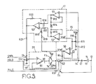
- the timing circuit l6 includes an oscillator 30.
- the oscillator comprises a type 3l40 operational amplifier 3l, the output of which is connected to its inverting-input through a diode Dl and a resistor R2.
- the output is also connected to the inverting input through a diode D2 and a preset resistor R3.
- the inverting input is connected through a capacitor C2 to the junction of a Zener diode ZDl and a resistor R4 which are connected in series between the positive supply rail and the earth line to provide a bias voltage.
- This junction is also connected through a resistor R5 and a resistor R6 to the output of amplifier 3l and the junction of these two resistors is connected to the non-inverting input.
- the non-inverting input is also connected to the earth rail through a switch S3 which may be closed to prevent oscillation.
- the oscillator 30 provides the basic timing signal of the pacemaker circuit and the resistor R3 may be adjusted to control the frequency of the stimulus pulses.
- the output of amplifier 3l is connected to the A input of a type 4528 monostable 32 which produces a signal TOUT at its Q output.
- the Q output of this monostable is connected to the input of a further type 4528 monostable 33 at the Q output of which is produced a signal PULS.
- the signal PULS is connected to the base of transistor Tl through a resistor R7.
- the monostable 33 is set to provide pulses having a variable duration.
- the Q output of monostable 32 is connected to one input of an OR gate 40, the output of which is connected to the enable inputs C D of a pair of monostables 4l and 42.
- the monostable 4l is set to produce pulses having a duration of 0.4ms and monostable 42 is set to produce pulses having a duration of 25 microseconds.
- the Q output of monostable 4l is connected to one input of an OR gate 43, the output of which is connected to the B input of monostable 42.
- the Q output of monostable 42 is connected to the B input of monostable 4l.
- the Q output of monostable 4l is also connected to the other input of OR gate 40 and the Q output of monostable 33 is connected to the other input of OR gate 43.
- the Q output of monostable 4l produces a signal HOLD and is connected to the control terminal of switch S2.
- the output of monostable 4l produces a signal SMPL which is connected to the control terminal of switch Sl.
- a waveform diagram is shown in Figure 5 for the signal appearing at the output of oscillator 30 and for the signals TOUT, PULS, SMPL, and HOLD.
- the signal TOUT controls the number of cycles of operation of switches Sl and S2. It may also be observed in Figure 5 that the switch Sl is always closed immediately upon termination of each stimulation pulse.
- the voltage reference source l5 comprises resistor Rl0, a potentiometer Rll and resistor Rl2 connected in series between the positive supply rail V DD and the earth line.
- the tapping on potentiometer Rll provides the reference voltage V ref .
- This junction is connected to the non-inverting input of a type 3l40 operational amplifier 50.
- the amplifier l7 comprises three type 3l40 operational amplifiers 5l, 52 and 53 which are connected as an instrumentation amplifier.
- the non-inverting input of amplifier 5l is connected to terminal l4 and the non-inverting input of amplifier 52 is connected to the tapping on potentiometer Rll.
- the output of amplifier 5l is connected through a resistor Rl3, a preset resistor Rl4 and l resistor Rl5 to the output of amplifier 52.
- the junction of resistors Rl3 and Rl4 is connected to the inverting input of amplifier 5l and the junction of resistors Rl4 and Rl5 is connected to the inverting input of amplifier 52.
- the output of amplifier 5l is connected through a resistor Rl6 to the inverting input of amplifier 53.
- the output of amplifier 52 is connected through a resistor Rl7, a potentiometer Rl8, and a resistor Rl9 to the output of amplifier 50 and the tapping on potentiometer Rl8 is connected to the non-inverting input of amplifier 53.
- the output of amplifier 53 is connected to its inverting input through resistor R20.
- the output of amplifier 53 represents the output of amplifier l7 and is connected through a resistor R2l and switch Sl to a capacitor C4 which represents the sample and hold circuit l9.
- the capacitor C4 is a low leakage polyester type capacitor. It is to be noted that the time constant of resistor R2l in capacitor C4 is 2.5 microseconds which is one tenth of the duration of the pulses of the signal SMPL.
- the amplifier 20 is formed from a type 3l40 operational amplifier 60 and a pair of transistors T3 and T4 connected between the positive supply line V DD and the negative supply line V ss .
- the emitters of transistors T3 and T4 are commonly connected to the inverting input of amplifier 60 to provide a voltage follower arrangement.
- the non-inverting input of amplifier 60 is connected to the junction of switch Sl and capacitor C4 and the emitters of transistors T3 and T4 are connected through the switch S2 to terminal l4.
- the lines between the non-inverting input of amplifier 5l and terminal l4 and the non-inverting input of amplifier 52 and the tapping on potentiometer Rll are screened and the entire circuit is enclosed in a die cast box which is earthed. It is also to be noted that the timing circuit l6 is arranged so that there are no logic level transitions during the sampling periods as such transitions could cause internal interference.
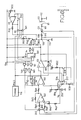
- FIG. 6 there is shown the circuit diagram of another pacemaker circuit.
- this pacemaker circuit the charge which is stored between the stimulating electrode and the myocardium during each stimulus pulse is measured by using an integrator and a measuring resistor and a substantially equal amount of charge is then removed upon termination of the stimulus pulse.
- the circuit shown in Figure 6 has a stimulating electrode lll and a reference electrode ll3.
- the electrode ll3 is connected to the earth line via a terminal ll2.
- the stimulating electrode lll is connected via a terminal ll0 and a capacitor Cll to a terminal ll4.
- Terminal ll4 is connected through a measuring resistor R30 to a terminal l30.
- the terminal l30 is connected to the earth line through the collector/ emitter path of a transistor Tll.
- the pacemaker circuit includes a timing circuit ll6 which provides a pulsed signal PULS similar to the signal PULS produced by the circuit shown in Figure 4.
- the signal PULS is supplied through a resistor R3l to the base of transistor Tll.
- the pacemaker circuit further includes a potentiometer R32 connected between the positive supply line V DD and the earth line. A tapping on potentiometer R32 provides a reference voltage V ref and this reference signal is supplied to the non-inverting input of a type 3l40 operational amplifier l3l.
- the output of amplifier l3l is connected through a resistor R33 to terminal l30.
- the output of amplifier l3l is also connected through an analog switch Sl0 to its non-inverting input. Its non-inverting input is also connected through an analog switch Sll to terminal l30 and an analog switch S9 is connected between the output of amplifier l3l and terminal l30.
- Terminal l30 is connected through an analog switch Sl2 and a resistor R40 to the inverting input of a type 3l40 operational amplifier l40.
- the terminal ll4 is connected through an analog switch Sl3, a resistor R4l, a potentiometer R42, and a resistor R43 to the junction of a Zener diode ZD2 and a resistor R44 connected in series between the positive supply line and the earth line.
- the resistor R44 and Zener diode ZD2 operate to provide a bias voltage V b .
- a tapping on potentiometer R42 is connected to the non-inverting input of amplifier l40 and its output is connected to its inverting input through a l megohm feed back resistor R45.
- operational amplifier l40 together with its associated components amplifies the voltage appearing across the measuring resistor R30.
- the output of operational amplifier l40 is connected through a resistor R46 to the inverting input of a type 3l40 operational amplifier l50.
- the non-inverting input of amplifier l50 receives the bias voltage V b .
- the output of amplifier l50 is connected through an integrating capacitor Cl3 to its inverting input.
- the output of amplifier l50 is also connected to its non-inverting input through a pair of analog switches Sl4 and Sl5, the junction of switches Sl4 and Sl5 being connected through a resistor to the earth line.
- amplifier l50 can integrate the current flowing through resistor R30 and so operate as an integrator. When the switches Sl4 and Sl5 are closed the integrator is reset.
- the output of amplifier l50 is connected to the positive input of a type 3ll comparator l5l.
- the junction of resistor R44 and Zener diode ZD2 is connected through a resistor R50 and the resistor R5l to the earth line.
- Resistor R50 is bridged by a pair of analog switches Sl6 and Sl7 and the junction of these switches is connected to the negative input of comparator l5l.
- a resistor R52 and a further analog switch Sl8 are connected between the positive supply line V DD and the earth line.
- the junction of resistor R52 and switch Sl8 is connected to the control terminal of switch Sl6.
- the control terminals of switches Sl7 and Sl8 are commonly connected together to the output of amplifier l5l.
- the signal PULS is connected through resistor R3l to the base of a transistor Tl2, the emitter of which is connected to the earth line and the collector of which is connected to the enable input (pin 6) of amplifier l5l.
- comparator l5l is connected through a resistor R53 and the resistor R54 to the positive supply rail V DD and the junction of these two resistors is connected to the base of a transistor Tl3.
- the emitter of transistor Tl3 is connected through a resistor R54 and a potiometer R55 to the positive supply line V DD and the collector of this transistor is connected to terminal l30.
- this transistor and the associated resistors operate as a current source.
- the output of amplifier l5l is connected to the A input of a type 4528 monostable l60.
- the Q output of this monostable is connected to the control terminal of switch Sll and the output is connected to the control terminal of switch Sl0.
- the Q output of monostable l60 is also connected to one input of a NAND gate l6l.
- NAND gate l6l is associated with another NAND gate l62, one input of which receives the signal PULS.
- the other input of NAND gates l6l and l62 are connected to the positive supply line V DD .
- NAND gate l6l is connected to one input of a NAND gate l63 and the output of NAND gate l62 is connected to one input of a NAND gate l64.
- the NAND gates l63 and l64 are connected as a R-S flip flop.
- the output of NAND gate l63 is connected to the control terminals of switches Sl3 and Sl4 and the output of NAND gate l64 is connected to the control terminals of switches Sl2 and Sl3.
- the current flowing through resistor R30 is integrated by amplifier l50 and the deviation of the output of this amplifier between the beginning and the end of the pulse represents the charge stored between electrodes lll and ll3.
- transistors Tll and Tl2 turn off and comparator l5l is enabled.
- the output of amplifier l50 is now below the bias voltage V b , the output of comparator l5l goes low thereby turning on transistor Tl3 which acts as a current source for removing the charge which has been stored.
- the current flowing through resistor R30 is again integrated by comparator l50.
- the charge stored between electrodes lll and ll3 is substantially removed by transistor Tl3.
- the charge is removed at this stage to an accuracy of approximately 0.l%. Because the interface between the stimulus electrode lll and the myocardium has complex non-linear properties, it is unlikely that this interface will be returned precisely to its initial state and it is for this reason that terminal l30 is then clamped for a preset period to the reference voltage V ref .
- the terminal l30 is supplied with a reference voltage via resistor R33, the intrinsic pulses in the heart may be sensed at terminal l30.
- the charge which is stored between the stimulus electrode and the myocardium during the stimulus pulse is subsequently removed thereby making it possible to detect the evoked heart pulses.
- the evoked pulses may therefore be used for diagnosis whilst the pacemaker circuit is operating.
- damaged tissue in a heart may cause a secondary wave to follow the due PRST waves and this wave may be detected using the present invention.
- the pacemaker circuit of the present invention may be modified so that it can detect a specific component of the evoked pulse and use this to modify the operation of the pacemaker circuit.
- the detection of such a pulse may be used to modify the frequency or intensity of the stimulus pulses or to suppress or trigger them as may be appropriate.
Landscapes
- Health & Medical Sciences (AREA)
- Cardiology (AREA)
- Heart & Thoracic Surgery (AREA)
- Engineering & Computer Science (AREA)
- Biomedical Technology (AREA)
- Nuclear Medicine, Radiotherapy & Molecular Imaging (AREA)
- Radiology & Medical Imaging (AREA)
- Life Sciences & Earth Sciences (AREA)
- Animal Behavior & Ethology (AREA)
- General Health & Medical Sciences (AREA)
- Public Health (AREA)
- Veterinary Medicine (AREA)
- Electrotherapy Devices (AREA)
Applications Claiming Priority (2)
| Application Number | Priority Date | Filing Date | Title |
|---|---|---|---|
| GB8612659 | 1986-05-23 | ||
| GB868612659A GB8612659D0 (en) | 1986-05-23 | 1986-05-23 | Cardiac pacemaker circuit |
Publications (2)
| Publication Number | Publication Date |
|---|---|
| EP0246908A2 true EP0246908A2 (de) | 1987-11-25 |
| EP0246908A3 EP0246908A3 (de) | 1989-11-02 |
Family
ID=10598373
Family Applications (1)
| Application Number | Title | Priority Date | Filing Date |
|---|---|---|---|
| EP87304556A Withdrawn EP0246908A3 (de) | 1986-05-23 | 1987-05-21 | Schaltung für Herzschrittmacher |
Country Status (3)
| Country | Link |
|---|---|
| US (1) | US4811738A (de) |
| EP (1) | EP0246908A3 (de) |
| GB (1) | GB8612659D0 (de) |
Cited By (1)
| Publication number | Priority date | Publication date | Assignee | Title |
|---|---|---|---|---|
| WO1992019319A1 (en) * | 1991-05-06 | 1992-11-12 | Intermedics, Inc. | Apparatus and method for an implanted cardiac pacemaker with multiuse electrode with potential restoration |
Families Citing this family (16)
| Publication number | Priority date | Publication date | Assignee | Title |
|---|---|---|---|---|
| US4949720A (en) * | 1988-09-20 | 1990-08-21 | Medtronic, Inc. | Apparatus for measuring the lead current in a pacemaker |
| US4964406A (en) * | 1989-05-19 | 1990-10-23 | Ventritex, Inc. | Implantable cardiac defibrillator employing a switched capacitor stage having a non-50/50 duty cycle |
| US5233985A (en) * | 1990-08-10 | 1993-08-10 | Medtronic, Inc. | Cardiac pacemaker with operational amplifier output circuit |
| SE9303121D0 (sv) * | 1993-09-24 | 1993-09-24 | Siemens Elema Ab | Hjärtstimulator |
| US5861013A (en) * | 1997-04-29 | 1999-01-19 | Medtronic Inc. | Peak tracking capture detection circuit and method |
| US5873898A (en) * | 1997-04-29 | 1999-02-23 | Medtronic, Inc. | Microprocessor capture detection circuit and method |
| US6185450B1 (en) | 1998-01-26 | 2001-02-06 | Physio-Control Manufacturing Corporation | Digital sliding pole fast-restore for an electrocardiograph display |
| SE9800407D0 (sv) * | 1998-02-12 | 1998-02-12 | Pacesetter Ab | Heart stimulator |
| US5954756A (en) * | 1998-04-09 | 1999-09-21 | Medtronic, Inc. | Microprocessor capture detection circuit and method |
| US6711437B2 (en) | 2001-07-30 | 2004-03-23 | Medtronic, Inc. | Pacing channel isolation in multi-site cardiac pacing systems |
| US8340762B2 (en) * | 2003-04-23 | 2012-12-25 | Medtronic, Inc. | Pulse generation techniques for implantable pulse generator systems |
| US9008787B2 (en) * | 2007-10-12 | 2015-04-14 | Cochlear Limited | Active electrode state control system |
| US8588928B2 (en) * | 2007-10-12 | 2013-11-19 | Cochlear Limited | Active electrode state control system with current compensation to reduce residual DC/LF voltage |
| US11040202B2 (en) * | 2018-03-30 | 2021-06-22 | Boston Scientific Neuromodulation Corporation | Circuitry to assist with neural sensing in an implantable stimulator device |
| US11147973B2 (en) * | 2019-04-07 | 2021-10-19 | Amirkabir University of Technology | Charge-balanced current-controlled stimulation |
| WO2023076904A1 (en) | 2021-10-29 | 2023-05-04 | Boston Scientific Neuromodulation Corporation | Stimulation circuitry in an implantable stimulator device for providing a tissue voltage as useful during neural response sensing |
Family Cites Families (9)
| Publication number | Priority date | Publication date | Assignee | Title |
|---|---|---|---|---|
| US3635224A (en) * | 1970-02-10 | 1972-01-18 | American Optical Corp | Safe rate pacer |
| US3835865A (en) * | 1970-07-10 | 1974-09-17 | Gen Electric | Body organ stimulator |
| CA964334A (en) * | 1970-07-10 | 1975-03-11 | General Electric Company | Body organ stimulator |
| IL42784A (en) * | 1972-08-09 | 1975-12-31 | Greatbatch W Ltd | Constant energy pulse generator |
| US4170999A (en) * | 1977-08-19 | 1979-10-16 | Biotronik Mess- Und Therapiegerate Gmbh & Co. | Demand pacer having reduced recovery time |
| EP0000989B1 (de) * | 1977-08-19 | 1981-11-25 | BIOTRONIK Mess- und Therapiegeräte GmbH & Co Ingenieurbüro Berlin | Bedarfschrittmacher mit einer verminderten Erholungszeit |
| US4343312A (en) * | 1979-04-16 | 1982-08-10 | Vitafin N.V. | Pacemaker output circuit |
| DE2939173A1 (de) * | 1979-09-27 | 1981-04-16 | Siemens AG, 1000 Berlin und 8000 München | Herzschrittmacher |
| US4399818A (en) * | 1981-04-06 | 1983-08-23 | Telectronics Pty. Ltd. | Direct-coupled output stage for rapid-signal biological stimulator |
-
1986
- 1986-05-23 GB GB868612659A patent/GB8612659D0/en active Pending
-
1987
- 1987-05-21 US US07/053,135 patent/US4811738A/en not_active Expired - Fee Related
- 1987-05-21 EP EP87304556A patent/EP0246908A3/de not_active Withdrawn
Cited By (2)
| Publication number | Priority date | Publication date | Assignee | Title |
|---|---|---|---|---|
| WO1992019319A1 (en) * | 1991-05-06 | 1992-11-12 | Intermedics, Inc. | Apparatus and method for an implanted cardiac pacemaker with multiuse electrode with potential restoration |
| US5228437A (en) * | 1991-05-06 | 1993-07-20 | Intermedics Orthopedics, Inc. | Cardiac pacemaker and method for detecting cardiac signals |
Also Published As
| Publication number | Publication date |
|---|---|
| US4811738A (en) | 1989-03-14 |
| EP0246908A3 (de) | 1989-11-02 |
| GB8612659D0 (en) | 1986-07-02 |
Similar Documents
| Publication | Publication Date | Title |
|---|---|---|
| EP0246908A2 (de) | Schaltung für Herzschrittmacher | |
| CA1098173A (en) | Pacemaker artifact suppression in coronary monitoring | |
| US4537201A (en) | Process and device for detecting the response of the heart to an electrical stimulation pulse | |
| US4821724A (en) | Pacing pulse compensation | |
| US5443485A (en) | Apparatus and method for capture detection in a cardiac stimulator | |
| US4539999A (en) | Method and device for subtracting a pacer signal from an ECG signal | |
| US4903700A (en) | Pacing pulse compensation | |
| Irnich et al. | Electromagnetic interference in implantable pacemakers | |
| DE68922676T2 (de) | Verfahren und Apparat zur Sicherstellung, dass die Programmierung eines Schrittmachers mit der angeschlossenen Elektrodenleitung kompatibel ist. | |
| CA1316987C (en) | Method and apparatus for measuring the lead current in a pacemaker | |
| US4649931A (en) | Sampled data sense amplifier | |
| US3756246A (en) | Apparatus for externally determining actual output of an implanted energy source | |
| US4099530A (en) | Cardiac pacer circuitry to facilitate testing of patient heart activity and pacer pulses | |
| IL34424A (en) | An electrocardiographic monitoring system | |
| DE60109117D1 (de) | Vorrichtung zur Messung der komplexen Impedanz einer Sonde, einer aktiven implantierbaren medizinischen Vorrichtung, insbesondere eines Herzschrittmacher, Defibrillator, und/oder Kardiovertierer | |
| Johnson et al. | Investigations of the electrical properties of cardiac muscle fibres with the aid of intracellular double-barrelled electrodes | |
| DE2755702A1 (de) | Implantierbarer herzschrittmacher | |
| US4448196A (en) | Delta modulator for measuring voltage levels in a heart pacer | |
| EP0148312A3 (de) | Scahltungsanordnung zum Überprüfen der Lage von Elektroden | |
| US4574813A (en) | Pace pulse signal conditioning circuit | |
| DE2619001A1 (de) | Herzschrittmacher | |
| CA1057359A (en) | Demand cardiac pacemaker with input circuit portion of increased sensitivity | |
| DE1762069C3 (de) | Sperrschwinger-Schaltungsanordnung für eine Überwachung eines Torimpulsgenerators. Ausscheidung aus: 1290182 | |
| DE2659115A1 (de) | Magnetimpulsgeraet und seine medizinische anwendung | |
| DE69217932T2 (de) | Verfahren und vorrichtung zum messen und wiederherstellen des elektrischen potentials einer elektrode |
Legal Events
| Date | Code | Title | Description |
|---|---|---|---|
| PUAI | Public reference made under article 153(3) epc to a published international application that has entered the european phase |
Free format text: ORIGINAL CODE: 0009012 |
|
| AK | Designated contracting states |
Kind code of ref document: A2 Designated state(s): AT BE CH DE ES FR GB GR IT LI LU NL SE |
|
| PUAL | Search report despatched |
Free format text: ORIGINAL CODE: 0009013 |
|
| AK | Designated contracting states |
Kind code of ref document: A3 Designated state(s): AT BE CH DE ES FR GB GR IT LI LU NL SE |
|
| 17P | Request for examination filed |
Effective date: 19900226 |
|
| STAA | Information on the status of an ep patent application or granted ep patent |
Free format text: STATUS: THE APPLICATION IS DEEMED TO BE WITHDRAWN |
|
| 18D | Application deemed to be withdrawn |
Effective date: 19911203 |
|
| RIN1 | Information on inventor provided before grant (corrected) |
Inventor name: ECONOMIDES, APOLLO PLATO Inventor name: GERGELY, STEPHEN Inventor name: WALTON, CHRISTOPHER |