EP0246689A2 - Circuit for converting three-state signals into binary signals - Google Patents
Circuit for converting three-state signals into binary signals Download PDFInfo
- Publication number
- EP0246689A2 EP0246689A2 EP87200843A EP87200843A EP0246689A2 EP 0246689 A2 EP0246689 A2 EP 0246689A2 EP 87200843 A EP87200843 A EP 87200843A EP 87200843 A EP87200843 A EP 87200843A EP 0246689 A2 EP0246689 A2 EP 0246689A2
- Authority
- EP
- European Patent Office
- Prior art keywords
- current
- output
- transistor
- input
- diode path
- Prior art date
- Legal status (The legal status is an assumption and is not a legal conclusion. Google has not performed a legal analysis and makes no representation as to the accuracy of the status listed.)
- Granted
Links
Images

Classifications
-
- H—ELECTRICITY
- H03—ELECTRONIC CIRCUITRY
- H03M—CODING; DECODING; CODE CONVERSION IN GENERAL
- H03M5/00—Conversion of the form of the representation of individual digits
- H03M5/02—Conversion to or from representation by pulses
- H03M5/16—Conversion to or from representation by pulses the pulses having three levels
Definitions
- the invention relates to a circuit arrangement for converting three-state signals into binary signals.
- a reference voltage range is defined by means of one or more ohmic voltage dividers, which lies between the potential of the positive and the negative supply voltage source.
- the object of the present invention is to create a circuit arrangement of the type mentioned at the outset without an ohmic voltage divider.
- a first direct current source connected on one side to the negative supply voltage connection and a second direct current source connected on one side to the positive supply voltage connection of a supply voltage source is provided and that the direct current sources with their free connection via a first or a second diode path with a common input and Via a third or fourth diode path, which are identical to the first or second diode path, are connected to a first or a second output transistor providing an output signal.
- the diode paths can consist of one or more diode elements connected in series and in the forward direction. If the potential at the common input is positive, the current of the first current source flows via the first diode path to the common input and no current is supplied to the output transistor coupled to the third diode path. In contrast, the current of the second current source in this case flows via the fourth diode path to the output transistor coupled to it.
- the current from the second current source flows via the second diode path to the common input.
- the fourth diode path remains currentless and no current is supplied to the output transistor coupled to it.
- the current supplied by the first current source flows via the third diode path to the output transistor coupled to it.
- the current of the two current sources only flows via the third and fourth diode paths to the two output transistors.
- the third or fourth diode path were connected directly to the input, for example the base of the associated output transistor, these transistors must have the opposite conductivity type and be connected to opposite supply voltage terminals.
- the potentials occurring at their outputs, in particular their collectors, which represent the binary output signals, would then depend on the level of the supply voltage. According to a further development of the invention, this can be avoided in that one of the third and fourth diode sections is direct and the other another is connected via a current mirror to the first or second output transistor and that the two output transistors are connected in the same way.
- the output transistors can then be connected to the same conductivity type and to the same supply voltage terminal.
- the further development of the invention provides that a switching transistor is connected in parallel to the input of at least one of the output transistors, which switching transistor can be controlled by the output current of a current mirror, the input current of which is via the first or the second diode path is flowing current.
- the input of an output transistor is short-circuited by the switching transistor connected in parallel, so that any residual currents are kept away from the output transistor.
- a preferred development of the invention provides that the transistors contained in the circuit, the emitters of which are connected to the negative supply voltage connection, are designed in I 2 L circuit technology and that the base current of these transistors is supplied by a common injector. With this configuration, crystal area can be saved when manufacturing the circuit using integrated circuit technology, and the currents of the current sources which are supplied by the injector can be relatively small.
- first direct current source S1 which has one connection to the negative supply voltage terminal, which is connected to ground
- second direct current source S2 which has one connection to the positive supply voltage terminal of a supply voltage source U.
- the respective other connection of the first and the second direct current source which supply a direct current of, for example, 1 pA, is connected via a first or a second diode path D1 or D2 to a common input, to which the three-state signal to be implemented is present .
- the free connection of the current sources S1 and S2 is also via a third diode path D3, which is identical to the first diode path Dl, or via a fourth diode path, which is identical to the second diode path, to the base terminal of a pnp output transistor Tp or an npn output transistor Tn, whose emitter is connected to the positive or negative supply voltage terminal and whose collector forms the output P or N of the circuit.
- An evaluation circuit is preferably connected to the outputs P and N, preferably using I 2 L circuit technology, which processes the binary output signals occurring on these signals.
- the common input I is connected to a switch Sw with three switch contacts, so that, depending on the position of the switch, the common input is either not connected or is connected to ground or the positive supply voltage.
- the bias voltage of the diode path D4 in the forward direction becomes greater than the corresponding voltage at the diode path D2.
- the current of the current source S2 then flows into the base of the transistor Tn and as a result appears at the output N.
- the output transistor Tp remains conductive as long as only the potential at the input I remains more negative than the base potential of the output transistor Tp.
- both output transistors carry an output current.
- input I remains unconnected, because then no current can flow through input I.
- a current flow from the current source S2 via the diode paths D2 and Dl to the current source S1 is excluded if the supply voltage U is greater than the sum of the base-emitter voltage of an output transistor, the forward voltage of one of the diode paths D3 or D4 and the Operating voltage of the current source S1 or S2.
- the first current source S1 is formed by the collector-emitter path of an npn transistor T21, the emitter of which is connected to the negative supply voltage terminal and the collector of which is connected to the first and the third diode path.
- the first diode path is formed by the series connection of an npn transistor T17 which acts as a diode by connecting its collector to its base and a pnp transistor T15 which is likewise connected as a diode.
- the third diode path is constructed in the same way and consists of the series connection of the npn or pnp transistors Tl8 and T16 connected as diodes.
- the current source S2 is formed by the collector-emitter path of a transistor T3, the emitter of which is connected to the positive supply voltage terminal and the collector of which is connected to the second or fourth diode path.
- the second diode path is formed by the npn transistors T7 and T9 connected as a diode and the fourth diode path by the transistors T8 and Tll connected as a diode.
- a transistor T13 the base of which is connected to the second current source T3 via the fourth diode path T8, Tll and whose emitter is connected to ground, corresponds in function to the output transistor Tn.
- the third diode path is not connected directly to the base of the npn output transistor T23, whose emitter is connected to the negative supply voltage terminal, but to the input of one through the Transistors T5 and T6 formed current mirror, the output of which is connected to the base of transistor T23. Switching on the current mirror T5, T6 has the advantage that transistors of the same conductivity type can be used as output transistors.
- the first current source T21 is formed by an output of a current mirror, the input of which is an npn transistor T19 connected as a diode and the other output of which is a transistor T20, the base-emitter path of which is connected in parallel to the base-emitter path of the transistor T21.
- the collector of transistor T20 is connected to a pnp transistor T4 connected as a diode, the emitter of which is connected to the positive supply voltage terminal and which, together with transistor T3, forms a current mirror. Therefore, the current of the current source T3 is the same as the current of the current source T21.
- the input current of the current mirror T19, T20, T21 is supplied by a current source Q and has a size of e.g. 1 uA.
- the collector-emitter path of a transistor T12 or T22 is connected in parallel to the base-emitter paths of these transistors.
- the transistor T12 is fed by the output of a current mirror Tl, T2, the input of which is connected to the output of a further current mirror, the one transistor T10 and the transistor T9 connected as a diode which is connected to the heard second diode path includes.
- the transistor T22 is controlled by the collector current of a transistor T14 which, together with the transistor T15 of the first diode path connected as a diode, forms a current mirror.
- the output of the associated current mirror supplies a current which makes the transistor T22 or T12 conductive and short-circuits the input of the output transistor T13 or T23.
- the npn transistors T12, T13 and T19 ... T23, whose emitters are connected to the negative supply voltage terminal or ground, are advantageously implemented using I 2 L circuit technology.
- the current source Q can then be formed by a so-called injector transistor, which is suitable for generating small enough currents with a small crystal area, in particular if it is still used to supply 2L gates, which is part of a further circuit which is connected to the in Fig. 3 circuit shown is mounted on the same semiconductor substrate.
- the supply voltage of the circuit shown in FIG. 3 need only be three times the base-emitter voltage of one of the transistors plus the collector-emitter saturation voltage; if the transistors T7, T8 and T17, T18 connected as diodes are omitted, the supply voltage can be even lower by a base-emitter voltage and the switching can be even simpler with otherwise unchanged properties.
- the circuit can process not only stationary signals as provided by the circuit Sw in Fig. 1, but also AC signals.
Landscapes
- Engineering & Computer Science (AREA)
- Theoretical Computer Science (AREA)
- Logic Circuits (AREA)
- Amplifiers (AREA)
- Electronic Switches (AREA)
Abstract
Die Erfindung betrifft eine Schaltung, die Drei-Zustands-Signale in binäre Signale umsetzt. Sie enthält zwei Stromquellen, die über je eine Diodenstrecke mit einem gemeinsamen Eingang und über je eine weitere Diodenstrecke mit je einem Ausgangstransistor verbunden sind. Je nach Potential am Eingang führt einer der beiden Ausgangstransistoren oder beide Ausgangstransistoren einen Ausgangsgleichstrom.The invention relates to a circuit which converts three-state signals into binary signals. It contains two current sources, each of which is connected to a common input via a diode path and to an output transistor each via a further diode path. Depending on the potential at the input, one of the two output transistors or both output transistors carry an output direct current.
Description
Die Erfindung bezieht sich auf eine Schaltungsanordnung zum Umsetzen von Drei-Zustands-Signalen in binäre Signale. Bei bekannten Schaltungen dieser Art wird mittels eines oder mehrerer ohmscher Spannungsteiler ein Referenz-Spannungsbereich definiert, der zwischen dem Potential der positiven und der negativen Versorgungsspannungsquelle liegt.The invention relates to a circuit arrangement for converting three-state signals into binary signals. In known circuits of this type, a reference voltage range is defined by means of one or more ohmic voltage dividers, which lies between the potential of the positive and the negative supply voltage source.
Wenn der Stromverbrauch einer solchen Schaltung gering sein soll, müssen hochohmige Spannungsteiler verwendet werden, die sich schlecht in integrierter Schaltungstechnik herstellen lassen.If the current consumption of such a circuit should be low, high-resistance voltage dividers must be used, which are difficult to manufacture in integrated circuit technology.
Aufgabe der vorliegenden eRfindung ist es, eine Schaltungsanordnung der eingangs genannten Art ohne ohmsche Spannungsteiler zu schaffen.The object of the present invention is to create a circuit arrangement of the type mentioned at the outset without an ohmic voltage divider.
Diese Aufgabe wird erfindungsgemäß dadurch gelöst, daß eine erste einseitig mit dem negativen Versorgungsspannungsanschluß und eine zweite einseitig mit dem positiven Versorgungsspannungsanschluß einer Versorgungsspannungsquelle verbundene Gleichstromquelle vorgesehen ist und daß die Gleichstromquellen mit ihrem freien Anschluß über eine erste bzw. eine zweite Diodenstrecke mit einem gemeinsamen Eingang und über eine dritte bzw. vierte Diodenstrecke, die zur ersten bzw. zweiten Diodenstrecke gleichartig sind, mit einem ersten bzw. einem zweiten ein Ausgangssignal liefernden Ausgangstransistor verbunden sind.This object is achieved in that a first direct current source connected on one side to the negative supply voltage connection and a second direct current source connected on one side to the positive supply voltage connection of a supply voltage source is provided and that the direct current sources with their free connection via a first or a second diode path with a common input and Via a third or fourth diode path, which are identical to the first or second diode path, are connected to a first or a second output transistor providing an output signal.
Die Diodenstrecken können dabei aus einem oder mehrere in Serie und in Durchlaßrichtung geschalteten Diodenelementen bestehen. Wenn das Potential am gemeinsamen Eingang positiv ist, fließt der Strom der ersten Stromquelle über die erste Diodenstrecke zum gemeinsamen Eingang und dem mit der dritten Diodenstrecke gekoppelten Ausgangstransistor wird kein Strom zugeführt. Hingegen fließt der Strom der zweiten Stromquelle in diesem Fall über die vierte Diodenstrecke zu dem damit gekoppelten Ausgangstransistor.The diode paths can consist of one or more diode elements connected in series and in the forward direction. If the potential at the common input is positive, the current of the first current source flows via the first diode path to the common input and no current is supplied to the output transistor coupled to the third diode path. In contrast, the current of the second current source in this case flows via the fourth diode path to the output transistor coupled to it.
Wird hingegen das Potential am gemeinsamen Eingang genügend negativ, dann fließt der Strom der zweiten Stromquelle über die zweite Diodenstrecke zum gemeinsamen Eingang. Die vierte Diodenstrecke bleibt stromlos und dem damit gekoppelten Ausgangstransistor wird kein Strom zugeführt. Dafür fließt der von der ersten Stromquelle gelieferte Strom über die dritte Diodenstrecke zu dem damit gekoppelten Ausgangstransistor.If, on the other hand, the potential at the common input becomes sufficiently negative, then the current from the second current source flows via the second diode path to the common input. The fourth diode path remains currentless and no current is supplied to the output transistor coupled to it. For this purpose, the current supplied by the first current source flows via the third diode path to the output transistor coupled to it.
In einem Zwischenbereich fließt der Strom der beiden Stromquellen nur über die dritte und die vierte-Diodenstrecke zu den beiden Ausgangstransistoren.In an intermediate area, the current of the two current sources only flows via the third and fourth diode paths to the two output transistors.
Wenn die dritte bzw. die vierte Diodenstrecke direkt mit dem Eingang, z.B. der Basis des zugehörigen Ausgangstransistors, verbunden wären, müssen diese Transistoren den entgegengesetzten Leitfähigkeitstyp aufweisen und mit entgegengesetzten Versorgungsspannungsklemmen verbunden sein. Die an ihren Ausgängen, insbesondere ihren Kollektoren, auftretenden Potentiale, die die binären Ausgangssignale darstellen, würden dann von der Höhe der Versorgungsspannung abhängig sein. Dies läßt sich nach einer Weiterbildung der Erfindung dadurch vermeiden, daß von der dritten und vierten Diodenstrecke die eine direkt und die andere über einen Stromspiegel mit dem ersten bzw. zweiten Ausgangstransistor verbunden ist und daß die beiden Ausgangstransistoren gleichartig geschaltet sind. Die Ausgangstransistoren können dann vom gleichen Leitfähigkeitstyp und mit der gleichen Versorgungsspannungsklemme verbunden sein.If the third or fourth diode path were connected directly to the input, for example the base of the associated output transistor, these transistors must have the opposite conductivity type and be connected to opposite supply voltage terminals. The potentials occurring at their outputs, in particular their collectors, which represent the binary output signals, would then depend on the level of the supply voltage. According to a further development of the invention, this can be avoided in that one of the third and fourth diode sections is direct and the other another is connected via a current mirror to the first or second output transistor and that the two output transistors are connected in the same way. The output transistors can then be connected to the same conductivity type and to the same supply voltage terminal.
Wenn über die dritte bzw. die vierte Diodenstrecke kein Strom fließt, wird den Basen der Ausgangstransistoren von den Stromquellen kein Strom zugeführt, so daß sie gesperrt sind. Um eine sichere Sperrung zu erreichen und einen definierten Übergang vom leitenden in den gesperrten Zustand, ist in der Weiterbildung der Erfindung vorgesehen, daß dem Eingang wenigstens eines der Ausgangstransistoren ein Schalttransistor parallelgeschaltet ist, der durch den Ausgangsstrom eines Stromspiegels steuerbar ist, dessen Eingangsstrom der über die erste bzw. die zweite Diodenstrecke fliessende Strom ist. Der Eingang eines Ausgangstransistor wird dabei durch den parallelgeschalteten Schalttransistor kurzgeschlossen, so daß etwaige Restströme vom Ausgangstransistor ferngehalten werden.If no current flows through the third or fourth diode path, no current is supplied to the bases of the output transistors from the current sources, so that they are blocked. In order to achieve a safe blocking and a defined transition from the conductive to the blocked state, the further development of the invention provides that a switching transistor is connected in parallel to the input of at least one of the output transistors, which switching transistor can be controlled by the output current of a current mirror, the input current of which is via the first or the second diode path is flowing current. The input of an output transistor is short-circuited by the switching transistor connected in parallel, so that any residual currents are kept away from the output transistor.
Eine bevorzugte Weiterbildung der Erfindung sieht vor, daß die in der Schaltung enthaltenen Transistoren, deren Emitter mit dem negativen Versorgungsspannungsanschluß verbunden sind, in I2L-Schaltungstechnik ausgebildet sind und daß der Basisstrom dieser Transistoren von einem gemeinsamen Injektor geliefert wird. Bei dieser Ausgestaltung kann bei Herstellung der Schaltung in integrierter Schaltungstechnik Kristallfläche eingespart werden und die Ströme der Stromquellen, die von dem Injektor geliefert werden, können relativ klein sein.A preferred development of the invention provides that the transistors contained in the circuit, the emitters of which are connected to the negative supply voltage connection, are designed in I 2 L circuit technology and that the base current of these transistors is supplied by a common injector. With this configuration, crystal area can be saved when manufacturing the circuit using integrated circuit technology, and the currents of the current sources which are supplied by the injector can be relatively small.
Die Erfindung wird nachstehend anhand der Zeichnung näher erläutert. Es zeigen:
- Fig. 1 ein vereinfachtes Prinzipschaltbild einer erfindungsgemäßen Schaltung,
- Fig. 2a und 2b den Verlauf der Ströme der Ausgangstransistoren als Funktion der Eingangsspannung, und
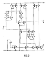
- Fig. 3 das Schaltbild einer bevorzugten Ausführungsform nach der Erfindung.
- 1 is a simplified schematic diagram of a circuit according to the invention,
- 2a and 2b the course of the currents of the output transistors as a function of the input voltage, and
- Fig. 3 shows the circuit diagram of a preferred embodiment according to the invention.
Die Fig. 1 enthält eine erste Gleichstromquelle Sl, die mit ihrem einen Anschluß an die negative, mit Masse verbundene Versorgungsspannungsklemme und eine zweite Gleichstromquelle S2, die mit ihrem einen Anschluß an die positive Versorgungsspannungsklemme einer Versorgungsspannungsquelle U angeschlossen ist. Der jeweils andere Anschluß der ersten bzw. der zweiten Gleichstromquelle, die einen Gleichstrom von z.B. 1 pA liefern, ist über eine erste bzw. eine zweite Diodenstrecke Dl bzw. D2 mit einem gemeinsamen Eingang verbunden, an dem das umzusetzende Drei-Zustands-Signal anliegt. Der freie Anschluß der Stromquellen Sl bzw. S2 ist darüber hinaus über eine dritte Diodenstrecke D3, die mit der ersten Diodenstrecke Dl gleichartig ist, bzw. über eine vierte Diodenstrecke, die mit der zweiten Diodenstrecke gleichartig ist, mit dem Basisanschluß eines pnp-Ausgangstransistors Tp bzw. eines npn-Ausgangstransistors Tn verbunden, dessen Emitter mit der positiven bzw. negativen Versorgungsspannungsklemme verbunden ist und dessen Kollektor den Ausgang P bzw. N der Schaltung bildet. An die Ausgänge P und N ist eine nicht näher dargestellte Auswerteschaltung, vorzugsweise in I2L-Schaltungstechnik angeschlossen, die die an diesen Signalen auftretenden binären Ausgangssignale verarbeitet.1 contains a first direct current source S1, which has one connection to the negative supply voltage terminal, which is connected to ground, and a second direct current source S2, which has one connection to the positive supply voltage terminal of a supply voltage source U. The respective other connection of the first and the second direct current source, which supply a direct current of, for example, 1 pA, is connected via a first or a second diode path D1 or D2 to a common input, to which the three-state signal to be implemented is present . The free connection of the current sources S1 and S2 is also via a third diode path D3, which is identical to the first diode path Dl, or via a fourth diode path, which is identical to the second diode path, to the base terminal of a pnp output transistor Tp or an npn output transistor Tn, whose emitter is connected to the positive or negative supply voltage terminal and whose collector forms the output P or N of the circuit. An evaluation circuit, not shown, is preferably connected to the outputs P and N, preferably using I 2 L circuit technology, which processes the binary output signals occurring on these signals.
Der gemeinsame Eingang I ist an einen Schalter Sw mit drei Schaltkontakten angeschlossen, so daß je nach Stellung des Schalters der gemeinsame Eingang entweder unbeschaltet ist oder mit Masse oder der positiven Speisespannung verbunden ist.The common input I is connected to a switch Sw with three switch contacts, so that, depending on the position of the switch, the common input is either not connected or is connected to ground or the positive supply voltage.
In den Fig. 2a und 2b ist der Verlauf der Ausgangsströme In und Ip der Ausgangstransistoren Tn und Tp als Funktion der Spannung Ui am gemeinsamen Eingang I angegeben. Wenn die Spannung am gemeinsamen Eingang Null Volt beträgt oder zumindest kleiner ist als die Emitter-Basis-Spannung u des Transistors Tn, dann ist die Vorspannung der Diodenstrecke D2 in Flußrichtung größer als die entsprechende Vorspannung der Diodenstrecke D4. Deshalb fließt praktisch der gesamte Strom der Stromquelle S2 über die Diodenstrecke D2 zum Eingang I. Der Transistor Tn erhält keinen Basisstrom, so daß der Strom In am Ausgang N praktisch Null ist. - Auf der anderen Seite ist - bei Massepotential am Eingang I - die Diodenstrecke D3 leitend und die Diodenstrecke Dl gesperrt. Der gesamte Strom der Stromquelle S1 fließt also über die Diodenstrecke D3 in die Basis des Transistors Tp, so daß am Ausgang P ein Strom Ip fließt, nämlich der Kollektorstrom des Transistors Tp.2a and 2b show the course of the output currents In and Ip of the output transistors Tn and Tp as a function of the voltage Ui at the common input I. If the voltage at the common input is zero volts or at least less than the emitter-base voltage u of the transistor Tn, then the bias of the diode path D2 in the forward direction is greater than the corresponding bias of the diode path D4. Therefore, practically all of the current of the current source S2 flows through the diode path D2 to the input I. The transistor Tn receives no base current, so that the current In at the output N is practically zero. - On the other hand - at ground potential at input I - the diode path D3 is conductive and the diode path Dl is blocked. The entire current of the current source S1 thus flows via the diode path D3 into the base of the transistor Tp, so that a current Ip flows at the output P, namely the collector current of the transistor Tp.
An dem beschriebenen Zustand ändert sich nichts, solange die Spannung an dem Eingang I unterhalb der Basis-Emitter-Spannung des Transistors Tn bleibt.Nothing changes in the described state as long as the voltage at input I remains below the base-emitter voltage of transistor Tn.
Wenn die Spannung an dem Eingang I die Basis-Emitter-Spannung u des Transistors Tn überschreitet, wird die Vorspannung der Diodenstrecke D4 in Flußrichtung größer als die entsprechende Spannung an der Diodenstrecke D2. Der Strom der Stromquelle S2 fließt dann in die Basis des Transistors Tn und als Folge erscheint am Ausgang N ein Strom In - der Kollektorstrom des Transistors Tn. Der Ausgangstransistor Tp bleibt unverändert leitend, solange nur das Potential am Eingang I negativer bleibt als das Basispotential des Ausgangstransistor Tp.If the voltage at the input I exceeds the base-emitter voltage u of the transistor Tn, the bias voltage of the diode path D4 in the forward direction becomes greater than the corresponding voltage at the diode path D2. The current of the current source S2 then flows into the base of the transistor Tn and as a result appears at the output N. Current In - the collector current of the transistor Tn. The output transistor Tp remains conductive as long as only the potential at the input I remains more negative than the base potential of the output transistor Tp.
In diesem Zustand führen also beide Ausgangstransistoren einen Ausgangsstrom. Das gleiche gilt auch, wenn der Eingang I unbeschaltet bleibt, weil dann kein Strom über den Eingang I fließen kann. Auch ein Stromfluß von der Stromquelle S2 über die Diodenstrecken D2 und Dl zur Stromquelle Sl ist ausgeschlossen, wenn die Versorgungsspannung U größer ist als die Summe aus der Basis-Emitter-Spannung eines Ausgangstransistors, aus der Vorwärtsspannung einer der Diodenstrecken D3 oder D4 und aus der Betriebsspannung der Stromquelle Sl oder S2.In this state, both output transistors carry an output current. The same also applies if input I remains unconnected, because then no current can flow through input I. A current flow from the current source S2 via the diode paths D2 and Dl to the current source S1 is excluded if the supply voltage U is greater than the sum of the base-emitter voltage of an output transistor, the forward voltage of one of the diode paths D3 or D4 and the Operating voltage of the current source S1 or S2.
Wenn die Spannung Ui am Eingang I positiver wird als die Spannung an der Basis des Transistors Tp (gegenüber Masse), dann fließt der Strom der Stromquelle Sl über die Diodenstrecke Dl und der Ausgangstransistor Tp wird stromlos, d.h. der Ausgangsstrom Ip wird Null. - Der Strom der Stromquelle S2 fließt in diesem Zustand weiterhin über die Diodenstrecke D4 in den Eingang des Transistors Tn, so daß ein Ausgangsstrom In fließt; über die Diodenstrecke D2 fließt kein Strom.If the voltage Ui at the input I becomes more positive than the voltage at the base of the transistor Tp (with respect to ground), then the current from the current source S1 flows through the diode path Dl and the output transistor Tp becomes currentless, i.e. the output current Ip becomes zero. - In this state, the current of the current source S2 continues to flow via the diode path D4 into the input of the transistor Tn, so that an output current In flows; No current flows through the diode path D2.
Ein Drei-Zustands-Signal am Eingang I wird durch die in Fig. 1 dargestellte Schaltung also wie folgt in ein binäres Signal an den Ausgängen N und P umgesetzt:
- a) Im Eingangs-Spannungsbereich 0 C Ui < u führt der Ausgangstransistor Tn keinen Ausgangsstrom und der Ausgangstransistor Tp führt Strom.
- b) Im Eingangs-Spannungsbereich u < Ui < U-u bzw. bei unbeschaltetem Eingang führen beide Ausgangstransistoren einen Ausgangsstrom.
- c) Im Eingangs-Spannungsbereich U-u < Ui < U führt der Ausgangstransistor Tn einen Ausgangsstrom und führt der Ausgangstransistor Tp keinen Ausgangsstrom.
- a) In the input voltage range 0 C Ui <u, the output transistor Tn carries no output current and the output transistor Tp carries current.
- b) In the input voltage range u <Ui <Uu or when the input is not connected, both output transistors carry an output current.
- c) In the input voltage range Uu <Ui <U, the output transistor Tn carries an output current and the output transistor Tp carries no output current.
In Fig. 3 ist eine bevorzugte Ausführungsform der Erfindung dargestellt.3 shows a preferred embodiment of the invention.
Die erste Stromquelle S1 wird dabei durch die Kollektor-Emitter-Strecke eines npn-Transistors T21 gebildet, dessen Emitter mit der negativen Versorgungsspannungsklemme verbunden ist und dessen Kollektor mit der ersten bzw. der dritten Diodenstrecke verbunden ist. Die erste Diodenstrecke wird durch die Serienschaltung eines durch Verbindung seines Kollektors mit seiner Basis als Diode wirksamen npn-Transistors T17 und eines ebenfalls als Diode geschalteten pnp-Transistors T15 gebildet. Die dritte Diodenstrecke ist gleichartig aufgebaut und besteht aus der Serienschaltung der als Dioden geschalteten npn- bzw. pnp-Transistoren Tl8 und T16.The first current source S1 is formed by the collector-emitter path of an npn transistor T21, the emitter of which is connected to the negative supply voltage terminal and the collector of which is connected to the first and the third diode path. The first diode path is formed by the series connection of an npn transistor T17 which acts as a diode by connecting its collector to its base and a pnp transistor T15 which is likewise connected as a diode. The third diode path is constructed in the same way and consists of the series connection of the npn or pnp transistors Tl8 and T16 connected as diodes.
Die Stromquelle S2 wird durch die Kollektor-Emitter-Strecke eines Transistors T3 gebildet, dessen Emitter mit der positiven Versorgungsspannungsklemme und dessen Kollektor mit der zweiten bzw. der vierten Diodenstrecke verbunden ist. Die zweite Diodenstrecke wird durch die als Diode geschalteten npn-Transistoren T7 und T9 und die vierte Diodenstrecke durch die als Diode geschalteten Transistoren T8 und Tll gebildet.The current source S2 is formed by the collector-emitter path of a transistor T3, the emitter of which is connected to the positive supply voltage terminal and the collector of which is connected to the second or fourth diode path. The second diode path is formed by the npn transistors T7 and T9 connected as a diode and the fourth diode path by the transistors T8 and Tll connected as a diode.
Ein Transistor T13, dessen Basis über die vierte Diodenstrecke T8, Tll mit der zweiten Stromquelle T3 verbunden ist und dessen Emitter an Masse angeschlossen ist, entspricht in seiner Funktion dem Ausganstransistor Tn. Die dritte Diodenstrecke ist hingegen nicht direkt mit der Basis des npn-Ausgangstransistors T23 verbunden, dessen Emitter an die negative Versorgungsspannungsklemme angeschlossen ist, sondern mit dem Eingang eines durch die Transistoren T5 und T6 gebildeten Stromspiegels, dessen Ausgang mit der Basis des Transistors T23 verbunden ist. Die Einschaltung des Stromspiegels T5, T6 hat den Vorteil, daß als Ausgangstransistoren Transistoren gleichen Leitfähigkeitstyps verwendet werden können.A transistor T13, the base of which is connected to the second current source T3 via the fourth diode path T8, Tll and whose emitter is connected to ground, corresponds in function to the output transistor Tn. The third diode path, however, is not connected directly to the base of the npn output transistor T23, whose emitter is connected to the negative supply voltage terminal, but to the input of one through the Transistors T5 and T6 formed current mirror, the output of which is connected to the base of transistor T23. Switching on the current mirror T5, T6 has the advantage that transistors of the same conductivity type can be used as output transistors.
Die erste Stromquelle T21 wird durch einen Ausgang eines Stromspiegels gebildet, dessen Eingang ein als Diode geschalteter npn-Transistor T19 ist und dessen anderer Ausgang ein Transistor T20 ist, dessen Basis-Emitter-Strecke der Basis-Emitter-Strecke des Transistors T21 parallelgeschaltet ist. Der Kollektor des Transistors T20 ist mit einem als Diode geschalteten pnp-Transistor T4 verbunden, dessen Emitter mit der positiven Versorgungsspannungsklemme verbunden ist und der zusammen mit dem Transistor T3 einen Stromspiegel bildet. Deshalb ist der Strom der Stromquelle T3 genauso groß wie der Strom der Stromquelle T21. Der Eingangsstrom des Stromspiegels T19, T20, T21 wird von einer Stromquelle Q geliefert und hat eine Größe von z.B. 1 uA.The first current source T21 is formed by an output of a current mirror, the input of which is an npn transistor T19 connected as a diode and the other output of which is a transistor T20, the base-emitter path of which is connected in parallel to the base-emitter path of the transistor T21. The collector of transistor T20 is connected to a pnp transistor T4 connected as a diode, the emitter of which is connected to the positive supply voltage terminal and which, together with transistor T3, forms a current mirror. Therefore, the current of the current source T3 is the same as the current of the current source T21. The input current of the current mirror T19, T20, T21 is supplied by a current source Q and has a size of e.g. 1 uA.
Um ein sicheres Sperren der Ausgangstransistoren T13 bzw. T23 zu erreichen, ist den Basis-Emitter-Strecken dieser Transistoren die Kollektor-Emitter-Strecke eines Transistors T12 bzw. T22 parallelgeschaltet. Der Transistor T12 wird von dem Ausgang eines Stromspiegels Tl, T2 gespeist, dessen Eingang mit dem Ausgang eines weiteren Stromspiegels verbunden ist, der einen Transistor T10 und den als Diode geschalteten Transistor T9, der zu der zweiten Diodenstrecke gehört, umfaßt. Der Transistor T22 wird vom Kollektorstrom eines Transistors T14 gesteuert, der zusammen mit dem als Diode geschalteten Transistor T15 der ersten Diodenstrecke einen Stromspiegel bildet. Sobald ein hinreichender Strom über die erste Diodenstrecke T15, T17 bzw. die zweite Diodenstrecke T7, T9 fließt, liefert der Ausgang des zugehörigen Stromspiegels einen Strom, der den Transistor T22 bzw. T12 leitend macht und den Eingang des Ausgangstransistors T13 bzw. T23 kurzschließt.In order to achieve a safe blocking of the output transistors T13 or T23, the collector-emitter path of a transistor T12 or T22 is connected in parallel to the base-emitter paths of these transistors. The transistor T12 is fed by the output of a current mirror Tl, T2, the input of which is connected to the output of a further current mirror, the one transistor T10 and the transistor T9 connected as a diode which is connected to the heard second diode path includes. The transistor T22 is controlled by the collector current of a transistor T14 which, together with the transistor T15 of the first diode path connected as a diode, forms a current mirror. As soon as a sufficient current flows through the first diode path T15, T17 or the second diode path T7, T9, the output of the associated current mirror supplies a current which makes the transistor T22 or T12 conductive and short-circuits the input of the output transistor T13 or T23.
Mit Vorteil sind die npn-Transistoren T12, T13 und T19...T23, deren Emitter mit der negativen Versorgungsspannungsklemme bzw. Masse verbunden ist, in I2L-Schaltungstechnik ausgeführt. Die Stromquelle Q kann dann durch einen sogenannten Injektor-Transistor gebildet werden, der bei geringer Kristallfläche geeignet ist genügend kleine Ströme zu erzeugen, insbesondere wenn er noch zur Versorgung von 2L-Gattern benutzt wird, die Teil einer weiteren Schaltung ist, die mit der in Fig. 3 dargestellten Schaltung auf dem gleichen Halbleitersubstrat angebracht ist.The npn transistors T12, T13 and T19 ... T23, whose emitters are connected to the negative supply voltage terminal or ground, are advantageously implemented using I 2 L circuit technology. The current source Q can then be formed by a so-called injector transistor, which is suitable for generating small enough currents with a small crystal area, in particular if it is still used to supply 2L gates, which is part of a further circuit which is connected to the in Fig. 3 circuit shown is mounted on the same semiconductor substrate.
Die Versorgungsspannung der in Fig. 3 dargestellten Schaltung braucht lediglich das Dreifache der Basis-Emitter-Spannung eines der Transistoren zuzüglich der Kollektor-Emitter-Sättigungsspannung zu betragen; wenn die als Diode geschalteten Transistoren T7, T8 und T17, T18 weggelassen werden, kann die Versorgungsspannung sogar noch um eine Basis-Emitter-Spannung niedriger sein und die Schaltung bei sonst unveränderten Eigenschaften noch einfacher sein.The supply voltage of the circuit shown in FIG. 3 need only be three times the base-emitter voltage of one of the transistors plus the collector-emitter saturation voltage; if the transistors T7, T8 and T17, T18 connected as diodes are omitted, the supply voltage can be even lower by a base-emitter voltage and the switching can be even simpler with otherwise unchanged properties.
Die Schaltung kann nicht nur stationäre Signale verarbeiten, wie sie der Schaltung Sw in Fig. 1 liefert, sondern auch Wechselspannungssignale.The circuit can process not only stationary signals as provided by the circuit Sw in Fig. 1, but also AC signals.
Claims (6)
dadurch gekennzeichnet, daß eine erste einseitig mit dem negativen Versorgungsspannungsanschluß und eine zweite einseitig mit dem positiven Versorgungsspannungsanschluß einer Versorgungsspannungsquelle verbundene Gleichstromquelle (Sl bzw. S2; T21 bzw. T3) vorgesehen ist und daß die Gleichstromquellen mit ihrem freien Anschluß über eine erste bzw. eine zweite Diodenstrecke (Dl bzw. D2; T15, T17 bzw. T7, T9) mit einem gemeinsamen Eingang (I) und über eine dritte bzw. vierte Diodenstrecke (D3 bzw. D4; T16, T18 bzw. T8, T11), die zur ersten bzw. zweiten Diodenstrecke gleichartig sind, mit einem ersten bzw. einem zweiten ein Ausgangssignal (In bzw. Ip) liefernden Ausgangstransistor (Tp bzw. Tn; T23 bzw. T13) verbunden sind.1. Circuit arrangement for converting three-state signals into binary signals,
characterized in that a first direct current source (S1 or S2; T21 or T3) connected on one side to the negative supply voltage connection and a second one connected on one side to the positive supply voltage connection of a supply voltage source is provided and that the direct current sources with their free connection via a first or a second diode path (D1 or D2; T15, T17 or T7, T9) with a common input (I) and via a third or fourth diode path (D3 or D4; T16, T18 or T8, T11), which for The first or second diode path are identical, are connected to a first or a second output transistor (Tp or Tn; T23 or T13) delivering an output signal (In or Ip).
dadurch gekennzeichnet, daß von der dritten (T16, T18) und der vierten Diodenstrecke (T8, Tll) die eine direkt und die andere über einen Stromspiegel (T5, T6) mit dem ersten bzw. zweiten Ausgangstransistor (T23 bzw. T13) verbunden ist und daß die beiden Ausgangstransistoren gleichartig geschaltet sind.2. Circuit arrangement according to claim 1,
characterized in that one of the third (T16, T18) and the fourth diode path (T8, Tll) is connected directly and the other via a current mirror (T5, T6) to the first and second output transistors (T23 and T13) and that the two output transistors are connected in the same way.
dadurch gekennzeichnet, daß die erste bzw. zweite Diodenstrecke ganz oder teilweise den Eingang eines Stromspiegels bildet, dessen Ausgang direkt oder über einen weiteren Stromspiegel (T1, T2) mit dem Steuereingang des Transistorschalters (T22 bzw. T12) verbunden ist.4. Circuit arrangement according to claim 3,
characterized in that the first or second diode path forms, in whole or in part, the input of a current mirror, the output of which is connected directly or via a further current mirror (T1, T2) to the control input of the transistor switch (T22 or T12).
dadurch gekennzeichnet, daß die erste Stromquelle (T21) durch den Ausgang eines ersten Stromspiegels (T19 bzw. T20, T21) gebildet wird und daß die zweite Stromquelle (T3) durch den Ausgang eines zweiten Stromspiegels (T4, T3) gebildet wird, dessen Eingang (T4) mit einem Ausgang T20) des ersten Stromspiegels gekoppelt ist.5. Circuit arrangement according to one of the preceding claims,
characterized in that the first current source (T21) is formed by the output of a first current mirror (T19 or T20, T21) and in that the second current source (T3) is formed by the output of a second current mirror (T4, T3), the input of which (T4) is coupled to an output T20) of the first current mirror.
dadurch gekennzeichnet, daß die in der Schaltung enthaltenen Transistoren (T12, T13, T19...T23), deren Emitter mit dem negativen Versorgungsspannungsanschluß verbunden sind, in 2L-Schaltungstechnik ausgebildet sind und daß der Basisstrom dieser Transistoren von einem gemeinsamen Injektor geliefert wird.6. Circuit arrangement according to one of the preceding claims,
characterized in that the transistors contained in the circuit (T12, T13, T19 ... T23), whose emitters are connected to the negative supply voltage connection, are designed in 2L circuit technology and that the base current of these transistors is supplied by a common injector.
Applications Claiming Priority (2)
| Application Number | Priority Date | Filing Date | Title |
|---|---|---|---|
| DE3616818 | 1986-05-17 | ||
| DE19863616818 DE3616818A1 (en) | 1986-05-17 | 1986-05-17 | CIRCUIT FOR CONVERTING THREE-STATE SIGNALS TO BINAERE SIGNALS |
Publications (3)
| Publication Number | Publication Date |
|---|---|
| EP0246689A2 true EP0246689A2 (en) | 1987-11-25 |
| EP0246689A3 EP0246689A3 (en) | 1989-07-26 |
| EP0246689B1 EP0246689B1 (en) | 1992-08-05 |
Family
ID=6301148
Family Applications (1)
| Application Number | Title | Priority Date | Filing Date |
|---|---|---|---|
| EP87200843A Expired - Lifetime EP0246689B1 (en) | 1986-05-17 | 1987-05-11 | Circuit for converting three-state signals into binary signals |
Country Status (4)
| Country | Link |
|---|---|
| US (1) | US4797581A (en) |
| EP (1) | EP0246689B1 (en) |
| JP (1) | JPH0793561B2 (en) |
| DE (2) | DE3616818A1 (en) |
Cited By (2)
| Publication number | Priority date | Publication date | Assignee | Title |
|---|---|---|---|---|
| GB2238695A (en) * | 1989-12-01 | 1991-06-05 | Philips Electronic Associated | Circuit arrangement for producing a binary signal |
| WO1998011669A1 (en) * | 1996-09-13 | 1998-03-19 | Ut Automotive Dearborne, Inc. | Three state switch detection using current sensing |
Families Citing this family (1)
| Publication number | Priority date | Publication date | Assignee | Title |
|---|---|---|---|---|
| JP2698225B2 (en) * | 1991-04-15 | 1998-01-19 | シャープ株式会社 | Sample hold circuit |
Family Cites Families (4)
| Publication number | Priority date | Publication date | Assignee | Title |
|---|---|---|---|---|
| GB875381A (en) * | 1958-11-27 | 1961-08-16 | Ass Elect Ind | Improvements relating to electronic switching circuits |
| FR2102970A5 (en) * | 1970-08-27 | 1972-04-07 | Safare Sa | |
| DE2840006C2 (en) * | 1978-09-14 | 1980-10-02 | Deutsche Itt Industries Gmbh, 7800 Freiburg | CMOS circuit for converting a ternary signal into two binary signals and using this CMOS circuit |
| US4581550A (en) * | 1984-03-06 | 1986-04-08 | Fairchild Camera & Instrument Corporation | TTL tristate device with reduced output capacitance |
-
1986
- 1986-05-17 DE DE19863616818 patent/DE3616818A1/en not_active Withdrawn
-
1987
- 1987-05-11 EP EP87200843A patent/EP0246689B1/en not_active Expired - Lifetime
- 1987-05-11 DE DE8787200843T patent/DE3780864D1/en not_active Expired - Lifetime
- 1987-05-18 US US07/051,810 patent/US4797581A/en not_active Expired - Fee Related
- 1987-05-18 JP JP62119171A patent/JPH0793561B2/en not_active Expired - Lifetime
Cited By (2)
| Publication number | Priority date | Publication date | Assignee | Title |
|---|---|---|---|---|
| GB2238695A (en) * | 1989-12-01 | 1991-06-05 | Philips Electronic Associated | Circuit arrangement for producing a binary signal |
| WO1998011669A1 (en) * | 1996-09-13 | 1998-03-19 | Ut Automotive Dearborne, Inc. | Three state switch detection using current sensing |
Also Published As
| Publication number | Publication date |
|---|---|
| DE3616818A1 (en) | 1987-11-19 |
| EP0246689A3 (en) | 1989-07-26 |
| JPH0793561B2 (en) | 1995-10-09 |
| US4797581A (en) | 1989-01-10 |
| JPS62281516A (en) | 1987-12-07 |
| EP0246689B1 (en) | 1992-08-05 |
| DE3780864D1 (en) | 1992-09-10 |
Similar Documents
| Publication | Publication Date | Title |
|---|---|---|
| EP0096944B1 (en) | Circuit with several signal paths formed by active arrangements | |
| EP0288016B1 (en) | Comparator with enlarged range for input common mode signal | |
| EP0359326A2 (en) | Full-wave rectifier circuit | |
| DE2323478A1 (en) | DATA TRANSFER ARRANGEMENT | |
| DE3937501A1 (en) | METHOD AND DEVICE FOR GENERATING A PRELOAD | |
| EP0417334B1 (en) | Latch circuit with switching hysterisis | |
| DE3217237A1 (en) | CIRCUIT ARRANGEMENT FOR LEVEL CONVERSION | |
| DE2416534A1 (en) | COMPLEMENTARY-SYMMETRIC AMPLIFIER CIRCUIT | |
| DE2648577A1 (en) | ELECTRICALLY CHANGEABLE IMPEDANCE CIRCUIT | |
| DE3486360T2 (en) | Differential switch. | |
| DE1279735C2 (en) | Stromverstaerkende sampling circuit for DC voltages | |
| DE3810058A1 (en) | SCHMITT TRIGGER CIRCUIT | |
| EP0246689B1 (en) | Circuit for converting three-state signals into binary signals | |
| DE2524044A1 (en) | Universal logic circuit for AND-, OR-, and NOT- operations - has differential transistor pair with input emitter followers with base terminals coupled to earth | |
| EP0119655B1 (en) | Level adaptation circuit | |
| DE3687446T2 (en) | SYMMETRIC OSCILLATOR. | |
| EP0421016A1 (en) | ECL-TTL signal level converter | |
| DE69128456T2 (en) | HYSTERESIS CIRCUIT | |
| DE3716577A1 (en) | CURRENT MIRROR SWITCHING HIGH EFFICIENCY | |
| DE3783672T2 (en) | SWITCHING WITH A COMMON CONNECTION AND SWITCH-OFF FUNCTION. | |
| EP0106188A1 (en) | Integrated amplifier circuit | |
| EP0442001A1 (en) | Comparator circuit | |
| EP0275582A1 (en) | Current mirror circuit | |
| DE2740954C2 (en) | Base-coupled bistable logic circuit | |
| DE68910964T2 (en) | Power source technology. |
Legal Events
| Date | Code | Title | Description |
|---|---|---|---|
| PUAI | Public reference made under article 153(3) epc to a published international application that has entered the european phase |
Free format text: ORIGINAL CODE: 0009012 |
|
| AK | Designated contracting states |
Kind code of ref document: A2 Designated state(s): DE FR GB IT NL |
|
| PUAL | Search report despatched |
Free format text: ORIGINAL CODE: 0009013 |
|
| AK | Designated contracting states |
Kind code of ref document: A3 Designated state(s): DE FR GB IT NL |
|
| 17P | Request for examination filed |
Effective date: 19900118 |
|
| 17Q | First examination report despatched |
Effective date: 19910510 |
|
| GRAA | (expected) grant |
Free format text: ORIGINAL CODE: 0009210 |
|
| AK | Designated contracting states |
Kind code of ref document: B1 Designated state(s): DE FR GB IT NL |
|
| REF | Corresponds to: |
Ref document number: 3780864 Country of ref document: DE Date of ref document: 19920910 |
|
| ITF | It: translation for a ep patent filed | ||
| ET | Fr: translation filed | ||
| GBT | Gb: translation of ep patent filed (gb section 77(6)(a)/1977) | ||
| PGFP | Annual fee paid to national office [announced via postgrant information from national office to epo] |
Ref country code: NL Payment date: 19930531 Year of fee payment: 7 |
|
| PLBE | No opposition filed within time limit |
Free format text: ORIGINAL CODE: 0009261 |
|
| STAA | Information on the status of an ep patent application or granted ep patent |
Free format text: STATUS: NO OPPOSITION FILED WITHIN TIME LIMIT |
|
| 26N | No opposition filed | ||
| ITTA | It: last paid annual fee | ||
| PG25 | Lapsed in a contracting state [announced via postgrant information from national office to epo] |
Ref country code: NL Effective date: 19941201 |
|
| ITPR | It: changes in ownership of a european patent |
Owner name: CAMBIO RAGIONE SOCIALE;PHILIPS ELECTRONICS N.V. |
|
| PGFP | Annual fee paid to national office [announced via postgrant information from national office to epo] |
Ref country code: GB Payment date: 19950428 Year of fee payment: 9 |
|
| PGFP | Annual fee paid to national office [announced via postgrant information from national office to epo] |
Ref country code: FR Payment date: 19950523 Year of fee payment: 9 |
|
| REG | Reference to a national code |
Ref country code: FR Ref legal event code: CD |
|
| PGFP | Annual fee paid to national office [announced via postgrant information from national office to epo] |
Ref country code: DE Payment date: 19950724 Year of fee payment: 9 |
|
| PG25 | Lapsed in a contracting state [announced via postgrant information from national office to epo] |
Ref country code: GB Effective date: 19960511 |
|
| GBPC | Gb: european patent ceased through non-payment of renewal fee |
Effective date: 19960511 |
|
| PG25 | Lapsed in a contracting state [announced via postgrant information from national office to epo] |
Ref country code: FR Effective date: 19970131 |
|
| PG25 | Lapsed in a contracting state [announced via postgrant information from national office to epo] |
Ref country code: DE Effective date: 19970201 |
|
| REG | Reference to a national code |
Ref country code: FR Ref legal event code: ST |
|
| PG25 | Lapsed in a contracting state [announced via postgrant information from national office to epo] |
Ref country code: IT Free format text: LAPSE BECAUSE OF NON-PAYMENT OF DUE FEES;WARNING: LAPSES OF ITALIAN PATENTS WITH EFFECTIVE DATE BEFORE 2007 MAY HAVE OCCURRED AT ANY TIME BEFORE 2007. THE CORRECT EFFECTIVE DATE MAY BE DIFFERENT FROM THE ONE RECORDED. Effective date: 20050511 |