EP0245538A2 - Method for manufacturing a semiconductor device comprising dielectric isolation regions - Google Patents
Method for manufacturing a semiconductor device comprising dielectric isolation regions Download PDFInfo
- Publication number
- EP0245538A2 EP0245538A2 EP86116670A EP86116670A EP0245538A2 EP 0245538 A2 EP0245538 A2 EP 0245538A2 EP 86116670 A EP86116670 A EP 86116670A EP 86116670 A EP86116670 A EP 86116670A EP 0245538 A2 EP0245538 A2 EP 0245538A2
- Authority
- EP
- European Patent Office
- Prior art keywords
- grooves
- insulating material
- film
- semiconductor device
- device manufacturing
- Prior art date
- Legal status (The legal status is an assumption and is not a legal conclusion. Google has not performed a legal analysis and makes no representation as to the accuracy of the status listed.)
- Granted
Links
Images


Classifications
-
- H—ELECTRICITY
- H10—SEMICONDUCTOR DEVICES; ELECTRIC SOLID-STATE DEVICES NOT OTHERWISE PROVIDED FOR
- H10W—GENERIC PACKAGES, INTERCONNECTIONS, CONNECTORS OR OTHER CONSTRUCTIONAL DETAILS OF DEVICES COVERED BY CLASS H10
- H10W10/00—Isolation regions in semiconductor bodies between components of integrated devices
- H10W10/01—Manufacture or treatment
- H10W10/011—Manufacture or treatment of isolation regions comprising dielectric materials
- H10W10/014—Manufacture or treatment of isolation regions comprising dielectric materials using trench refilling with dielectric materials, e.g. shallow trench isolations
- H10W10/0143—Manufacture or treatment of isolation regions comprising dielectric materials using trench refilling with dielectric materials, e.g. shallow trench isolations comprising concurrently refilling multiple trenches having different shapes or dimensions
-
- H—ELECTRICITY
- H10—SEMICONDUCTOR DEVICES; ELECTRIC SOLID-STATE DEVICES NOT OTHERWISE PROVIDED FOR
- H10W—GENERIC PACKAGES, INTERCONNECTIONS, CONNECTORS OR OTHER CONSTRUCTIONAL DETAILS OF DEVICES COVERED BY CLASS H10
- H10W10/00—Isolation regions in semiconductor bodies between components of integrated devices
- H10W10/01—Manufacture or treatment
- H10W10/011—Manufacture or treatment of isolation regions comprising dielectric materials
- H10W10/014—Manufacture or treatment of isolation regions comprising dielectric materials using trench refilling with dielectric materials, e.g. shallow trench isolations
- H10W10/0145—Manufacture or treatment of isolation regions comprising dielectric materials using trench refilling with dielectric materials, e.g. shallow trench isolations of trenches having shapes other than rectangular or V-shape
-
- H—ELECTRICITY
- H10—SEMICONDUCTOR DEVICES; ELECTRIC SOLID-STATE DEVICES NOT OTHERWISE PROVIDED FOR
- H10W—GENERIC PACKAGES, INTERCONNECTIONS, CONNECTORS OR OTHER CONSTRUCTIONAL DETAILS OF DEVICES COVERED BY CLASS H10
- H10W10/00—Isolation regions in semiconductor bodies between components of integrated devices
- H10W10/10—Isolation regions comprising dielectric materials
- H10W10/17—Isolation regions comprising dielectric materials formed using trench refilling with dielectric materials, e.g. shallow trench isolations
Definitions
- the present invention relates to a method for manufacturing a semiconductor device and, more particularly, to an improvement of element isolation technique for use in the manufacture of semiconductor device.
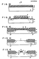
- Si0 2 film 2 is grown by thermal oxidation on a p-type silicon substrate 1 having crystal orientation (100) and Si 3 N 4 film 3 is deposited on this Si0 2 film 2.
- Resist film 4 is formed by photolithography at a portion where an element is to be formed and, using resist film 4 as a mask, Si 3 N 4 film 3 except the portion where the element is to be formed is removed by etching to form Si 3 N 4 pattern 3'. Then, ion-implanting boron, for example, p +- regions 5 are formed at a field region to function as channel stopper regions (Fig. 1B).
- Si 3 N 4 pattern 3 1 is a mask to selectively grow thick field oxide film 6 (Fig. 1C).
- Si 3 N 4 pattern 3 1 and Si0 2 film 2 are removed by etching to form a region 7 where the element is to be formed and which is isolated by field oxide film 6 (Fig. l D ).
- gate oxide film 8 on a portion of region 7 is formed.
- Arsenic for example, is diffused into the region 7 except the gate region to form n + -regions 10 and 11 which function as source and drain regions, respectively.
- contact holes 13 are formed at those portions corresponding to n + -regions 10, 11 and gate electrode, and At interconnection layer patterns 14 are further formed, thus finishing an n-channel MOS LSI.
- F ig. 1G is a detailed view showing a cross-sectioned semiconductor in the process shown in Fig. 1C in which field oxide film 6 is formed using Si 3 N 4 pattern 3' as a mask. It is usually well known in the selective oxidation method that field oxide film 6 grows penetrating into a region F under Si 3 N 4 pattern 3 1 .
- This region F comprises a region D, so-called birds' beak formed in such a form that oxidizing agent diffuses into thin Si0 2 film 2 under Si 3 N 4 pattern 3', and a region E formed in such a form that thick oxide film 6 penetrates sideways.
- the length of region F amounts to about 1 ⁇ m in the case where field oxide film 6 having a film thickness of 1 ⁇ m is grown together with 0 S i 3N4 pattern 3 1 having a thickness of 100 nm (1,000 A) and 0 Si0 2 film 2 having a thickness of 100 ⁇ m (1,000 A), for example.
- the width C of field region can not be shortened shorter than 4 ⁇ m because the length of region F is 1 ⁇ m. Therefore, the region F formed by the penetration of field oxide film 6 becomes a big obstacle to high integration of L SI .
- boron ion-implanted as a channel stopper re-diffuses sideways during field oxidation and p +- regions 5 are formed at a portion of region 7 where the element is to be formed, as shown in Fig. 1H, to thereby reduce the width of effective element region from G to H.
- narrow channel effects of reducing the current of transistor and increasing threshold voltage are caused. It is also important to prevent this phenomenon as well as to make elements fine. As shown in Fig.
- the object of the present invention is to provide a method for manufacturing a highly integrated, high reliable and high quality semiconductor device by allowing optional and fine field regions to be formed in self-alignment.
- a method for manufacturing a semiconductor device Comprising steps (a) to (f) of claim 1.
- a semiconductor device manufacturing method comprising steps (a) to (d) of claim 7.
- the present invention is based on a fact that when on the surface of a semiconductor substrate having grooves more than one formed at predetermined portions thereof is deposited insulating material with a thickness larger than half the width of groove opening, grooves are filled with insulating material and when the deposited insulating material layer is then etched, the deposited insulating material layer is still left in grooves even if the insulating material layer is removed at those portions which exclude groove portions.
- the present invention intends to employ this fact in the formation of field region. According to the present invention, optional and fine field regions are formed in self-alignment.
- the present invention makes it possible to overcome various disadvantages caused in the case where conventional selective oxidation as described above is employed.
- grooves are filled regardless of depth of grooves by depositing insulating material with a thickness larger than half the width of groove opening is that the deposition of insulating material has no direction and develops at side faces of grooves.
- etching technique may be employed ion etching, reactive ion etching, wet etching such as KOH and the like. It is not necessarily needed that side faces of a groove is formed vertical. Grooves may be tapered or reversely tapered to have a sloped angle e. When reactive ion etching is used, grooves having substantially vertical side faces are obtained and when silicon substrate having crystal orientation (100) is selectively etched by KOH, grooves tapered to have the sloped angle e are obtained. Tapered grooves may include those having a V-shaped cross section, a flat bottom or curved side faces. The number of grooves may be one or more than two, and grooves may be different from one another in their width and depth.
- insulating material is deposited with a thickness larger than half the groove opening on the whole surface of semiconductor substrate including the inside of grooves to fill grooves with insulating material completely.
- the thickness of insulating material to be deposited may be (a.cot ⁇ /2)/2 wherein "a" represents the width of groove opening.
- insulating material may be used, for,example, Si02, Si3N4, A1 2 0 3 or the like, or low-melting-point insulating material such as phosphorus silicate glass and boron phosphorus silicate glass, if necessary.
- insulating material As the deposition method of insulating material may be employed CVD method and PVD method such as sputtering, or the like.
- CVD method and PVD method such as sputtering, or the like.
- the thickness of insulating material to be deposited is smaller than half the width of groove opening or (a ⁇ cot ⁇ /2)/2, grooves are not completely filled with insulating material to form recesses communicated with groove openings, thus causing such disadvantage that insulating material which is left in grooves and which must not be etched is etched upon the subsequent etching of insulating material on the substrate.
- the inside, preferably only the bottom of grooves may be doped by impurity of same conductivity type as that of substrate to form channel stopper regions in the substrate.
- the whole surface of substrate including the inside surface of grooves or at least a portion of inside surface of grooves may also be subjected to oxidization or nitrization to form oxide film or nitride film not filling grooves. - When this oxide film or nitride film is formed, field regions consist of dense oxide or nitride film and insulating material layer to thereby more extremely enhance element separation capacity as compared with those consisting of insulating material only.
- the whole surface or a part of surface of this insulating material is doped by, for example, boron, phosphorus, arsenic or the like and then heat-treated to melt the doped layer, or low melting insulating material such as boron phosphorus silicate glass (BPSG), phosphorus silicate glass (PSG) and arsenic silicate glass (AsSG) may be deposited on the whole or a part of insulating material layer and then melted.
- BPSG boron phosphorus silicate glass
- PSG phosphorus silicate glass
- AsSG arsenic silicate glass
- the insulating material layer deposited in grooves is recessed depending upon the condition under which insulating material is deposited, one of these treatments enables the recessed portion to be made flat, thus preventing the surface of insulating material in grooves from being made lower than the level of groove opening in the subsequent etching process.
- insulating material film deposited on the semiconductor substrate is removed by etching, without using masking material, until the semiconductor substrate excluding grooves is exposed while leaving insulating material in grooves to thereby form field regions.
- etching may be employed plasma etching, reactive ion etching or the like.
- active elements such as MOS transistor and bipolar transistor are formed at portions where elements are to be formed and which are isolated by field regions thus formed to thereby finish the manufacture of a semiconductor device.
- the method of the present invention enables insulating material to be left in grooves in self-alignment without mask alignment margin to form field regions, thus allowing a semiconductor device having the following various effects to be provided.
- insulating material on the semiconductor substrate excluding grooves is all removed by etching, but the present invention is not limited to this and it is possible to leave a part of insulating material on the semiconductor substrate. Namely, after insulating material is deposited with a thickness larger than half the width of groove opening on the whole surface of semiconductor substrate including grooves to fill grooves with insulating material completely, those regions of insulating material layer on the substrate excluding grooves at which field regions are to be formed and/or partial regions of insulating material layer on the substrate including a part of regions of insulating material layer on grooves are coated with masking material such as resist pattern, for example.
- the insulating material layer is etched leaving the insulating material layer in grooves and at portions coated with the masking layer to thereby form field regions.
- field regions formed on the substrate excluding grooves may be made integral with those formed in grooves.
- Active elements such as MOS transistor and bipolar transistor are then formed at those regions where elements are to be formed and which are isolated by field regions, thus finishing the manufacture of a semiconductor device provided with field regions embedded in grooves and those formed integral with or separated from field regions in grooves on the semiconductor substrate excluding grooves.
- the above-mentioned method has various merits as described above. However, it is certain that the method is advantageous in the formation of LSI having narrow field regions but has a problem in the formation of LSI having wide field regions.
- the width S of field region is determined by that of groove and insulating film must have a thickness (T) which is larger than 1/2S to be left in grooves. Therefore, when the width of field region is large, insulating film must be deposited with a substantially large thickness.
- T thickness
- the thickness of insulating film must be made more than 10 um, which causes many difficult problems as to the depositing time, accuracy of film thickness and condition under which no crack is caused.
- This method enables wide field oxide film to be formed and most disadvantages of selective oxidation method to be overcome, but causes a big disadvantage to occur under certain circumstances. Namely, flatness is lost because of stepped portion caused at the end of wide field film.
- the half of field film is embedded in the silicon substrate, but in the case of this method, the whole thickness of field film distributes to the formation of stepped portion so that the stepped portion is made extremer as compared with that in the selective oxidation method, which becomes a big obstacle in the case where micro-lithography is needed at the regions adjacent to the wide field film.
- the other comprises forming in the semiconductor substrate by same method as the above-mentioned one first grooves which are at least two and which are adjacent to one another, filling these first grooves with insulating material, removing by etching that portion of semiconductor substrate which is between any two of insulating material layers filled in first adjacent grooves to.form a second groove or grooves, subjecting the second groove(s) to field oxidation using oxidation-resistive film as a mask to fill the second groove(s) with oxide film and making coalescent the oxide film with insulating material filled l in first grooves positioned on both sides of second groove(s) to result in a wide field region.
- the MOS LSI manufactured in this Example had narrow field region 66a and wide field region 73, and the silicon substrate 21 was made flat with no stepped portion formed between field regions and element forming region after the formation of field regions 66a and 73, as shown in Fig. 21. Therefore, when At electrodes 80 and 81 were formed, such stepped portion as seen at the end of field region 54c in Example 5 was not caused and disconnection of metal electrode between field regions and element forming region could be prevented.
- p + -regions 64 and 71 which function as channel stopper regions, were arranged under the bottom of grooves 63a, 63b - 63e and 68a - 68c and therefore not diffused into the element forming region, thus preventing the element property from being degrade due to narrow channel effect and the floating capacity of n +- regions 76 and 77 from being increased due to the contact between p + -regions 64, 71 and n +- regions 76, 77, which function as source and drain. Further, the occurrence of leak current between elements could be prevented. Accordingly, a high quality and highly integrated MOS LSI could be obtained.
- Example 2 As described above, various disadvantages caused when the selective oxidation method was employed could be eliminated and a field insulating region having an optional width and no stepped portion could also be formed. Therefore, Example 2 could greatly contribute the manufacture of highly integrated and high quality LSI.
- Example 2 the field oxide film 92 is formed integral with both field insulating films 86b and 86c. Instead, it may be separated from one or both of the films 86b and 86c.
Landscapes
- Element Separation (AREA)
Abstract
- (a) forming a plurality of first grooves (63a-63e);
- (b) depositing an insulating material (65) on the whole surface of the semiconductor substrate (21) to fill the first grooves (63a-63e);
- (c) etching the insulating material layer (65) to leave the insulating material layer (66a-66e) in the first grooves (63a-63e);
- (d) etching those portions of the semiconductor substrate (21) which are between the insulating material layers (66b-66e) to form second grooves 68a-68c);
- (e) depositing an insulating material (70) on the whole surface of the semiconductor substrate (21) to fill the second groove(s) (68a-68c); and
- (f) etching the insulating material layer (70) to form a field region (73).

Description
- The present invention relates to a method for manufacturing a semiconductor device and, more particularly, to an improvement of element isolation technique for use in the manufacture of semiconductor device.
- Selective oxidation has been conventionally employed as the isolation process in the manufacture of semiconductor device, particularly MOS LSI. An example in which this selective oxidation is applied to the manufacture of n-channel MOS LSI will be set forth below.
- As shown in Fig. lA, Si02 film 2 is grown by thermal oxidation on a p-
type silicon substrate 1 having crystal orientation (100) and Si3N4 film 3 is deposited on this Si02 film 2. Resist film 4 is formed by photolithography at a portion where an element is to be formed and, using resist film 4 as a mask, Si3N4film 3 except the portion where the element is to be formed is removed by etching to form Si3N4 pattern 3'. Then, ion-implanting boron, for example, p+-regions 5 are formed at a field region to function as channel stopper regions (Fig. 1B). After resist film 4 is removed, wet oxidation is applied using Si3N4 pattern 31 as a mask to selectively grow thick field oxide film 6 (Fig. 1C). Si3N4 pattern 31 and Si02 film 2 are removed by etching to form aregion 7 where the element is to be formed and which is isolated by field oxide film 6 (Fig. lD). As shown in Fig. lE, on a portion ofregion 7 is formedgate oxide film 8, on which gate electrode 9 is further formed. Arsenic, for example, is diffused into theregion 7 except the gate region to form n+-regions contact holes 13 are formed at those portions corresponding to n+-regions interconnection layer patterns 14 are further formed, thus finishing an n-channel MOS LSI. - This method as described above and employing selective oxidation to manufacture MOS LSI has the following various disadvantages:
- Fig. 1G is a detailed view showing a cross-sectioned semiconductor in the process shown in Fig. 1C in which
field oxide film 6 is formed using Si3N4 pattern 3' as a mask. It is usually well known in the selective oxidation method thatfield oxide film 6 grows penetrating into a region F under Si3N4 pattern 31. This region F comprises a region D, so-called birds' beak formed in such a form that oxidizing agent diffuses into thin Si02 film 2 under Si3N4 pattern 3', and a region E formed in such a form thatthick oxide film 6 penetrates sideways. The length of region F amounts to about 1 µm in the case wherefield oxide film 6 having a film thickness of 1 µm is grown together with 0 Si3N4 pattern 31 having a thickness of 100 nm (1,000 A) and 0 Si02 film 2 having a thickness of 100 µm (1,000 A), for example. - For this reason, providing that the distance A between two Si3N4 patterns 31 is 2 µm, the width C of field region can not be shortened shorter than 4 µm because the length of region F is 1 µm. Therefore, the region F formed by the penetration of
field oxide film 6 becomes a big obstacle to high integration of LSI. - This leads to the employment of methods of suppressing the formation of birds' beak region D by thickening Si3N4 pattern 3' and thinning Si02 film 2 under Si3N4 pattern 31 and of suppressing the formation of region F by growing
field oxide 6 thin. However, according to the former method, stress becomes large at the end portion of field region to easily cause failure and according to the latter method, a problem is caused that field inversion voltage is reduced. Therefore, the selective oxidation method has a limit in the attempt of highly integrating elements. - In addition, according to the selective oxidation method, boron ion-implanted as a channel stopper re-diffuses sideways during field oxidation and p+-regions 5 are formed at a portion of
region 7 where the element is to be formed, as shown in Fig. 1H, to thereby reduce the width of effective element region from G to H. As a result, narrow channel effects of reducing the current of transistor and increasing threshold voltage are caused. It is also important to prevent this phenomenon as well as to make elements fine. As shown in Fig. 1I, the area at which n+-region 11 (or 10) is contacted with p+-region 5 in theelement forming region 7 becomes larger by p+-region 5 enlarged sideways to thereby make larger a floating capacitor between n+-regions substrate 1. This floating capacitor can not be neglected as elements become smaller. - The object of the present invention is to provide a method for manufacturing a highly integrated, high reliable and high quality semiconductor device by allowing optional and fine field regions to be formed in self-alignment.
- According to the present invention is provided a method for manufacturing a semiconductor device Comprising steps (a) to (f) of
claim 1. - According to the present invention is further provided a semiconductor device manufacturing method comprising steps (a) to (d) of
claim 7. - This invention can be more fully understood from the following detailed description when taken in conjunction with the accompanying drawings, in which:
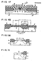
- Figs. 1A -1I are sectional views showing the conventional n-channel MOS LSI manufacturing process in which selective oxidation is employed;
- Figs. 2A-2J are sectional views showing a process of manufacturing an n-channel MOS LSI in example 1 of the present invention;
- Figs. 3A-3K are sectional views showing process of manufacturing an n-channel MOS LSI in example 2;
- Fig. 4 is a sectional view showing a variation of example 2; and'
- Figs. 5A-5C are sectional views showing other variations of example 2.
- The present invention is based on a fact that when on the surface of a semiconductor substrate having grooves more than one formed at predetermined portions thereof is deposited insulating material with a thickness larger than half the width of groove opening, grooves are filled with insulating material and when the deposited insulating material layer is then etched, the deposited insulating material layer is still left in grooves even if the insulating material layer is removed at those portions which exclude groove portions. The present invention intends to employ this fact in the formation of field region. According to the present invention, optional and fine field regions are formed in self-alignment.
- Therefore, the present invention makes it possible to overcome various disadvantages caused in the case where conventional selective oxidation as described above is employed.
- The reason why grooves are filled regardless of depth of grooves by depositing insulating material with a thickness larger than half the width of groove opening is that the deposition of insulating material has no direction and develops at side faces of grooves.
- The present invention will be now described in detail.
- After masking material like resist pattern, for example, is formed on a semiconductor substrate except those portions where grooves are to be formed, the semiconductor substrate exposed through openings of this masking material is etched by a desired depth to form grooves. As etching technique may be employed ion etching, reactive ion etching, wet etching such as KOH and the like. It is not necessarily needed that side faces of a groove is formed vertical. Grooves may be tapered or reversely tapered to have a sloped angle e. When reactive ion etching is used, grooves having substantially vertical side faces are obtained and when silicon substrate having crystal orientation (100) is selectively etched by KOH, grooves tapered to have the sloped angle e are obtained. Tapered grooves may include those having a V-shaped cross section, a flat bottom or curved side faces. The number of grooves may be one or more than two, and grooves may be different from one another in their width and depth.
- After masking material is removed, insulating material is deposited with a thickness larger than half the groove opening on the whole surface of semiconductor substrate including the inside of grooves to fill grooves with insulating material completely. In the case of tapered grooves whose side faces have the sloped angle e, the thickness of insulating material to be deposited may be (a.cotθ/2)/2 wherein "a" represents the width of groove opening. As insulating material may be used, for,example, Si02, Si3N4, A1203 or the like, or low-melting-point insulating material such as phosphorus silicate glass and boron phosphorus silicate glass, if necessary. As the deposition method of insulating material may be employed CVD method and PVD method such as sputtering, or the like. When the thickness of insulating material to be deposited is smaller than half the width of groove opening or (a·cotθ/2)/2, grooves are not completely filled with insulating material to form recesses communicated with groove openings, thus causing such disadvantage that insulating material which is left in grooves and which must not be etched is etched upon the subsequent etching of insulating material on the substrate.
- Prior to the deposition of insulating material, the inside, preferably only the bottom of grooves may be doped by impurity of same conductivity type as that of substrate to form channel stopper regions in the substrate. Prior to the deposition of insulating material, the whole surface of substrate including the inside surface of grooves or at least a portion of inside surface of grooves may also be subjected to oxidization or nitrization to form oxide film or nitride film not filling grooves. - When this oxide film or nitride film is formed, field regions consist of dense oxide or nitride film and insulating material layer to thereby more extremely enhance element separation capacity as compared with those consisting of insulating material only.
- After the deposition of insulating material, the whole surface or a part of surface of this insulating material is doped by, for example, boron, phosphorus, arsenic or the like and then heat-treated to melt the doped layer, or low melting insulating material such as boron phosphorus silicate glass (BPSG), phosphorus silicate glass (PSG) and arsenic silicate glass (AsSG) may be deposited on the whole or a part of insulating material layer and then melted. When the insulating material layer deposited in grooves is recessed depending upon the condition under which insulating material is deposited, one of these treatments enables the recessed portion to be made flat, thus preventing the surface of insulating material in grooves from being made lower than the level of groove opening in the subsequent etching process.
- Then, insulating material film deposited on the semiconductor substrate is removed by etching, without using masking material, until the semiconductor substrate excluding grooves is exposed while leaving insulating material in grooves to thereby form field regions. As etching may be employed plasma etching, reactive ion etching or the like.
- Thereafter, active elements such as MOS transistor and bipolar transistor are formed at portions where elements are to be formed and which are isolated by field regions thus formed to thereby finish the manufacture of a semiconductor device.
- As described above, the method of the present invention enables insulating material to be left in grooves in self-alignment without mask alignment margin to form field regions, thus allowing a semiconductor device having the following various effects to be provided.
-
- (1) The area of field region is determined by the area of inside surface of groove formed in the - substrate. Therefore, fine field region can be easily formed by masking smaller the area of inside surface of groove to thereby provide a highly integrated semiconductor device.
- (2) Regardless of area thereof, the depth of field region is determined by the depth of groove and can be optionally selected by adjusting the depth of groove. Therefore, current leak between elements can be surely prevented at field region by deepening the groove to form a deep field region, thus allowing a high quality semiconductor device to be provided.
- (3) After impurity for channel stopper is implanted to the surfaces of grooves, the thermal oxidation step carried out under high temperature and for a long time in the conventional selective oxidation method is not'employed, thus preventing impurity regions in the inside surface of grooves from being re-diffused to penetrate into the surface of portions where elements are to be formed and to make smaller effective element forming regions. When the doping of impurity is carried out by ion-implantation in this case, the ion-implanted layer can be formed only on the bottom of grooves and even if impurity in the ion-implanted layer is re-diffused, the ion-implanted layer is not penetrated into the surface of element forming regions, thus preventing bad influence from acting on impurity regions formed at element forming regions as well as effective element forming regions from being made smaller.
- (4) When field regions are formed leaving insulating material in grooves in such a form that grooves are completely filled with insulating material, the substrate is made flat, thus preventing interconnection electrodes from being disconnected in the subsequent formation of interconnection electrodes.
- In the embodied mode of the present invention as described above, insulating material on the semiconductor substrate excluding grooves is all removed by etching, but the present invention is not limited to this and it is possible to leave a part of insulating material on the semiconductor substrate. Namely, after insulating material is deposited with a thickness larger than half the width of groove opening on the whole surface of semiconductor substrate including grooves to fill grooves with insulating material completely, those regions of insulating material layer on the substrate excluding grooves at which field regions are to be formed and/or partial regions of insulating material layer on the substrate including a part of regions of insulating material layer on grooves are coated with masking material such as resist pattern, for example. Until portions of substrate excluding portions coated with the masking layer and grooves are exposed, the insulating material layer is etched leaving the insulating material layer in grooves and at portions coated with the masking layer to thereby form field regions. In this case, field regions formed on the substrate excluding grooves may be made integral with those formed in grooves. Active elements such as MOS transistor and bipolar transistor are then formed at those regions where elements are to be formed and which are isolated by field regions, thus finishing the manufacture of a semiconductor device provided with field regions embedded in grooves and those formed integral with or separated from field regions in grooves on the semiconductor substrate excluding grooves.
- The above-mentioned method has various merits as described above. However, it is certain that the method is advantageous in the formation of LSI having narrow field regions but has a problem in the formation of LSI having wide field regions. The width S of field region is determined by that of groove and insulating film must have a thickness (T) which is larger than 1/2S to be left in grooves. Therefore, when the width of field region is large, insulating film must be deposited with a substantially large thickness. When a field region having a width of 20 um is formed, for example, the thickness of insulating film must be made more than 10 um, which causes many difficult problems as to the depositing time, accuracy of film thickness and condition under which no crack is caused. In addition, it becomes extremely difficult to form by the above-mentioned method a field region which has a thickness of 200 pm and which resides under At bonding pad, for example. Therefore, in the case of needing a wide field region, such a method can be employed that a narrow field region is embedded according to the above-mentioned method, insulating film (Si02), for example, is then deposited and removed by photo-etching leaving some part thereof to form a wide field region.
- This method enables wide field oxide film to be formed and most disadvantages of selective oxidation method to be overcome, but causes a big disadvantage to occur under certain circumstances. Namely, flatness is lost because of stepped portion caused at the end of wide field film. In the case of selective oxidation method, the half of field film is embedded in the silicon substrate, but in the case of this method, the whole thickness of field film distributes to the formation of stepped portion so that the stepped portion is made extremer as compared with that in the selective oxidation method, which becomes a big obstacle in the case where micro-lithography is needed at the regions adjacent to the wide field film.
- The following two methods are employed to overcome these disadvantages and to form wide field regions:
- One of them comprises forming in the semiconductor substrate by same method as the above-mentioned one first grooves which are at least two and which are adjacent to one another, filling these first grooves with insulating material, removing by etching that portion of semiconductor substrate which is between any two of insulating material layers filled in first adjacent grooves to form a second groove or:grooves, filling the second groove with insulating material in same manner as to fill first grooves and making coalescent the insulating material layer in the second groove(s) with those in first grooves positioned on both sides of second groove(s) to result in a wide field region.
- The other comprises forming in the semiconductor substrate by same method as the above-mentioned one first grooves which are at least two and which are adjacent to one another, filling these first grooves with insulating material, removing by etching that portion of semiconductor substrate which is between any two of insulating material layers filled in first adjacent grooves to.form a second groove or grooves, subjecting the second groove(s) to field oxidation using oxidation-resistive film as a mask to fill the second groove(s) with oxide film and making coalescent the oxide film with insulating material filled l in first grooves positioned on both sides of second groove(s) to result in a wide field region.
- In these two methods to form wide field regions, it is possible to form one or more other grooves at a position remote from the group of first adjacent grooves.
- Various variations of above-mentioned method to form narrow field regions can also be applied to these two methods.
- Examples in which the method of the present invention is applied to the manufacture of n-channel MOS LSI will be described with reference to the drawings.
-
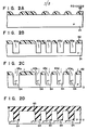
- (I) A resist film was selectively removed, thus providing a resist
pattern 62 which would be used as a mask for cutting grooves in a p-type silicon substrate 21 having crystal face (100) (Fig. 2A). Thesilicon substrate 21 was then etched by reactive ion-etching using the resistpattern 62 as a mask. As shown in Fig. 2B, a plurality offirst grooves 63a - 63e each having vertical side faces were formed. Thegroove 63a had a width of 1.5 um and a depth of 2 µm and separated enough from other grooves.Grooves 63b - 63e each having a width of 1 µm and a depth of 2 µm were formed adjacent to one another with a space of 1 µm interposed therebetween. After boron, which is an impurity of same conductivity type as that ofsubstrate 21, was ion-implanted under accelerating voltage of 50 keV and dose of 5 x 10¹² /cm2 using the resist pattern as the mask, heat treatment was applied thereto to form p+-regions.64 under the bottom ofgrooves 63a - 63e, said p+-regions 64 functioning as channel stopper regions (Fig. 2C). - (II) After the resist
pattern 62 was removed, Si02 was deposited by CVD with a thickness (1.0 um) larger than half (0.75 µm) the opening width ofgroove 63a. Si02 was gradually deposited on thesubstrate 21 and the inner surface ofgrooves 63a - 63e and a CVD-Si02 film 65 was formed completely fillinggrooves 63a - 63e, as shown in Fig. 2D. Because heat treatment carried out under high temperature and for a long time in the selective oxidation method was made unnecessary at the time of SiO2 deposition, no re-diffusion of the impurity in p+-regions 64 occurred. - (III) The whole surface of CVD-Si02 film 65 was etched by ammonium fluoride until the main surface of
silicon substrate 21 was exposed. The CVD-Si02 film 65 on thesubstrate 21 was removed at this time by the amount corresponding to the thickness thereof to leave CVD-Si0 2 66a - 66e infirst grooves 63a - 63e. - (IV) As shown in Fig. 2F, a resist
film 67 is formed on thesubstrate 21 including a part of CVD-Si0 2 66b and a part of CVD-Si0 2 66e, leaving the other CVD-SiO Si0 film 67 as a mask, thesubstrate 21 is subjected to reactive ion-etching. As a result, thesilicon substrate 21 left uncovered and exposed among CVD-SiO 2 66b - 66e was selectively removed at this time to form second threegrooves substrate 21, was then ion-implanted under accelerating voltage of 50 keV and dose of 5x 10 12 /cm2 using the resistfilm 67 as the mask, heat treatment was applied thereto to form p+-regions 69, which function as channel stopper regions, under the bottom ofsecond grooves 68a - 68c (Fig. 2G). - (V) After the resist
film 67 was removed, Si02 was deposited by CVD with a thickness (0.8 pm) larger than half (0.5 pm) the opening width ofgrooves 68a - 68c. Si02 was gradually deposited on thesubstrate 21 and the inner surface ofsecond grooves 68a - 68c and a CVD-Si02 film 70 was formed completely fillingsecond grooves 68a - 68c, as shown in Fig. 2H. During the CVD process, p+-regions 64 formed under the bottom offirst grooves 63b - 63e were made integral with p+-regions 69 formed under the bottom ofsecond grooves 68a - 68c to form a wide p+-region 71. - (VI) The whole surface of CVD-Si02 film 70 was etched by ammonium fluoride until the main surface of
silicon substrate 21 was exposed. As shown in Fig. 2I, the CVD-Si02 film on the substrate .21 was removed by the amount corresponding to the thickness thereof, and CVD-Si02 72a - 72c left insecond grooves 68a - 68c were made integral with CVD-Si0 2 66b - 66e to form afield region 73 having a width of 7 µm. CVD-SiO2 left in thefirst groove 63a could be used as a field region having a width of 1.5 pm. Thereafter, a gate electrode 75 consisting of polycrystalline silicon was formed with agate oxide film 74 interposed therebetween on an island region which was isolated by thenarrow field region 66a and thewide field region 73 and where elements-were to be formed, and arsenic diffusion was applied thereto to form n+-regions film 78 consisting of CVD-Si02 was further deposited and after contact holes 79 (the contact hole for gate electrode was not shown) were formed at those portions of interposing insulatingfilm 78 which corresponded to gate electrode 75 and n+-regions 76, 77, an At film was vacuum-vapored to the whole surface thereof and was patterned to form an Atelectrode 80 for source, an Atelectrode 81 for drain, and an At electrode for gate (not shown), thus finishing the manufacture of an n-channel MOS LSI (Fig. 2J). - The MOS LSI manufactured in this Example had
narrow field region 66a andwide field region 73, and thesilicon substrate 21 was made flat with no stepped portion formed between field regions and element forming region after the formation offield regions electrodes regions grooves regions -
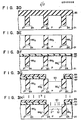
- (I) A resist
film 82 was patterned by photolithography on the p-type silicon substrate 21 having crystal orientation (100) (Fig. 3A). - (II) Etching was applied thereto using the resist
film 82 as a mask to formnarrow grooves 83 each having vertical or substantially vertical side faces. Each ofgrooves 83 had a depth of 2 um, for example. As etching method may be employed ion etching or reactive ion-etching (Fig. 3B). - (III) Boron, for example, was ion-implanted under accelerating voltage of 50 keV and dose of 5 x 10¹² /cm2 using the resist
film 82 as the mask, to thereby form p+-regions (or channel stopper regions) under the bottom of grooves 83 (Fig. 3C). - (IV) After the resist
film 82 was removed, an insulating film 85 (CVD-Si02 film or Si3N4 film, for example) was deposited with a thickness larger than half the width of groove opening (when the width of groove is 0.1 µm, for example, the film thickness becomes 0.6 µm, for example, larger than 0.5 µm) to fill grooves (Fig. 3D). - (V) The insulating
film 85 was etched until thesilicon substrate 21 was exposed to leavefield insulating films - (VI) A thin insulating film 87 (thermal oxide film of 500 A thickness, for example) was formed on the
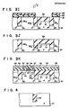
silicon substrate 21 and an oxidation-resistive film 88 (Si3N4 film of 3,000 A, for example) was deposited on the insulating film 87 (Fig. 3F) . - (VII) After the oxidation-
resistive film 88 was coated by a resistfilm 89, the resistfilm 89 was patterned by photolithography removing a region betweenfield insulating films resistive film 88 was etched using the resistfilm 89 as a mask, the thin insulatingfilm 87 and then thesilicon substrate 21 were further etched to form agroove 90. Thesilicon substrate 21 is etched in such way that thefield insulating films film 87 orsilicon substrate 21 is etched, the resistfilm 89 may be removed and etching be then applied thereto using the oxidation-resistive film 88 as the mask. Although the depth by which thesilicon substrate 21 is etched depends upon the condition of subsequent oxidation and the like, the etching depth ofsilicon substrate 21 was made 500 mµ for example, in this Example. - (VIII) Using the resist film 89 (or the oxidation-
resistive film 88 when the resistfilm 89 was removed by the step (VII)) as the mask, boron, for example, was ion-implanted under accelerating voltage of 50 keV and dose of 1 x 10¹³ /cm2 to form a p+-region 91 under the bottom of groove 90 (Fig. 3H) . - (IX) After the resist
film 89 was removed, field oxidation was carried out using the oxidationresistive film 88 as the mask to form between embeddedfield insulating films field oxide film 92 having a film thickness of 1 µm, for example, saidfield oxide film 92 functioning as a wide field insulating film. If thefield oxide film 92 is formed to have a thickness two times the etching depth ofsilicon substrate 21, it can be formed flat in the same level as the element forming region (Fig. 31). When the Si3N4 film or the like is used as embeddedfield insulating films field oxide film 92 penetrated sideways at the time of field oxidation is caused in principle. Or when the Si02 film is used as embeddedfield insulating films - (X) The oxidation-
resistive film 88 and the thin insulatingfilm 87 under the oxidation-resistive film 88 were removed by etching (Fig. 3J). - (XI)
Gate oxide film 93 and gate electrode (polycrystalline silicon, for example) 94 were formed, arsenic, for example, was diffused to form n+-regions 95, an interposing insulating film (CVD-Si02 film, for example) was deposited, contact holes 97 were formed, and Atinterconnection electrode 98, for example, were arranged, thus finishing the main process of manufacturing an LSI (Fig. 3K). - According to Example 2 as described above, various disadvantages caused when the selective oxidation method was employed could be eliminated and a field insulating region having an optional width and no stepped portion could also be formed. Therefore, Example 2 could greatly contribute the manufacture of highly integrated and high quality LSI.
- Variations cf Example 2 will be now described.
- (1) Although ion implantation was carried out to form p+-regions 84 (channel stopper regions) in Example 2 shown in Figs. 3A-3K ion implantation may not be carried out because p+-
regions 84 are not necessarily needed depending upon the condition of impurity concentration contained in thesilicon substrate 21. The mask employed at the time of ion implantation is not limited to the resistfilm 82 but may be the insulating film. - (2) Before
grooves 83 are filled with the insulatingfilm 85, an insulatingfilm 99 may be grown inside grooves 83 (Fig. 4). This insulatingfilm 99 may be formed by oxidizing thesilicon substrate 21, for example, or the CVD film or the like may be deposited. The opening width ofgrooves 83 is made narrower by two times the film thickness of insulatingfilm 99. - (3) When the insulating
film 85 is etched leavingfield insulating films grooves 83, the upper surface offield insulating films silicon substrate 21 to form recesses. - (4)
Field insulating films - (5) The insulating
film 85 is deposited fillinggrooves 83 completely and a low-melting-point insulating film (such as boron phosphorus silicate glass (BPSG), phosphorus silicate glass (PSG) and arsenic silicate glass (AsSG), for example) is then deposited thereon. After the low-melting-point insulating film is then melted, the insulatingfilm 85 may be etched leaving the insulatingfilm 85 embedded ingrooves 83. - (6) The above-mentioned low-melting-point insulating film may be used instead of insulating
film 85. Or two layer construction may be employed using a melting film and a non-melting film. - (7) Although the Si3N4 film was used as the oxidation-
resistive film 88 in Example 2 shown in Figs. 5A-5K, whatever film such as an A1203 film and the thick Si02 film, for example, and capable of suppressing the oxidation ofsilicon substrate 21 may be employed. - (8) Although oxidation-
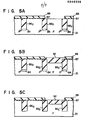
resistive film 88 andsilicon substrate 21 were etched by photolithography after the oxidation-resistive film 88 was deposited in Example 2 shown in Figs. 3A - 3K thesilicon substrate 21 may be etched at first to form thegroove 90, the oxidation-resistive film 88 be deposited, the oxidation-resistive film 88 left in thegroove 90 be etched by photolithography, and field oxidation then be applied thereto. - (9) Although the
silicon substrate 21 was etched to form thegroove 90 after the oxidation-resistive film 88 was etched, and field oxidation was then =applied thereto, field oxidation may be carried out without etching thesilicon substrate 21 after the oxidation-resistive film 88 is etched (Figs. 5A and 5B). The flatness between the field region and the element forming region is lost more or less in this case, but the effect of suppressing the diffusion of channel stopper regions or p+-regions into the element forming region is made great. It is not necessarily needed that the insulatingfilm 87 is deposited at this time. Even if the insulatingfilm 87 is left like the Si02 film on the substrate, the substrate under the insulatingfilm 87 may be oxidized at the time of field oxidation. Therefore, different from Fig. 5A field oxidation may be carried out without etching the thin - insulatingfilm 87. - (10) As a further variation of (9), the
field oxide film 92 may be etched using the oxidation-resistive film 88 to make the structure flat (Fig. 5C). - (11) The variation (10) can be applied to not only those formed by carrying out field oxidation without etching the
silicon substrate 21 as in the variation (9), but also those formed by carrying out field oxidation with thesilicon substrate 21. This is advantageous in the case where, in spite ofsilicon substrate 21 etched, thefield oxide film 92 is formed so thick as to project above the upper surface ofsilicon substrate 21 and to lose the flatness. - In Example 2 the
field oxide film 92 is formed integral with bothfield insulating films films - Although various Examples in which the present invention is applied to the manufacture of n-channel MOS LSI have been described above, it should be understood that the present invention can be applied to the manufacture of a p-channel MOS LSI.
Claims (15)
Applications Claiming Priority (6)
| Application Number | Priority Date | Filing Date | Title |
|---|---|---|---|
| JP9722380A JPS5723239A (en) | 1980-07-16 | 1980-07-16 | Manufacture of semiconductor device |
| JP9722480A JPS5723240A (en) | 1980-07-16 | 1980-07-16 | Manufacture of semiconductor device |
| JP97224/80 | 1980-07-16 | ||
| JP97223/80 | 1980-07-16 | ||
| JP168582/80 | 1980-11-29 | ||
| JP55168582A JPS5791535A (en) | 1980-11-29 | 1980-11-29 | Manufacture of semiconductor device |
Related Parent Applications (1)
| Application Number | Title | Priority Date | Filing Date |
|---|---|---|---|
| EP81105523.5 Division | 1981-07-14 |
Publications (3)
| Publication Number | Publication Date |
|---|---|
| EP0245538A2 true EP0245538A2 (en) | 1987-11-19 |
| EP0245538A3 EP0245538A3 (en) | 1988-02-17 |
| EP0245538B1 EP0245538B1 (en) | 1991-07-10 |
Family
ID=27308349
Family Applications (2)
| Application Number | Title | Priority Date | Filing Date |
|---|---|---|---|
| EP81105523A Expired EP0044082B1 (en) | 1980-07-16 | 1981-07-14 | Method of manufacturing a semiconductor device comprising a dielectric insulating region |
| EP86116670A Expired EP0245538B1 (en) | 1980-07-16 | 1981-07-14 | Method for manufacturing a semiconductor device comprising dielectric isolation regions |
Family Applications Before (1)
| Application Number | Title | Priority Date | Filing Date |
|---|---|---|---|
| EP81105523A Expired EP0044082B1 (en) | 1980-07-16 | 1981-07-14 | Method of manufacturing a semiconductor device comprising a dielectric insulating region |
Country Status (3)
| Country | Link |
|---|---|
| US (1) | US4394196A (en) |
| EP (2) | EP0044082B1 (en) |
| DE (2) | DE3177018D1 (en) |
Cited By (4)
| Publication number | Priority date | Publication date | Assignee | Title |
|---|---|---|---|---|
| EP0513639A3 (en) * | 1991-05-16 | 1992-12-23 | International Business Machines Corporation | Semiconductor field effect transistor device and fabrication thereof |
| US5374583A (en) * | 1994-05-24 | 1994-12-20 | United Microelectronic Corporation | Technology for local oxidation of silicon |
| US5395790A (en) * | 1994-05-11 | 1995-03-07 | United Microelectronics Corp. | Stress-free isolation layer |
| EP0739032A3 (en) * | 1995-04-21 | 1997-10-29 | Samsung Electronics Co Ltd | Method of isolating a semiconductor device |
Families Citing this family (26)
| Publication number | Priority date | Publication date | Assignee | Title |
|---|---|---|---|---|
| EP0073025B1 (en) * | 1981-08-21 | 1989-08-09 | Kabushiki Kaisha Toshiba | Method of manufacturing dielectric isolation regions for a semiconductor device |
| US4563227A (en) * | 1981-12-08 | 1986-01-07 | Matsushita Electric Industrial Co., Ltd. | Method for manufacturing a semiconductor device |
| JPS58132946A (en) * | 1982-02-03 | 1983-08-08 | Toshiba Corp | Manufacture of semiconductor device |
| JPS58165341A (en) * | 1982-03-26 | 1983-09-30 | Toshiba Corp | Manufacture of semiconductor device |
| JPS58171832A (en) * | 1982-03-31 | 1983-10-08 | Toshiba Corp | Preparation of semiconductor device |
| JPS58210634A (en) * | 1982-05-31 | 1983-12-07 | Toshiba Corp | Preparation of semiconductor device |
| FR2529714A1 (en) * | 1982-07-01 | 1984-01-06 | Commissariat Energie Atomique | METHOD FOR PRODUCING THE FIELD OXIDE OF AN INTEGRATED CIRCUIT |
| US4444605A (en) * | 1982-08-27 | 1984-04-24 | Texas Instruments Incorporated | Planar field oxide for semiconductor devices |
| JPS5943545A (en) * | 1982-09-06 | 1984-03-10 | Hitachi Ltd | Semiconductor ic device and its manufacture |
| JPS6088468A (en) * | 1983-10-13 | 1985-05-18 | インタ−ナショナル ビジネス マシ−ンズ コ−ポレ−ション | Method of producing semiconductor integrated circuit |
| US4609413A (en) * | 1983-11-18 | 1986-09-02 | Motorola, Inc. | Method for manufacturing and epitaxially isolated semiconductor utilizing etch and refill technique |
| US4456501A (en) * | 1983-12-22 | 1984-06-26 | Advanced Micro Devices, Inc. | Process for dislocation-free slot isolations in device fabrication |
| JPS6269520A (en) * | 1985-09-21 | 1987-03-30 | Semiconductor Energy Lab Co Ltd | Recess filling method by photo-cvd |
| US5462767A (en) * | 1985-09-21 | 1995-10-31 | Semiconductor Energy Laboratory Co., Ltd. | CVD of conformal coatings over a depression using alkylmetal precursors |
| US4729006A (en) * | 1986-03-17 | 1988-03-01 | International Business Machines Corporation | Sidewall spacers for CMOS circuit stress relief/isolation and method for making |
| FR2598557B1 (en) * | 1986-05-09 | 1990-03-30 | Seiko Epson Corp | METHOD FOR MANUFACTURING A MEMBER ISOLATION REGION OF A SEMICONDUCTOR DEVICE |
| US4980311A (en) * | 1987-05-05 | 1990-12-25 | Seiko Epson Corporation | Method of fabricating a semiconductor device |
| JPH0290617A (en) * | 1988-09-28 | 1990-03-30 | Nec Corp | Manufacture of semiconductor device |
| US5577309A (en) * | 1995-03-01 | 1996-11-26 | Texas Instruments Incorporated | Method for forming electrical contact to the optical coating of an infrared detector |
| US5725739A (en) * | 1996-07-08 | 1998-03-10 | Micron Technology, Inc. | Low angle, low energy physical vapor deposition of alloys |
| JP3417767B2 (en) * | 1996-08-29 | 2003-06-16 | 株式会社東芝 | Manufacturing method of single crystal parts |
| US6333274B2 (en) | 1998-03-31 | 2001-12-25 | Kabushiki Kaisha Toshiba | Method of manufacturing a semiconductor device including a seamless shallow trench isolation step |
| US6265282B1 (en) * | 1998-08-17 | 2001-07-24 | Micron Technology, Inc. | Process for making an isolation structure |
| JP2005008909A (en) * | 2003-06-16 | 2005-01-13 | Canon Inc | Manufacturing method of structure |
| KR101575818B1 (en) * | 2009-08-18 | 2015-12-08 | 삼성전자주식회사 | Method of forming active area structure |
| US8633077B2 (en) | 2012-02-15 | 2014-01-21 | International Business Machines Corporation | Transistors with uniaxial stress channels |
Family Cites Families (14)
| Publication number | Priority date | Publication date | Assignee | Title |
|---|---|---|---|---|
| GB1461943A (en) * | 1973-02-21 | 1977-01-19 | Raytheon Co | Semi-conductor devices |
| US4032373A (en) * | 1975-10-01 | 1977-06-28 | Ncr Corporation | Method of manufacturing dielectrically isolated semiconductive device |
| US4104086A (en) * | 1977-08-15 | 1978-08-01 | International Business Machines Corporation | Method for forming isolated regions of silicon utilizing reactive ion etching |
| US4139442A (en) * | 1977-09-13 | 1979-02-13 | International Business Machines Corporation | Reactive ion etching method for producing deep dielectric isolation in silicon |
| US4140558A (en) * | 1978-03-02 | 1979-02-20 | Bell Telephone Laboratories, Incorporated | Isolation of integrated circuits utilizing selective etching and diffusion |
| US4264382A (en) * | 1978-05-25 | 1981-04-28 | International Business Machines Corporation | Method for making a lateral PNP or NPN with a high gain utilizing reactive ion etching of buried high conductivity regions |
| US4209349A (en) * | 1978-11-03 | 1980-06-24 | International Business Machines Corporation | Method for forming a narrow dimensioned mask opening on a silicon body utilizing reactive ion etching |
| US4209350A (en) * | 1978-11-03 | 1980-06-24 | International Business Machines Corporation | Method for forming diffusions having narrow dimensions utilizing reactive ion etching |
| US4255207A (en) * | 1979-04-09 | 1981-03-10 | Harris Corporation | Fabrication of isolated regions for use in self-aligning device process utilizing selective oxidation |
| US4211582A (en) * | 1979-06-28 | 1980-07-08 | International Business Machines Corporation | Process for making large area isolation trenches utilizing a two-step selective etching technique |
| US4252582A (en) * | 1980-01-25 | 1981-02-24 | International Business Machines Corporation | Self aligned method for making bipolar transistor having minimum base to emitter contact spacing |
| US4318751A (en) * | 1980-03-13 | 1982-03-09 | International Business Machines Corporation | Self-aligned process for providing an improved high performance bipolar transistor |
| US4274909A (en) * | 1980-03-17 | 1981-06-23 | International Business Machines Corporation | Method for forming ultra fine deep dielectric isolation |
| US4307180A (en) * | 1980-08-22 | 1981-12-22 | International Business Machines Corp. | Process of forming recessed dielectric regions in a monocrystalline silicon substrate |
-
1981
- 1981-07-13 US US06/282,642 patent/US4394196A/en not_active Expired - Lifetime
- 1981-07-14 EP EP81105523A patent/EP0044082B1/en not_active Expired
- 1981-07-14 DE DE8181105523T patent/DE3177018D1/en not_active Expired
- 1981-07-14 DE DE8686116670T patent/DE3177250D1/en not_active Expired - Lifetime
- 1981-07-14 EP EP86116670A patent/EP0245538B1/en not_active Expired
Cited By (4)
| Publication number | Priority date | Publication date | Assignee | Title |
|---|---|---|---|---|
| EP0513639A3 (en) * | 1991-05-16 | 1992-12-23 | International Business Machines Corporation | Semiconductor field effect transistor device and fabrication thereof |
| US5395790A (en) * | 1994-05-11 | 1995-03-07 | United Microelectronics Corp. | Stress-free isolation layer |
| US5374583A (en) * | 1994-05-24 | 1994-12-20 | United Microelectronic Corporation | Technology for local oxidation of silicon |
| EP0739032A3 (en) * | 1995-04-21 | 1997-10-29 | Samsung Electronics Co Ltd | Method of isolating a semiconductor device |
Also Published As
| Publication number | Publication date |
|---|---|
| EP0044082A2 (en) | 1982-01-20 |
| EP0044082B1 (en) | 1989-03-22 |
| EP0245538A3 (en) | 1988-02-17 |
| DE3177250D1 (en) | 1991-08-14 |
| EP0245538B1 (en) | 1991-07-10 |
| EP0044082A3 (en) | 1984-09-26 |
| DE3177018D1 (en) | 1989-04-27 |
| US4394196A (en) | 1983-07-19 |
Similar Documents
| Publication | Publication Date | Title |
|---|---|---|
| EP0245538B1 (en) | Method for manufacturing a semiconductor device comprising dielectric isolation regions | |
| KR100227766B1 (en) | Semiconductor device and the manufacturing method thereof | |
| EP0061855B1 (en) | Method for manufacturing semiconductor device | |
| EP0051488B1 (en) | Method for manufacturing a semiconductor device | |
| US4516316A (en) | Method of making improved twin wells for CMOS devices by controlling spatial separation | |
| US4574467A (en) | N- well CMOS process on a P substrate with double field guard rings and a PMOS buried channel | |
| US4743563A (en) | Process of controlling surface doping | |
| US4871685A (en) | Method of manufacturing bipolar transistor with self-aligned external base and emitter regions | |
| EP0073025B1 (en) | Method of manufacturing dielectric isolation regions for a semiconductor device | |
| JPS6219061B2 (en) | ||
| EP0090520B1 (en) | A method of manufacturing a semiconductor device for forming a deep field region in a semiconductor substrate | |
| US4419813A (en) | Method for fabricating semiconductor device | |
| EP0091984B1 (en) | Integrated circuit devices comprising dielectric isolation regions and methods for making such devices | |
| JPH0513566A (en) | Manufacture of semiconductor device | |
| EP0113517A2 (en) | Method for forming an isolation region | |
| JPS6016456A (en) | Semiconductor device | |
| EP0160965B1 (en) | Method of manufacturing a semiconductor device with a stacked-gate-electrode structure | |
| JPS6355780B2 (en) | ||
| US4885261A (en) | Method for isolating a semiconductor element | |
| US5705440A (en) | Methods of fabricating integrated circuit field effect transistors having reduced-area device isolation regions | |
| JPS6119111B2 (en) | ||
| US6080625A (en) | Method for making dual-polysilicon structures in integrated circuits | |
| JPH0338742B2 (en) | ||
| JPH0363220B2 (en) | ||
| JPH0223028B2 (en) |
Legal Events
| Date | Code | Title | Description |
|---|---|---|---|
| PUAI | Public reference made under article 153(3) epc to a published international application that has entered the european phase |
Free format text: ORIGINAL CODE: 0009012 |
|
| 17P | Request for examination filed |
Effective date: 19861229 |
|
| AC | Divisional application: reference to earlier application |
Ref document number: 44082 Country of ref document: EP |
|
| AK | Designated contracting states |
Kind code of ref document: A2 Designated state(s): DE FR GB NL |
|
| PUAL | Search report despatched |
Free format text: ORIGINAL CODE: 0009013 |
|
| AK | Designated contracting states |
Kind code of ref document: A3 Designated state(s): DE FR GB NL |
|
| 17Q | First examination report despatched |
Effective date: 19891031 |
|
| GRAA | (expected) grant |
Free format text: ORIGINAL CODE: 0009210 |
|
| AC | Divisional application: reference to earlier application |
Ref document number: 44082 Country of ref document: EP |
|
| AK | Designated contracting states |
Kind code of ref document: B1 Designated state(s): DE FR GB NL |
|
| ET | Fr: translation filed | ||
| REF | Corresponds to: |
Ref document number: 3177250 Country of ref document: DE Date of ref document: 19910814 |
|
| PLBE | No opposition filed within time limit |
Free format text: ORIGINAL CODE: 0009261 |
|
| STAA | Information on the status of an ep patent application or granted ep patent |
Free format text: STATUS: NO OPPOSITION FILED WITHIN TIME LIMIT |
|
| 26N | No opposition filed | ||
| REG | Reference to a national code |
Ref country code: GB Ref legal event code: 746 Effective date: 19981015 |
|
| REG | Reference to a national code |
Ref country code: FR Ref legal event code: D6 |
|
| PGFP | Annual fee paid to national office [announced via postgrant information from national office to epo] |
Ref country code: DE Payment date: 20000710 Year of fee payment: 20 |
|
| PGFP | Annual fee paid to national office [announced via postgrant information from national office to epo] |
Ref country code: FR Payment date: 20000711 Year of fee payment: 20 |
|
| PGFP | Annual fee paid to national office [announced via postgrant information from national office to epo] |
Ref country code: GB Payment date: 20000713 Year of fee payment: 20 |
|
| PGFP | Annual fee paid to national office [announced via postgrant information from national office to epo] |
Ref country code: NL Payment date: 20000728 Year of fee payment: 20 |
|
| PG25 | Lapsed in a contracting state [announced via postgrant information from national office to epo] |
Ref country code: GB Free format text: LAPSE BECAUSE OF EXPIRATION OF PROTECTION Effective date: 20010713 |
|
| PG25 | Lapsed in a contracting state [announced via postgrant information from national office to epo] |
Ref country code: NL Free format text: LAPSE BECAUSE OF EXPIRATION OF PROTECTION Effective date: 20010714 |
|
| REG | Reference to a national code |
Ref country code: GB Ref legal event code: PE20 Effective date: 20010713 |
|
| NLV7 | Nl: ceased due to reaching the maximum lifetime of a patent |
Effective date: 20010714 |