EP0244848A1 - Method of planarizing inorganic insulating layers for use as intermediate insulating layers in multilevel interconnections - Google Patents
Method of planarizing inorganic insulating layers for use as intermediate insulating layers in multilevel interconnections Download PDFInfo
- Publication number
- EP0244848A1 EP0244848A1 EP87106561A EP87106561A EP0244848A1 EP 0244848 A1 EP0244848 A1 EP 0244848A1 EP 87106561 A EP87106561 A EP 87106561A EP 87106561 A EP87106561 A EP 87106561A EP 0244848 A1 EP0244848 A1 EP 0244848A1
- Authority
- EP
- European Patent Office
- Prior art keywords
- layer
- etching
- organic auxiliary
- inorganic insulation
- auxiliary layer
- Prior art date
- Legal status (The legal status is an assumption and is not a legal conclusion. Google has not performed a legal analysis and makes no representation as to the accuracy of the status listed.)
- Withdrawn
Links
Images

Classifications
-
- H—ELECTRICITY
- H01—ELECTRIC ELEMENTS
- H01L—SEMICONDUCTOR DEVICES NOT COVERED BY CLASS H10
- H01L21/00—Processes or apparatus adapted for the manufacture or treatment of semiconductor or solid state devices or of parts thereof
- H01L21/70—Manufacture or treatment of devices consisting of a plurality of solid state components formed in or on a common substrate or of parts thereof; Manufacture of integrated circuit devices or of parts thereof
- H01L21/71—Manufacture of specific parts of devices defined in group H01L21/70
- H01L21/768—Applying interconnections to be used for carrying current between separate components within a device comprising conductors and dielectrics
- H01L21/76801—Applying interconnections to be used for carrying current between separate components within a device comprising conductors and dielectrics characterised by the formation and the after-treatment of the dielectrics, e.g. smoothing
- H01L21/76819—Smoothing of the dielectric
-
- H—ELECTRICITY
- H01—ELECTRIC ELEMENTS
- H01L—SEMICONDUCTOR DEVICES NOT COVERED BY CLASS H10
- H01L21/00—Processes or apparatus adapted for the manufacture or treatment of semiconductor or solid state devices or of parts thereof
- H01L21/02—Manufacture or treatment of semiconductor devices or of parts thereof
- H01L21/04—Manufacture or treatment of semiconductor devices or of parts thereof the devices having at least one potential-jump barrier or surface barrier, e.g. PN junction, depletion layer or carrier concentration layer
- H01L21/18—Manufacture or treatment of semiconductor devices or of parts thereof the devices having at least one potential-jump barrier or surface barrier, e.g. PN junction, depletion layer or carrier concentration layer the devices having semiconductor bodies comprising elements of Group IV of the Periodic System or AIIIBV compounds with or without impurities, e.g. doping materials
- H01L21/30—Treatment of semiconductor bodies using processes or apparatus not provided for in groups H01L21/20 - H01L21/26
- H01L21/31—Treatment of semiconductor bodies using processes or apparatus not provided for in groups H01L21/20 - H01L21/26 to form insulating layers thereon, e.g. for masking or by using photolithographic techniques; After treatment of these layers; Selection of materials for these layers
- H01L21/3105—After-treatment
- H01L21/31051—Planarisation of the insulating layers
- H01L21/31053—Planarisation of the insulating layers involving a dielectric removal step
- H01L21/31055—Planarisation of the insulating layers involving a dielectric removal step the removal being a chemical etching step, e.g. dry etching
-
- H—ELECTRICITY
- H01—ELECTRIC ELEMENTS
- H01L—SEMICONDUCTOR DEVICES NOT COVERED BY CLASS H10
- H01L21/00—Processes or apparatus adapted for the manufacture or treatment of semiconductor or solid state devices or of parts thereof
- H01L21/02—Manufacture or treatment of semiconductor devices or of parts thereof
- H01L21/04—Manufacture or treatment of semiconductor devices or of parts thereof the devices having at least one potential-jump barrier or surface barrier, e.g. PN junction, depletion layer or carrier concentration layer
- H01L21/18—Manufacture or treatment of semiconductor devices or of parts thereof the devices having at least one potential-jump barrier or surface barrier, e.g. PN junction, depletion layer or carrier concentration layer the devices having semiconductor bodies comprising elements of Group IV of the Periodic System or AIIIBV compounds with or without impurities, e.g. doping materials
- H01L21/30—Treatment of semiconductor bodies using processes or apparatus not provided for in groups H01L21/20 - H01L21/26
- H01L21/31—Treatment of semiconductor bodies using processes or apparatus not provided for in groups H01L21/20 - H01L21/26 to form insulating layers thereon, e.g. for masking or by using photolithographic techniques; After treatment of these layers; Selection of materials for these layers
- H01L21/3105—After-treatment
- H01L21/311—Etching the insulating layers by chemical or physical means
- H01L21/31105—Etching inorganic layers
- H01L21/31111—Etching inorganic layers by chemical means
- H01L21/31116—Etching inorganic layers by chemical means by dry-etching
Definitions
- the invention relates to a method for planarizing the surface of an inorganic insulation layer, such as is used as an intermediate layer for multilayer metallizations of highly integrated semiconductor circuits, in which the planarization process is supported by the participation of an organic auxiliary layer and an etch-back process.
- the object of the invention is therefore to provide a method with which an almost flat surface is achieved after the production of the inorganic insulation layer.
- the method should be applicable for structure distances of less than 2 ⁇ m and structure heights of less than 1 ⁇ m.
- This process control solves the problem in a simple manner, that is, narrow gaps are also filled with the insulation material, since the process is repeated until all the gaps into which the above-mentioned layers can be deposited are filled.
- the use of the organic auxiliary layer and its complete removal by etching in the magnetron etching system ensures that the full gap width is retained and the inorganic insulation layer in the gap floor is not thinned.
- the method according to the teaching of the invention offers the possibility of producing highly integrated semiconductor circuits, in particular CMOS modules, with more than three wiring levels even on uneven substrates and with structure spacings of less than 2 ⁇ m. Electromigration effects and etching residues do not occur; the service life for current-loaded conductor tracks is tripled.
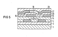
- the reference numeral 15 denotes the second metallization, 16 and 26 the second intermediate oxide layer, 17 the third metallization and 18 and 28 the third intermediate oxide layer or passivation layer.
- FIGS. 1 and 5 clearly shows the advantages of the method according to the invention.
Abstract
Description
Die Erfindung betrifft ein Verfahren zum Planarisieren der Oberfläche einer anorganischen Isolationsschicht, wie sie als Zwischenschicht für Mehrlagenmetallisierungen von hochintegrierten Halbleiterschaltungen verwendet wird, bei dem der Planarisierungsprozeß durch Mitwirkung einer organischen Hilfsschicht und eines Rückätzverfahrens unterstützt wird.The invention relates to a method for planarizing the surface of an inorganic insulation layer, such as is used as an intermediate layer for multilayer metallizations of highly integrated semiconductor circuits, in which the planarization process is supported by the participation of an organic auxiliary layer and an etch-back process.
Die zunehmende Packungsdichte bei hochintegrierten Halbleiterschaltungen bringt, aufgrund der dadurch bedingten Verringerung der lateralen Strukturabmessungen ohne entsprechende Abnahme der Schichtdicke und der Zunahme der Verdrahtungsebenen, Probleme bei der Strukturierung und der Kantenbedeckung der Leiterbahnen mit sich. Zur Behebung dieser Schwierigkeiten ist, besonders bei mehr als drei Verdrahtungsebenen, eine möglichst weitgehende Einebnung der vorangehenden Leiterbahnebene(n) durch die diese isolierende Schicht notwendig.The increasing packing density in highly integrated semiconductor circuits, due to the resulting reduction in the lateral structure dimensions without a corresponding decrease in the layer thickness and the increase in the wiring levels, brings with it problems in the structuring and edge coverage of the conductor tracks. To eliminate these difficulties, especially with more than three wiring levels, a leveling of the preceding conductor level (s) as far as possible by the insulating layer is necessary.
Aufgabe der Erfindung ist es daher, ein Verfahren anzugeben, mit dem eine nahezu ebene Oberfläche nach der Herstellung der anorganischen Isolationsschicht erreicht wird. Insbesondere soll das Verfahren anwendbar sein für Strukturabstände kleiner 2 µm und Strukturhöhen kleiner 1 µm.The object of the invention is therefore to provide a method with which an almost flat surface is achieved after the production of the inorganic insulation layer. In particular, the method should be applicable for structure distances of less than 2 µm and structure heights of less than 1 µm.
Aus dem J. Electrochem. Soc. 128 (1981) ist auf den Seiten 423 bis 429 aus einem Bericht von Adams und Capio ein Verfahren zur Einebnung bzw. Planarisierung einer anorganischen Isolationsschicht bekannt, welches auf dem Ätzen einer mit Photolack weitgehend eingeebneten Isolationsschicht bei gleicher Ätzrate für den Lack und das Isolationsmaterial beruht. Der Photolack wirkt dabei als Hilfsschicht. Der Planarisierungsprozeß wird als Rückätzprozeß bezeichnet. Begrenzt wird dieses Verfahren durch die Abscheidung der anorganischen Isolationsschicht(en), vor allem dann, wenn diese aus der plasmainduzierten Gasphase geschieht. Enge Spalte und Löcher werden nicht gefüllt. Bei entsprechendem Verhältnis von Leitbahnabstand und gewünschter Isolationsschichtdicke entstehen Kavernen, die bei dem Rückätzen geöffnet werden können und dann zu unzulässigen Anätzungen des Untergrundes führen.From J. Electrochem. Soc. 128 (1981) is on pages 423 to 429 from a report by Adams and Capio a method for leveling or planarizing an inorganic insulation layer is known, which is based on the etching of an insulation layer largely leveled with photoresist at the same etching rate for the lacquer and the insulation material. The photoresist acts as an auxiliary layer. The planarization process is called the etch-back process. This process is limited by the deposition of the inorganic insulation layer (s), especially if this occurs from the plasma-induced gas phase. Narrow gaps and holes are not filled. With an appropriate ratio of the spacing of the interconnect and the desired insulation layer thickness, caverns are created that can be opened during the etching back and then lead to inadmissible etching of the substrate.
Ein weiteres Verfahren, bei dem auch eine organische Hilfsschicht und ein Rückätzverfahren verwendet wird, ist aus der DE-OS 33 45 040 A1 bekannt. Bei diesem Verfahren erfolgt die Einebnung mit Hilfe einer Polyimidschicht, die auf die zu isolierende und mit der Metallisierung versehene Oberfläche aufgebracht und dann durch ein Trockenätzverfahren ganzflächig soweit wieder entfernt wird, bis die Metallisierung freigelegt ist. Erst dann wird darauf die anorganische Isolationsschicht bis zur gewünschten Isolatordicke abgeschieden. Dieses Verfahren hat den Nachteil, daß Polyimidinseln im Schichtaufbau verbleiben, welche zu Wechselwirkungen mit den anorganischen Isolationsschichten und den darunterliegenden Metallisierungen führen können. Außerdem ist auch hier nicht gewährleistet, daß keine Kavernen im Verlauf des Prozesses entstehen.Another method, in which an organic auxiliary layer and an etch-back process is also used, is known from DE-OS 33 45 040 A1. In this method, the leveling takes place with the aid of a polyimide layer, which is applied to the surface to be insulated and provided with the metallization and then removed over the entire area by a dry etching process until the metallization is exposed. Only then is the inorganic insulation layer deposited on it to the desired insulator thickness. This method has the disadvantage that polyimide islands remain in the layer structure, which can lead to interactions with the inorganic insulation layers and the underlying metallizations. In addition, there is also no guarantee that no caverns will be created in the course of the process.
Eine sichere Auffüllung von Spalten und Kavernen wird nur durch das Verfahren nach der Lehre der Erfindung gewährleistet, welches erfindungsgemäß durch den Ablauf folgender Verfahrensschritte gekennzeichnet ist:
- a) zunächst wird die anorganische Isolationsschicht konform auf dem metallisierten Substrat abgeschieden,
- b) darauf wird die organische Hilfsschicht aufgebracht, bis eine ebene Oberfläche entsteht,
- c) die organische Hilfsschicht und die darunterliegende anorganische Isolationsschicht werden solange mit der gleichen Ätzrate in einer Magnetron-Trockenätzanlage abgetragen, bis die organische Hilfsschicht wieder vollkommen entfernt ist,
- d) eine weitere Lage der anorganischen Isolationsschicht und der organischen Hilfsschicht werden wie bei a) und b) aufgebracht und wie bei c) wieder entfernt,
- e) der Vorgang wird solange wiederholt, bis nach dem Rückätzen eine ebene Oberfläche der anorganischen Isolationsschicht entsteht und
- f) abschließend wird die anorganische Isolationsschicht durch Abscheidung von anorganischem Isolationsmaterial auf die gewünschte Isolatordicke gebracht.
- a) first the inorganic insulation layer is deposited conformally on the metallized substrate,
- b) the organic auxiliary layer is applied thereon until a flat surface is formed,
- c) the organic auxiliary layer and the underlying inorganic insulation layer are removed at the same etching rate in a magnetron dry etching system until the organic auxiliary layer is completely removed again,
- d) a further layer of the inorganic insulation layer and the organic auxiliary layer are applied as in a) and b) and removed again as in c),
- e) the process is repeated until after the etching back a flat surface of the inorganic insulation layer is formed and
- f) finally the inorganic insulation layer is brought to the desired insulator thickness by deposition of inorganic insulation material.
Diese Prozeßführung löst das Problem auf einfache Weise, das heißt, es werden auch enge Spalte mit dem Isolationsmaterial aufgefüllt, da der Prozeß solange wiederholt wird, bis alle Spalte gefüllt sind, in die die obengenannten Schichten überhaupt abscheidbar sind. Durch die Verwendung der organischen Hilfsschicht und ihre vollständige Wiederentfernung durch Ätzung in der Magnetronätzanlage wird erreicht, daß die volle Spaltbreite erhalten bleibt und die anorganische Isolationsschicht im Spaltboden nicht gedünnt wird.This process control solves the problem in a simple manner, that is, narrow gaps are also filled with the insulation material, since the process is repeated until all the gaps into which the above-mentioned layers can be deposited are filled. The use of the organic auxiliary layer and its complete removal by etching in the magnetron etching system ensures that the full gap width is retained and the inorganic insulation layer in the gap floor is not thinned.
Weitere Ausgestaltungen der Erfindung ergeben sich aus den Unteransprüchen.Further refinements of the invention result from the subclaims.
Durch das Verfahren nach der Lehre der Erfindung ist die Möglichkeit gegeben, höchstintegrierte Halbleiterschaltungen, insbesondere CMOS-Bausteine, mit mehr als drei Verdrahtungsebenen sogar auf unebenen Substraten und mit Strukturabständen kleiner 2 µm herzustellen. Elektromigrations-Effekte und Ätzrückstände treten nicht auf; die Lebensdauer für strombelastete Leiterbahnen wird verdreifacht.The method according to the teaching of the invention offers the possibility of producing highly integrated semiconductor circuits, in particular CMOS modules, with more than three wiring levels even on uneven substrates and with structure spacings of less than 2 μm. Electromigration effects and etching residues do not occur; the service life for current-loaded conductor tracks is tripled.
Anhand der Figuren 1 bis 5 sollen weitere Einzelheiten der Erfindung noch näher erläutert werden. Dabei zeigt
- die
Figur 1 im Schnittbild einen Schichtaufbau mit ungenügender Planarisierung (Stand der Technik), - die
Figuren 2 bis 4 in schematischer Darstellung den Prozeßablauf zur erfindungsgemäßen Planarisierung und - die
Figur 5 im Schnittbild eine Dreilagenmetallisierung, wie sie durch das Verfahren nach der Lehre der Erfindung erhalten wird.
- 1 is a sectional view of a layer structure with insufficient planarization (prior art),
- Figures 2 to 4 in a schematic representation of the process flow for planarization according to the invention and
- FIG. 5 shows a three-layer metallization in the sectional view, as is obtained by the method according to the teaching of the invention.
In allen Figuren sind gleiche Teile mit gleichen Bezugszeichen bezeichnet.
-
Figur 1 zeigt eine Zweilagenmetallisierung mit ungenügender Planarisierung. Dabei gelten folgende Bezugszeichen:- 1 Siliziumsubstrat
- 2 Isolationsschicht, zum Beispiel Bor-Phosphor-Silikatglas
- 3 erste Metallisierung, zum Beispiel aus einer Aluminium/Silizium-Legierung
- 4 Zwischenoxidschicht (SiO₂)
- 5 zweite Metallisierung, zum Beispiel aus einer Aluminium/Silizium-Legierung
- 6 Passivierungsschicht, zum Beispiel aus Siliziumnitrid
- 7 Spalte unter der Zwischenoxidschicht 4
- 8 Spalte in der
zweiten Metallisierung 5 - 9 Flankenoxid, bedingt durch die SiO₂-Abscheidung 4.
- Wie aus der
Figur 1 ersichtlich ist, werden die durch dieerste Metallisierung 3 auf der Oberfläche bedingten Unebenheiten durch die Abscheidung der Zwischenoxidschicht 4 nicht ausgeglichen und erzeugen bei der Abscheidung derzweiten Metallisierung 5tiefe Spalte 8. - Figur 2: Auf die zu isolierende und einzuebnende
erste Metallisierung 3, zum Beispiel eine Aluminium/Silizium/Titan-Legierung, welche auf einem, mit einer SiO₂-Schicht 2, zum Beispiel Bor-Phosphor-Silikatglas,versehenem Siliziumsubstrat 1 strukturiert ist, wird ganzflächig konform, das heißt, ohne Hohlräume, Risse und Spalte, aus der plasmainduzierten Gasphase eine aus SiO₂ und/oder Siliziumnitrid bestehende Schicht 4 in einer Schichtdicke von zumBeispiel 3 bis 5 µm abgeschieden. Darauf wird flächendeckend einePhotolackschicht 10 in einer Schichtdicke von zumBeispiel 1 bis 2 µm aufgebracht und nach dem Aushärten bei 200°C (15 Minuten) durchPlasmaätzung 11 in einer Magnetron-Trockenätzanlage in einem zweistufigen Ätzprozeß entfernt. - Figur 3: Dabei wird in der ersten Stufe solange geätzt, bis die SiO₂- bzw. Siliziumnitrid-Schicht 4 wieder überall offengelegt ist. In der zweiten Stufe wird der Photolack 10 auf der Isolationsschicht 4 bis zu einem Endpunkt (SiF₃-Linien, kontrolliert mit der Emissionsspektrometrie) mit einer Ätzrate 1:1 geätzt bis kein Photolack (10) mehr auf der Oberfläche ist, die Isolationsschicht 4 aber zwischen der
Metallisierung 3 noch vorhanden ist. Für die Ätzung in der Magnetrontrockenätzanlage gelten folgende Parameter:- 1. Stufe: Ätzgas Sauerstoff, Gasfluß: 10 sccm (= Standardkubikzentimeter),
Druck 2 Pa, Hochfrequenzleistung Ätzrate 1 µm/min. - 2. Stufe: Ätzgas Hexafluoräthan (C₂F₆) und Sauerstoff, Gasfluß: C₂F₆ 44 sccm,
Sauerstoff 6 sccm, Druck 12 Pa,Hochfrequenzleistung
- 1. Stufe: Ätzgas Sauerstoff, Gasfluß: 10 sccm (= Standardkubikzentimeter),
- Figur 4: Der Prozeß wird nun solange wiederholt, bis nach dem Rückätzen eine nahezu ebene Oberfläche der Isolationsschicht 4 entstanden ist. Dabei wird mit einer Plasmaoxid- bzw. -nitrid-Abscheidung wie in
Figur 2 beschrieben begonnen, wobei immer eine weitere Auffüllung mit Isolationsmaterial stattfindet. Schließlich wird die restliche Schichtdicke der Isolationsschicht mit einer ganzflächigen Abscheidung 14 von SiO₂ bzw. Siliziumnitrid beendet. Die weitere und vollständige Mehrlagenmetallisierungist aus Figur 5 ersichtlich. - Figur 5: Der besseren Übersicht wegen ist hier auf die Einzeichnung von Kontaktlöchern verzichtet worden. Es gelten die gleichen Bezugszeichen wie in
den Figuren 1 und 4.
- Figure 1 shows a two-layer metallization with insufficient planarization. The following reference numbers apply:
- 1 silicon substrate
- 2 insulation layer, for example boron-phosphorus-silicate glass
- 3 first metallization, for example made of an aluminum / silicon alloy
- 4 intermediate oxide layer (SiO₂)
- 5 second metallization, for example made of an aluminum / silicon alloy
- 6 Passivation layer, for example made of silicon nitride
- 7 gaps under the intermediate oxide layer 4
- 8 columns in the
second metallization 5 - 9 flank oxide, due to the SiO₂ deposition 4.
- As can be seen from FIG. 1, the bumps caused by the
first metallization 3 on the surface are not compensated for by the deposition of the intermediate oxide layer 4 and producedeep gaps 8 when thesecond metallization 5 is deposited. - Figure 2: On the
first metallization 3 to be insulated and leveled, for example an aluminum / silicon / titanium alloy, which is structured on asilicon substrate 1 provided with anSiO 2layer 2, for example boron-phosphorus-silicate glass Compliant over the entire surface, that is, without cavities, cracks and gaps, from the plasma-induced gas phase a layer 4 consisting ofSiO 2 and / or silicon nitride is deposited in a layer thickness of, for example, 3 to 5 μm. Aphotoresist layer 10 is applied thereon in a layer thickness of, for example, 1 to 2 μm and removed after curing at 200 ° C. (15 minutes) byplasma etching 11 in a magnetron dry etching system in a two-stage etching process. - Figure 3: It is etched in the first stage until the SiO₂ or silicon nitride layer 4 is again exposed everywhere. In the second stage, the
photoresist 10 is etched on the insulation layer 4 to an end point (SiF₃ lines, controlled with the emission spectrometry) with an etching rate 1: 1 until there is no more photoresist (10) on the surface, but the insulation layer 4 between themetallization 3 is still present. The following parameters apply to etching in the magnetron dry etching system:- 1st stage: etching gas oxygen, gas flow: 10 sccm (= standard cubic centimeter),
pressure 2 Pa, high frequency power of 2.5 kW, etching time: 40 seconds,etching rate 1 µm / min. - 2nd stage: etching gas hexafluoroethane (C₂F₆) and oxygen, gas flow: C₂F₆ 44 sccm,
oxygen 6 sccm, pressure 12 Pa, high-frequency power 2.5 kW, etching time to the end point (etching time 0.4 to 0.7 min).
- 1st stage: etching gas oxygen, gas flow: 10 sccm (= standard cubic centimeter),
- Figure 4: The process is now repeated until an almost flat surface of the insulation layer 4 is formed after the etching back. A plasma oxide or nitride deposition is started as described in FIG. 2, a further filling with insulation material always taking place. Finally, the remaining layer thickness of the insulation layer is ended with an all-over
deposition 14 of SiO₂ or silicon nitride. The further and complete multilayer metallization can be seen in FIG. 5. - Figure 5: For the sake of clarity, contact holes have not been drawn in here. The same reference numerals apply as in FIGS. 1 and 4.
Mit dem Bezugszeichen 15 ist die zweite Metallisierung, mit 16 und 26 die zweite Zwischenoxidschicht, mit 17 die dritte Metallisierung und mit 18 und 28 die dritte Zwischenoxidschicht bzw. Passivierungsschicht bezeichnet.The
Ein Vergleich der Figuren 1 und 5 zeigt deutlich die Vorteile des erfindungsgemäßen Verfahrens.A comparison of FIGS. 1 and 5 clearly shows the advantages of the method according to the invention.
Claims (8)
Applications Claiming Priority (2)
| Application Number | Priority Date | Filing Date | Title |
|---|---|---|---|
| DE3615451 | 1986-05-07 | ||
| DE3615451 | 1986-05-07 |
Publications (1)
| Publication Number | Publication Date |
|---|---|
| EP0244848A1 true EP0244848A1 (en) | 1987-11-11 |
Family
ID=6300347
Family Applications (1)
| Application Number | Title | Priority Date | Filing Date |
|---|---|---|---|
| EP87106561A Withdrawn EP0244848A1 (en) | 1986-05-07 | 1987-05-06 | Method of planarizing inorganic insulating layers for use as intermediate insulating layers in multilevel interconnections |
Country Status (1)
| Country | Link |
|---|---|
| EP (1) | EP0244848A1 (en) |
Cited By (4)
| Publication number | Priority date | Publication date | Assignee | Title |
|---|---|---|---|---|
| WO1989006046A1 (en) * | 1987-12-19 | 1989-06-29 | Plessey Overseas Limited | Semi-conductive devices fabricated on soi wafers |
| EP0411795A1 (en) * | 1989-07-31 | 1991-02-06 | AT&T Corp. | Anisotropic deposition of silicon dioxide |
| EP0482247A1 (en) * | 1990-10-26 | 1992-04-29 | International Business Machines Corporation | Method for producing an integrated circuit structure with a dense multilayer metallization pattern |
| GB2265254A (en) * | 1992-03-17 | 1993-09-22 | Mitsubishi Electric Corp | A semiconductor device with planarized insulating layers |
Citations (4)
| Publication number | Priority date | Publication date | Assignee | Title |
|---|---|---|---|---|
| EP0023146A2 (en) * | 1979-07-23 | 1981-01-28 | Fujitsu Limited | Method of manufacturing a semiconductor device wherein first and second layers are formed |
| WO1984004996A1 (en) * | 1983-06-13 | 1984-12-20 | Ncr Co | Process for fabricating semiconductor structures |
| WO1985004623A1 (en) * | 1984-04-04 | 1985-10-24 | Advanced Micro Devices, Inc. | Double planarization process for multilayer metallization of int egrated circuit structures |
| EP0216425A2 (en) * | 1985-09-20 | 1987-04-01 | Philips Composants | Process for planarizing the surface of a semiconductor device using silicon nitride as an insulating material |
-
1987
- 1987-05-06 EP EP87106561A patent/EP0244848A1/en not_active Withdrawn
Patent Citations (4)
| Publication number | Priority date | Publication date | Assignee | Title |
|---|---|---|---|---|
| EP0023146A2 (en) * | 1979-07-23 | 1981-01-28 | Fujitsu Limited | Method of manufacturing a semiconductor device wherein first and second layers are formed |
| WO1984004996A1 (en) * | 1983-06-13 | 1984-12-20 | Ncr Co | Process for fabricating semiconductor structures |
| WO1985004623A1 (en) * | 1984-04-04 | 1985-10-24 | Advanced Micro Devices, Inc. | Double planarization process for multilayer metallization of int egrated circuit structures |
| EP0216425A2 (en) * | 1985-09-20 | 1987-04-01 | Philips Composants | Process for planarizing the surface of a semiconductor device using silicon nitride as an insulating material |
Non-Patent Citations (1)
| Title |
|---|
| EXTENDED ABSTRACTS, Band 83, Nr. 2, 9.-14. Oktober 1983, Seite 327, Princeton, US; K.H. OH et al.: "Bird's head smoothing by two-step plasma etch" * |
Cited By (7)
| Publication number | Priority date | Publication date | Assignee | Title |
|---|---|---|---|---|
| WO1989006046A1 (en) * | 1987-12-19 | 1989-06-29 | Plessey Overseas Limited | Semi-conductive devices fabricated on soi wafers |
| EP0411795A1 (en) * | 1989-07-31 | 1991-02-06 | AT&T Corp. | Anisotropic deposition of silicon dioxide |
| EP0482247A1 (en) * | 1990-10-26 | 1992-04-29 | International Business Machines Corporation | Method for producing an integrated circuit structure with a dense multilayer metallization pattern |
| GB2265254A (en) * | 1992-03-17 | 1993-09-22 | Mitsubishi Electric Corp | A semiconductor device with planarized insulating layers |
| US5479054A (en) * | 1992-03-17 | 1995-12-26 | Mitsubishi Denki Kabushiki Kaisha | Semiconductor device with improved planarization properties |
| GB2265254B (en) * | 1992-03-17 | 1996-03-13 | Mitsubishi Electric Corp | A semiconductor chip and a method of manufacture thereof |
| US5930674A (en) * | 1992-03-17 | 1999-07-27 | Mitsubishi Denki Kabushiki Kaisha | Semiconductor device with improved planarization properties |
Similar Documents
| Publication | Publication Date | Title |
|---|---|---|
| DE10230088B4 (en) | Method for producing a semiconductor device | |
| EP0842532B1 (en) | Process for generating a spacer in a structure | |
| DE2832740C2 (en) | Method for manufacturing a semiconductor device with multilevel wiring | |
| DE3241895A1 (en) | METHOD FOR PASSIVATING THE SURFACE OF A SEMICONDUCTOR COMPONENT | |
| DE2430692C2 (en) | Method for producing connecting holes in insulating layers | |
| EP0416165B1 (en) | Method for the global planarisation of surfaces for integrated semiconductor circuits | |
| WO2003067646A2 (en) | Semiconductor substrate comprising an electrically isolated region, in particular for vertical integration | |
| DE2636971C2 (en) | Method for producing an insulating layer with a flat surface on an uneven surface of a substrate | |
| EP0582724A1 (en) | Method of CVD deposition of SiO2 layers with local and global planarization on structured silicon substrates | |
| DE10244570B4 (en) | Liner layer with low step coverage to improve contact resistance in W contacts | |
| DE4133625A1 (en) | SEMICONDUCTOR MELTING PROCESS | |
| DE2432719A1 (en) | PROCESS FOR CREATING FINE STRUCTURES FROM VAPORIZABLE MATERIALS ON A BASE | |
| EP0244848A1 (en) | Method of planarizing inorganic insulating layers for use as intermediate insulating layers in multilevel interconnections | |
| DE3234907A1 (en) | METHOD FOR PRODUCING A MONOLITHICALLY INTEGRATED CIRCUIT | |
| EP0211318B1 (en) | Process for selectively filling contact holes made by etching in insulating layers with electrically conductive materials for the manufacture of high-density integrated semiconductor circuits, and apparatus used for this process | |
| DE3141680A1 (en) | Process for producing a metal/dielectric layer structure | |
| EP1118122A1 (en) | Integrated circuit and method for producing the same | |
| EP1198828A1 (en) | Method for producing a semiconductor memory component | |
| DE3345040A1 (en) | Process for producing a planarised inorganic insulation layer separating two metallisations using polyimide | |
| DE3914602A1 (en) | Tapering via prodn. esp. in multilevel circuits - by etching insulation layers with different etch rates | |
| DE19927284C2 (en) | Method for producing an electrically conductive connection in a microelectronic structure | |
| DE19935130C1 (en) | Method for producing a contact hole for a semiconductor memory component | |
| DE2703473C2 (en) | ||
| DD281076A1 (en) | METHOD FOR THE PRODUCTION OF A MULTILAYER SUBSTRATE | |
| DE3608081A1 (en) | Process for applying a plastic layer to very finely structured metallised layers |
Legal Events
| Date | Code | Title | Description |
|---|---|---|---|
| PUAI | Public reference made under article 153(3) epc to a published international application that has entered the european phase |
Free format text: ORIGINAL CODE: 0009012 |
|
| AK | Designated contracting states |
Kind code of ref document: A1 Designated state(s): BE DE FR GB NL |
|
| STAA | Information on the status of an ep patent application or granted ep patent |
Free format text: STATUS: THE APPLICATION IS DEEMED TO BE WITHDRAWN |
|
| 18D | Application deemed to be withdrawn |
Effective date: 19880512 |
|
| RIN1 | Information on inventor provided before grant (corrected) |
Inventor name: GREWAL, VIRINDER, DR. Inventor name: FRITZSCHE, HANSJOERG, DR. |