EP0242439A2 - Wideband amplifier with active high-frequency compensation - Google Patents
Wideband amplifier with active high-frequency compensation Download PDFInfo
- Publication number
- EP0242439A2 EP0242439A2 EP86116429A EP86116429A EP0242439A2 EP 0242439 A2 EP0242439 A2 EP 0242439A2 EP 86116429 A EP86116429 A EP 86116429A EP 86116429 A EP86116429 A EP 86116429A EP 0242439 A2 EP0242439 A2 EP 0242439A2
- Authority
- EP
- European Patent Office
- Prior art keywords
- transistors
- compensation
- active high
- frequency compensation
- current
- Prior art date
- Legal status (The legal status is an assumption and is not a legal conclusion. Google has not performed a legal analysis and makes no representation as to the accuracy of the status listed.)
- Granted
Links
Images
Classifications
-
- H—ELECTRICITY
- H03—ELECTRONIC CIRCUITRY
- H03F—AMPLIFIERS
- H03F1/00—Details of amplifiers with only discharge tubes, only semiconductor devices or only unspecified devices as amplifying elements
- H03F1/42—Modifications of amplifiers to extend the bandwidth
- H03F1/48—Modifications of amplifiers to extend the bandwidth of aperiodic amplifiers
-
- H—ELECTRICITY
- H03—ELECTRONIC CIRCUITRY
- H03F—AMPLIFIERS
- H03F1/00—Details of amplifiers with only discharge tubes, only semiconductor devices or only unspecified devices as amplifying elements
- H03F1/08—Modifications of amplifiers to reduce detrimental influences of internal impedances of amplifying elements
- H03F1/083—Modifications of amplifiers to reduce detrimental influences of internal impedances of amplifying elements in transistor amplifiers
Definitions
- differential amplifiers comprise a pair of transistors having their emitters coupled together via a resistive-capacitive (RC) network, wherein an input signal is applied across the bases of such pair of transistors and an output signal is developed across the collectors.
- RC resistive-capacitive
- a wideband amplifier with active high-frequency compensation includes an active equivalent RC network implemented in an integrated circuit along with differential amplifier components.
- the active equivalent capacitor portion of the RC network exploits the properties of voltage-dependent junction capacitance of transistors and the equivalent circuit input capacitance of a common-emitter transistor configuration.
- An optimum amount of capacitance required in the RC network for establishing a desirable high-frequency compensation may be obtained in the present invention by varying either a voltage or a current.
- a specific embodiment of an active equivalent RC network for use in a wideband differential amplifier comprises an emitter-coupled pair of transistors and associated circuitry connected between the emitters of a pair of differential amplifier transistors.
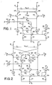
- FIG. l and FIG. 2 which exemplify different wideband amplifiers employing the active RC network of the present invention.
- transistors Ql, Q2, Q3, and Q4 comprise a cascode differential amplifier wherein the emitters of transistors Ql and Q2 are coupled together through a suitable resistor l0 having a value R E1 , and the collectors of transistors Ql and Q2 are coupled to the emitters of common-base amplifier output transistors Q3 and Q4, respectively.
- the emitters of transistors Ql and Q2 are also returned through respective current sinks l2 and l4 to a suitable negative voltage supply -V.
- the bases of transistors Q3 and Q4 are connected to a suitable bias voltage supply +V BB , while the Q3 and Q4 collectors are connected through respective load resistors l6 and l8 to a suitable positive voltage supply +V.
- An input signal V IN is applied across the bases of transistors Ql and Q2, and an output signal V OUT is taken across the collectors of transistors Q3 and Q4.
- transistors Ql, Q2, Q3, and Q4 comprise an f T doubler differential amplifier wherein the emitters of transistors Ql and Q3 are coupled together through a resistor l0, while the emitters of transistors Q2 and Q4 are coupled together through a resistor l0 ⁇ .
- the emitters of transistors Ql-Q2-Q3-Q4 are also returned through respective current sinks l2-l4-22-24 to the negative supply.
- the bases of transistors Q3 and Q4 are connected to the bias supply voltage.
- the collectors of transistors Ql and Q4 are connected through load resistor l6 to the positive supply voltage on one side of the amplifier, while the collectors of transistors Q2 and Q3 are connected through load resistor l8 to the positive supply voltage on the other side.
- an input signal is applied across the bases of transistors Ql and Q2, while an output signal is taken across the collectors of transistors Ql-Q4 and Q2-Q3.
- an equivalent RC network comprising an emitter-coupled pair of transistors Q5 and Q6, with associated circuit elements, is connected across the emitters of transistors Ql and Q2.
- the base of transistor Q5 is connected to the emitter of transistor Ql
- the base of transistor Q6 is connected to the emitter of transistor Q2
- the emitters of transistors Q5 and Q6 are coupled together through a resistor 30 having a value R E .
- the emitter of transistor Q5 is returned to a suitable source of negative supply voltage -V E through current-sink transistor Q7 and resistor 32, and likewise, the emitter of transistor Q6 is returned to the negative supply through current-sink transistor Q8 and resistor 34.
- the amount of current through transistors Q7 and Q8 is controlled by a diode-connected transistor Q9 and resistor 36 in current-mirror fashion. That is, the bases of transistors Q7, Q8, and Q9 are connnected together to effect control, and the base-to-emitter junction areas of the three transistors are chosen so that the current produced through transistor Q9 is mirrored by a proportional amount in transistors Q7 and Q8.
- the collector of transistor Q9 is connected to a current source 40 to control the amount of current through transistor Q9, and hence, through transistors Q7 and Q8.
- Current source 40 is shown as a variable current source; however, in actual practice, current source 40 may be fixed, or it may be programmable to facilitate automatically setting the standing current levels through transistors Q5 and Q6 thereby to establish the equivalent capacitance value, as will be seen shortly.
- the collectors of transistors Q5 and Q6 are connected through respective load resistors 44 and 46, and a resistor 48 to a suitable source of control voltage V C , represented by a variable voltage generator 50.
- V C a suitable source of control voltage
- voltage generator 50 may be fixed, or it may be programmable to facilitate automatically setting the collector voltage of transistors Q5 and Q6 thereby to set the equivalent capacitance value of the circuit.
- the effective equivalent resistance R of the active RC network is the base resistance of transistors Q5 and Q6, which depends largely on base geometry and the particular process used, and resistor 30.
- the effective equivalent C of the active RC network may be expressed as follows: wherein C o is the base-to-collector capacitance of transistors Q5 and Q6 at zero volts, V a is the collector-to-base voltage of transistors Q5 and Q6, V bi is the built-in base potential of transistors Q5 and Q6, and T T is the reciprocal of f T of transistors Q5 and Q6. Variation of the value of C depends upon the applied collector voltage and f T versus emitter current I E for a given value of resistance R E .
- resistors 44 and 46 may be chosen to provide a specific time-constant compensation.
- the values of V C , I R , and resistor 48 must be carefully selecected so that the collector-base junction of transistors Q5 and Q6 will not be forward biased within the controlling range.
- this compensation circuit is temperature compensated for the beta loading effect of Q5 and Q6 since the reflected resistance (beta plus one, times R E ) is effectively connected across the emitters of the differential amplifier.
- the active compensation circuit of the present invention may easily be implemented in integrated circuit form along with the differential amplifier components to provide an amplifier whose high frequency compensation can be optimally set simply by adjusting either a control current or a control voltage.
Abstract
Description
- A common amplifier configuration used in electronic instruments is the differential amplifier. Typically, such differential amplifiers comprise a pair of transistors having their emitters coupled together via a resistive-capacitive (RC) network, wherein an input signal is applied across the bases of such pair of transistors and an output signal is developed across the collectors. It is a common technique to provide an adjustable capacitor in the RC network to allow adjustment of high-frequency compensation or high-frequency response of the amplifier.
- It has become advantageous for many reasons to implement wideband amplifiers in integrated circuits. Even so, certain circuit elements, also known as discrete components, have had to remain outside the integrated circuit package, either because they cannot be conveniently implemented, or because they involve selection or adjustment as dictated by the operating environment. One such discrete component is the aforementioned adjustable capacitor, which because of associated lead inductance and packaging parasitic capacitances, makes high-frequency adjustments for the amplifier a difficult and often tedious task.
- In accordance with the present invention, a wideband amplifier with active high-frequency compensation includes an active equivalent RC network implemented in an integrated circuit along with differential amplifier components. The active equivalent capacitor portion of the RC network exploits the properties of voltage-dependent junction capacitance of transistors and the equivalent circuit input capacitance of a common-emitter transistor configuration. An optimum amount of capacitance required in the RC network for establishing a desirable high-frequency compensation may be obtained in the present invention by varying either a voltage or a current.
- A specific embodiment of an active equivalent RC network for use in a wideband differential amplifier comprises an emitter-coupled pair of transistors and associated circuitry connected between the emitters of a pair of differential amplifier transistors.
- Advantages and attainments of the present invention will become apparent to those having ordinary skill in the art upon a reading of the following description when taken in conjunction with the accompanying drawings.
-
- FIG. l is a schematic diagram of a cascode amplifier employing the active RC network of the present invention; and
- FIG. 2 is a schematic diagram of an fT doubler amplifier employing the active RC network of the present invention.
- This description will be made with reference to both FIG. l and FIG. 2, which exemplify different wideband amplifiers employing the active RC network of the present invention.
- In FIG. l, transistors Ql, Q2, Q3, and Q4 comprise a cascode differential amplifier wherein the emitters of transistors Ql and Q2 are coupled together through a suitable resistor l0 having a value RE1, and the collectors of transistors Ql and Q2 are coupled to the emitters of common-base amplifier output transistors Q3 and Q4, respectively. The emitters of transistors Ql and Q2 are also returned through respective current sinks l2 and l4 to a suitable negative voltage supply -V. The bases of transistors Q3 and Q4 are connected to a suitable bias voltage supply +VBB, while the Q3 and Q4 collectors are connected through respective load resistors l6 and l8 to a suitable positive voltage supply +V. An input signal VIN is applied across the bases of transistors Ql and Q2, and an output signal VOUT is taken across the collectors of transistors Q3 and Q4.
- In FIG. 2, transistors Ql, Q2, Q3, and Q4 comprise an fT doubler differential amplifier wherein the emitters of transistors Ql and Q3 are coupled together through a resistor l0, while the emitters of transistors Q2 and Q4 are coupled together through a resistor l0ʹ. The emitters of transistors Ql-Q2-Q3-Q4 are also returned through respective current sinks l2-l4-22-24 to the negative supply. The bases of transistors Q3 and Q4 are connected to the bias supply voltage. The collectors of transistors Ql and Q4 are connected through load resistor l6 to the positive supply voltage on one side of the amplifier, while the collectors of transistors Q2 and Q3 are connected through load resistor l8 to the positive supply voltage on the other side. As described above for the cascode configuration, an input signal is applied across the bases of transistors Ql and Q2, while an output signal is taken across the collectors of transistors Ql-Q4 and Q2-Q3.
- For either of the differential amplifier configurations exemplified in FIG. l and FIG.2, an equivalent RC network comprising an emitter-coupled pair of transistors Q5 and Q6, with associated circuit elements, is connected across the emitters of transistors Ql and Q2. The base of transistor Q5 is connected to the emitter of transistor Ql, the base of transistor Q6 is connected to the emitter of transistor Q2, and the emitters of transistors Q5 and Q6 are coupled together through a
resistor 30 having a value RE. The emitter of transistor Q5 is returned to a suitable source of negative supply voltage -VE through current-sink transistor Q7 andresistor 32, and likewise, the emitter of transistor Q6 is returned to the negative supply through current-sink transistor Q8 andresistor 34. The amount of current through transistors Q7 and Q8 is controlled by a diode-connected transistor Q9 andresistor 36 in current-mirror fashion. That is, the bases of transistors Q7, Q8, and Q9 are connnected together to effect control, and the base-to-emitter junction areas of the three transistors are chosen so that the current produced through transistor Q9 is mirrored by a proportional amount in transistors Q7 and Q8. The collector of transistor Q9 is connected to acurrent source 40 to control the amount of current through transistor Q9, and hence, through transistors Q7 and Q8.Current source 40 is shown as a variable current source; however, in actual practice,current source 40 may be fixed, or it may be programmable to facilitate automatically setting the standing current levels through transistors Q5 and Q6 thereby to establish the equivalent capacitance value, as will be seen shortly. - The collectors of transistors Q5 and Q6 are connected through
respective load resistors resistor 48 to a suitable source of control voltage VC, represented by avariable voltage generator 50. Again, in actual practice,voltage generator 50 may be fixed, or it may be programmable to facilitate automatically setting the collector voltage of transistors Q5 and Q6 thereby to set the equivalent capacitance value of the circuit. - The effective equivalent resistance R of the active RC network is the base resistance of transistors Q5 and Q6, which depends largely on base geometry and the particular process used, and
resistor 30. The effective equivalent C of the active RC network may be expressed as follows:
- From the foregoing mathematical expression, it can be discerned that a change in VC or a change in IR can be made to provide a value of capacitance to establish a desirable high-frequency response for the differential amplifier of either FIG. l or FIG. 2.
- The values of
resistors resistor 48 must be carefully selecected so that the collector-base junction of transistors Q5 and Q6 will not be forward biased within the controlling range. - It should be mentioned that another benefit of this compensation circuit is that it is temperature compensated for the beta loading effect of Q5 and Q6 since the reflected resistance (beta plus one, times RE) is effectively connected across the emitters of the differential amplifier.
- The active compensation circuit of the present invention may easily be implemented in integrated circuit form along with the differential amplifier components to provide an amplifier whose high frequency compensation can be optimally set simply by adjusting either a control current or a control voltage.
Claims (4)
a pair of emitter-coupled compensation transistors each having a base connected to an emitter of a respective input transistor, said pair of transistors each having a predetermined base-to-collector capacitance;
means for controlling the conduction of said compensation transistors; and
means for controlling the collector-base voltage of said compensation transistors.
Applications Claiming Priority (2)
| Application Number | Priority Date | Filing Date | Title |
|---|---|---|---|
| US06/855,533 US4703285A (en) | 1986-04-23 | 1986-04-23 | Wideband amplifier with active high-frequency compensation |
| US855533 | 1986-04-23 |
Publications (3)
| Publication Number | Publication Date |
|---|---|
| EP0242439A2 true EP0242439A2 (en) | 1987-10-28 |
| EP0242439A3 EP0242439A3 (en) | 1989-01-25 |
| EP0242439B1 EP0242439B1 (en) | 1992-05-20 |
Family
ID=25321498
Family Applications (1)
| Application Number | Title | Priority Date | Filing Date |
|---|---|---|---|
| EP86116429A Expired - Lifetime EP0242439B1 (en) | 1986-04-23 | 1986-11-26 | Wideband amplifier with active high-frequency compensation |
Country Status (5)
| Country | Link |
|---|---|
| US (1) | US4703285A (en) |
| EP (1) | EP0242439B1 (en) |
| JP (1) | JPS62256504A (en) |
| CA (1) | CA1252526A (en) |
| DE (1) | DE3685436D1 (en) |
Cited By (1)
| Publication number | Priority date | Publication date | Assignee | Title |
|---|---|---|---|---|
| EP0555748A1 (en) * | 1992-02-14 | 1993-08-18 | Robert Bosch Gmbh | Amplifier stage with negative feedback |
Families Citing this family (6)
| Publication number | Priority date | Publication date | Assignee | Title |
|---|---|---|---|---|
| US4897616A (en) * | 1988-07-25 | 1990-01-30 | Burr-Brown Corporation | Wide band amplifier with current mirror feedback to bias circuit |
| DE4004135A1 (en) * | 1990-02-10 | 1991-08-14 | Thomson Brandt Gmbh | FREQUENCY COMPENSATED CIRCUIT |
| JPH07101816B2 (en) * | 1990-06-06 | 1995-11-01 | 工業技術院長 | Phase-locked circuit of ultra-high frequency diode oscillator |
| JPH0794971A (en) * | 1993-09-24 | 1995-04-07 | Mitsubishi Electric Corp | Differential amplifier |
| US6091301A (en) * | 1996-06-03 | 2000-07-18 | Scientific-Atlanta, Inc. | Flatness compensation of diplex filter roll-off using active amplifier peaking circuit |
| US7206234B2 (en) * | 2005-06-21 | 2007-04-17 | Micron Technology, Inc. | Input buffer for low voltage operation |
Citations (3)
| Publication number | Priority date | Publication date | Assignee | Title |
|---|---|---|---|---|
| EP0101201A2 (en) * | 1982-07-19 | 1984-02-22 | Nippon Telegraph And Telephone Corporation | Monolithic integrated circuit device including AC negative feedback type high frequency amplifier circuit |
| GB2151865A (en) * | 1983-12-17 | 1985-07-24 | Toshiba Kk | Semiconductor integrated circuit using vertical pnp transistors |
| US4575687A (en) * | 1984-10-01 | 1986-03-11 | Gould Inc. | Voltage adjustable capacitance for frequency response shaping |
Family Cites Families (3)
| Publication number | Priority date | Publication date | Assignee | Title |
|---|---|---|---|---|
| US4390848A (en) * | 1981-02-12 | 1983-06-28 | Signetics | Linear transconductance amplifier |
| JPS58202605A (en) * | 1982-05-21 | 1983-11-25 | Hitachi Ltd | Cascode amplifier |
| JPS60214610A (en) * | 1984-04-11 | 1985-10-26 | Fujitsu Ltd | Transistor circuit |
-
1986
- 1986-04-23 US US06/855,533 patent/US4703285A/en not_active Expired - Lifetime
- 1986-11-18 CA CA000523225A patent/CA1252526A/en not_active Expired
- 1986-11-26 EP EP86116429A patent/EP0242439B1/en not_active Expired - Lifetime
- 1986-11-26 DE DE8686116429T patent/DE3685436D1/en not_active Expired - Fee Related
-
1987
- 1987-04-13 JP JP62090620A patent/JPS62256504A/en active Granted
Patent Citations (3)
| Publication number | Priority date | Publication date | Assignee | Title |
|---|---|---|---|---|
| EP0101201A2 (en) * | 1982-07-19 | 1984-02-22 | Nippon Telegraph And Telephone Corporation | Monolithic integrated circuit device including AC negative feedback type high frequency amplifier circuit |
| GB2151865A (en) * | 1983-12-17 | 1985-07-24 | Toshiba Kk | Semiconductor integrated circuit using vertical pnp transistors |
| US4575687A (en) * | 1984-10-01 | 1986-03-11 | Gould Inc. | Voltage adjustable capacitance for frequency response shaping |
Cited By (1)
| Publication number | Priority date | Publication date | Assignee | Title |
|---|---|---|---|---|
| EP0555748A1 (en) * | 1992-02-14 | 1993-08-18 | Robert Bosch Gmbh | Amplifier stage with negative feedback |
Also Published As
| Publication number | Publication date |
|---|---|
| DE3685436D1 (en) | 1992-06-25 |
| EP0242439B1 (en) | 1992-05-20 |
| CA1252526A (en) | 1989-04-11 |
| JPS62256504A (en) | 1987-11-09 |
| EP0242439A3 (en) | 1989-01-25 |
| JPH0350447B2 (en) | 1991-08-01 |
| US4703285A (en) | 1987-10-27 |
Similar Documents
| Publication | Publication Date | Title |
|---|---|---|
| US4769619A (en) | Compensated current mirror | |
| US6642741B2 (en) | Electronically adjustable integrated circuit input/output termination method and apparatus | |
| EP0004099B1 (en) | Electrically variable impedance circuit | |
| US4567444A (en) | Current mirror circuit with control means for establishing an input-output current ratio | |
| US4760353A (en) | Integrated gyrator oscillator | |
| US4901031A (en) | Common-base, source-driven differential amplifier | |
| US4409500A (en) | Operational rectifier and bias generator | |
| EP0209987A2 (en) | Unity gain buffer amplifiers | |
| GB2159305A (en) | Band gap voltage reference circuit | |
| US4703285A (en) | Wideband amplifier with active high-frequency compensation | |
| GB2292858A (en) | Bias circuit for low voltage bipolar amplifier | |
| EP0052117B1 (en) | Current mode biquadratic active filter | |
| US4425551A (en) | Differential amplifier stage having bias compensating means | |
| US4187472A (en) | Amplifier employing matched transistors to provide linear current feedback | |
| EP0161067A2 (en) | Voltage follower | |
| US5172017A (en) | Integrated circuit arrangement including a differential amplifier which generates a constant output voltage over a large temperature range | |
| US3541465A (en) | Transistor differential amplifier circuit | |
| US4378529A (en) | Differential amplifier input stage capable of operating in excess of power supply voltage | |
| US4725790A (en) | Broadband DC level shift circuit with feedback | |
| US6614284B1 (en) | PNP multiplier | |
| EP0667057A1 (en) | Active impedance termination | |
| GB2121633A (en) | Improvements in or relating to electronic circuits | |
| EP0337561B1 (en) | Control amplifier | |
| US4006369A (en) | Current generator including a rate discriminator | |
| US6614306B1 (en) | Bias circuit for class AB high frequency amplifiers |
Legal Events
| Date | Code | Title | Description |
|---|---|---|---|
| PUAI | Public reference made under article 153(3) epc to a published international application that has entered the european phase |
Free format text: ORIGINAL CODE: 0009012 |
|
| AK | Designated contracting states |
Kind code of ref document: A2 Designated state(s): DE FR GB NL |
|
| PUAL | Search report despatched |
Free format text: ORIGINAL CODE: 0009013 |
|
| AK | Designated contracting states |
Kind code of ref document: A3 Designated state(s): DE FR GB NL |
|
| 17P | Request for examination filed |
Effective date: 19890330 |
|
| 17Q | First examination report despatched |
Effective date: 19910212 |
|
| GRAA | (expected) grant |
Free format text: ORIGINAL CODE: 0009210 |
|
| AK | Designated contracting states |
Kind code of ref document: B1 Designated state(s): DE FR GB NL |
|
| REF | Corresponds to: |
Ref document number: 3685436 Country of ref document: DE Date of ref document: 19920625 |
|
| ET | Fr: translation filed | ||
| PGFP | Annual fee paid to national office [announced via postgrant information from national office to epo] |
Ref country code: FR Payment date: 19921010 Year of fee payment: 7 |
|
| PGFP | Annual fee paid to national office [announced via postgrant information from national office to epo] |
Ref country code: GB Payment date: 19921016 Year of fee payment: 7 |
|
| PGFP | Annual fee paid to national office [announced via postgrant information from national office to epo] |
Ref country code: DE Payment date: 19921019 Year of fee payment: 7 |
|
| PGFP | Annual fee paid to national office [announced via postgrant information from national office to epo] |
Ref country code: NL Payment date: 19921130 Year of fee payment: 7 |
|
| PLBE | No opposition filed within time limit |
Free format text: ORIGINAL CODE: 0009261 |
|
| STAA | Information on the status of an ep patent application or granted ep patent |
Free format text: STATUS: NO OPPOSITION FILED WITHIN TIME LIMIT |
|
| 26N | No opposition filed | ||
| PG25 | Lapsed in a contracting state [announced via postgrant information from national office to epo] |
Ref country code: GB Effective date: 19931126 |
|
| PG25 | Lapsed in a contracting state [announced via postgrant information from national office to epo] |
Ref country code: NL Effective date: 19940601 |
|
| NLV4 | Nl: lapsed or anulled due to non-payment of the annual fee | ||
| GBPC | Gb: european patent ceased through non-payment of renewal fee |
Effective date: 19931126 |
|
| PG25 | Lapsed in a contracting state [announced via postgrant information from national office to epo] |
Ref country code: FR Effective date: 19940729 |
|
| PG25 | Lapsed in a contracting state [announced via postgrant information from national office to epo] |
Ref country code: DE Effective date: 19940802 |
|
| REG | Reference to a national code |
Ref country code: FR Ref legal event code: ST |