EP0241979B1 - Circuit arrangement for the reduction of an interfering current produced by a load - Google Patents
Circuit arrangement for the reduction of an interfering current produced by a load Download PDFInfo
- Publication number
- EP0241979B1 EP0241979B1 EP87200622A EP87200622A EP0241979B1 EP 0241979 B1 EP0241979 B1 EP 0241979B1 EP 87200622 A EP87200622 A EP 87200622A EP 87200622 A EP87200622 A EP 87200622A EP 0241979 B1 EP0241979 B1 EP 0241979B1
- Authority
- EP
- European Patent Office
- Prior art keywords
- current
- voltage
- load
- circuit
- supply voltage
- Prior art date
- Legal status (The legal status is an assumption and is not a legal conclusion. Google has not performed a legal analysis and makes no representation as to the accuracy of the status listed.)
- Expired - Lifetime
Links
Images

Classifications
-
- H—ELECTRICITY
- H02—GENERATION; CONVERSION OR DISTRIBUTION OF ELECTRIC POWER
- H02M—APPARATUS FOR CONVERSION BETWEEN AC AND AC, BETWEEN AC AND DC, OR BETWEEN DC AND DC, AND FOR USE WITH MAINS OR SIMILAR POWER SUPPLY SYSTEMS; CONVERSION OF DC OR AC INPUT POWER INTO SURGE OUTPUT POWER; CONTROL OR REGULATION THEREOF
- H02M1/00—Details of apparatus for conversion
- H02M1/14—Arrangements for reducing ripples from dc input or output
- H02M1/15—Arrangements for reducing ripples from dc input or output using active elements
Definitions
- the invention relates to a circuit arrangement with a load, which is coupled to a supply voltage source, according to the preamble of the main claim.
- a circuit arrangement is known from EP 00 59 053, in which a supply voltage source, which supplies an alternating voltage, is coupled to a load, a switching power supply, via a filter.
- the switching power supply causes an interference current due to switching operations, the frequency of which is significantly higher than that of the current of the supply voltage source and which has an effect on the supply voltage source.
- the filter consisting of a coil and a capacitor serves to prevent this interference current.
- the coil is connected to the supply voltage source and on the other hand to the load and the capacitor lying parallel to the load.
- the circuit arrangement described therein for reducing an interference current caused in a load contains a compensation circuit which is arranged in a connecting branch between the load and a supply voltage source.
- the compensation circuit comprises a controlled signal source with a capacitor.
- the controlled signal source is designed as a bridge circuit, which contains switching transistors in each branch.
- the switching transistors are controlled by a control circuit so that the transistors arranged in opposite bridge branches are each conductive or blocked.
- the compensation current flows through a transistor and the capacitor to the transistor in the opposite branch.
- Half of the supply voltage drops across a transistor, which means that transistors with a high dielectric strength must be used.
- a voltage divider is connected in parallel with the load and supplies the control circuit with a voltage which is proportional to the interference voltage and the supply voltage.
- the control circuit determines the duration of the conductive or blocked state of a transistor from this voltage. With the help of the bridge circuit, a current largely compensating for the interference current is generated. Due to the non-ideal components in the controlled signal source and the control circuit, the interference current is not fully compensated.
- an active low-pass filter which is connected between a supply voltage source and a load, such as a teleprinter.
- the variable load causes interference currents that are largely compensated for by the active filter.
- the active filter contains a compensation circuit, an inductive element and a capacitive element.
- the interference currents caused by the load are partially eliminated by the inductive and capacitive element.
- a further reduction is achieved through the compensation circuit.
- a measuring resistor that measures in a supply line is arranged between the supply voltage source and the compensation circuit, the existing interference current, which is fed to a voltage-current converter via a voltage amplifier.
- the voltage-current transformer generates a compensation current that counteracts the existing interference current. A direct current is superimposed on this compensation current because the compensation circuit is supplied with energy by the supply voltage source.
- the invention has for its object to provide a circuit arrangement of the type mentioned which contains a simply designed compensation circuit which brings about a substantial reduction in the interference current.
- a current is conducted into the capacitor with the circuit, which corresponds approximately to the interference current in terms of phase and size.
- the interference current is largely conducted through the controlled signal source via the capacitor, so that only a small proportion of the interference current can reach the supply voltage source.
- the control signal that is supplied to the signal source depends on the interference current.
- the control signal is obtained here by means of two measuring resistors and the amplifier circuit.
- the current that flows through the first measuring resistor contains the total Interference current.
- a current flows in the second measuring resistor which still has a small proportion of the interference current.
- the currents flowing through the two measuring resistors cause a voltage drop. These voltages are subtracted from each other in the amplifier circuit and form the control signal for the controlled signal source.
- the second measurement on the second measuring resistor results in a further reduction in the interference current.
- the voltage difference between the voltage at the load and the voltage at the output of the controlled switching source drops, which is usually an order of magnitude smaller than the voltage at the load.
- the transistors used in the controlled signal source therefore do not need to have a dielectric strength that corresponds to the voltage at the load.
- the capacitor 11 is connected in series with the base-emitter path of the replacement transistor. Its base-collector path is bridged by the resistor 27.
- a resistor 25 leads to the base terminal of the replacement transistor, ie to one terminal of capacitor 11, and voltage source 19 is also connected with its negative pole to this terminal 3. The positive pole of the voltage source 19 is at the collector terminal of the replacement transistor.
- the voltage ripple at the load 9 is compensated for by a series regulator.
- the resistor 21 is in series with the load 9 and the entire load current flows through it. Since the resistor 21 has a significant amount, there is the problem of a very poor efficiency, as with all series regulators.
- a current flows through capacitor 11 and increases the base current set by the voltage divider from resistors 25 and 27 through the replacement transistor.
- the transistor current thereby increased (in the collector-emitter path of the replacement transistor) causes a larger voltage drop across the resistor 21.
- the change in voltage across the capacitor 7, which is attributable to the ripple, is therefore not noticeable at the load 9.
- a circuit arrangement is known from French patent application 21 32 235, which likewise does not provide any suggestion for solving the present problem.
- the circuit described there can only be used with sources of lower voltages, e.g. Battery chargers occur.
- sources of lower voltages e.g. Battery chargers occur.
- higher losses occur in particular in the output stage of the amplifier G due to a direct current component of the current i.
- the output stage of the amplifier is designed here as a "class A amplifier", which naturally has higher losses.
- the teaching according to the present application also enables the low-loss compensation of interference currents in supply sources with high supply voltages.
- the circuit arrangement according to the invention can either contain one or more connection branches.
- a current is conducted into the capacitor connected to the signal source, which largely corresponds to the interference current measured in a supply line.
- Part of the interference current is largely derived in each connection branch, so that only a small proportion of the interference current can reach the supply voltage source.
- the control signal that of the respective signal source supplied depends on the current in a supply line. It is not necessary that this dependency be linear.
- an active low-pass filter is known from US Pat. No. 3,414,824, which is connected between a supply voltage source and a variable load, for example a teleprinter.
- the variable load causes interference currents that are largely compensated for by the active filter.
- the active filter contains a compensation circuit, an inductive element and a capacitive element.
- the interference currents caused by the load are largely from the inductive and capacitive element eliminated.
- a further reduction is achieved through the compensation circuit.
- a measuring resistor measures the existing interference current, which is fed to a voltage-current converter via a voltage amplifier.
- the voltage-current transformer generates a counter current, which counteracts the existing interference current. A direct current is superimposed on this counter current.
- the compensation circuit is supplied with energy by the supply voltage source. For this reason, a direct current is superimposed on the counter current. As a result, in addition to the losses occurring in the inductive and capacitive elements, there are additional high losses.
- the supply voltage source can in principle only be a DC voltage source since it supplies the compensation circuit with energy.
- the direct component is suppressed by a capacitor in the connecting branch.
- most of the voltage across the load drops across this capacitor.
- the compensation circuit generates a current opposite to the interference current without a DC component. With this implementation, the losses in the compensation circuit are very much lower than in US Pat. No. 3,414,824.
- the compensation circuit is also not supplied with energy by the supply voltage source, but receives it from an external energy source. If the load is designed as a switching power supply, the compensation circuit can receive the energy from the load.
- the circuit arrangement has only one connecting branch, it is provided that from a first Measuring resistor, which is arranged in a supply line between the load and the series circuit comprising the capacitor and the signal source, the voltage drop the control signal is obtained.
- the voltage across the measuring resistor is dependent on the current supplied by the supply voltage source and the interference current caused by the load.
- an amplifier circuit is supplied with the voltage dropping across the first measuring resistor at its first input and a reference voltage at its second input, which approximately corresponds to the time profile of the current of the supply voltage source , forms an output voltage that represents the control signal.
- a signal which is independent of the current of the supply voltage source can also be obtained by means of a capacitor which is arranged between the measuring resistor and the controlled signal source. The capacitance of the capacitor must be chosen so that it suppresses the low-frequency signal caused by the current of the supply voltage source.
- the reference voltage is obtained from a second measuring resistor, which is arranged between the supply voltage source and the connecting branch and on which the residual interference current remaining due to the incomplete compensation of the interference current is also measured.
- the compensation circuit contains at least two connecting branches, that first measuring resistors are arranged in a feed line in each case between the connecting branches and between the load and a connecting branch and that the control signal for the respective signal source is obtained from the voltage drop in the respective first measuring resistor.
- the current of the supply voltage source is measured with the interference current in the first measuring resistors.
- the voltage across the first measuring resistors is dependent on the current supplied by the supply voltage source and the interference current caused by the load.
- each signal source is assigned an amplifier circuit which is supplied with the voltage dropping at the respective first measuring resistor at its first input and a reference voltage at its second input is, which approximately corresponds to the time course of the current of the supply voltage source, and which forms an output voltage which represents the control signal.
- a signal independent of the current of the supply voltage source could be obtained instead of the amplifier circuit by means of a capacitor which is arranged between the respective first measuring resistor and the respective controlled signal source. The capacitance of the capacitor must be selected so that it suppresses the low-frequency signal caused by the current of the supply voltage source.
- the comparison voltage for the respective amplifier circuit can be obtained at second measuring resistors, which are each arranged in a supply line between the connecting branches and between the supply voltage source and a connecting branch and which are each connected to a connecting branch and a first measuring resistor at which the other input voltage of the amplifier circuit falls off.
- each controlled signal source it is provided that it comprises a power amplifier with a complementary output stage.
- the invention can be used in such a circuit arrangement which contains a switching power supply as a load.
- the circuit arrangement according to FIG. 1 has a supply voltage source 1 which e.g. outputs a DC voltage of 50 V.
- a DC voltage only has a portion at a frequency of zero.
- the supply voltage source l supplies a load 2 via feed lines, which e.g. can be a switching power supply designed as an up-voltage converter. Switching power supplies of this type are generally operated at switching frequencies of approximately 20 kHz to 200 kHz. These switching processes cause an interference current in the input current of the supply voltage source 1, the frequency spectrum of which has components in the switching frequency and its harmonics.
- a compensation circuit which contains a capacitor 3, a controlled signal source 4 and an amplifier circuit 5.
- the current Ya that flows through the load and that contains the interference current, causes a voltage drop across a measuring resistor l0.
- the resistor l0 should preferably be selected such that it is as small as possible on the one hand to limit the losses occurring on it, but on the other hand the voltage drop across it has a sufficiently high level for driving the amplifier circuit 5.
- the measuring resistor l0 is arranged between the negative reference point of the supply voltage source l and a connection point of the load 2.
- the amplifier circuit 5 is connected at the connection point between the load 2 and the measuring resistor 10.
- the amplifier circuit 5 contains an amplifier 11, the inverting input of which is connected to the connection point mentioned above via a resistor l2 and to its output via a resistor l3.
- a resistor l4 connected to the negative reference point of the supply voltage source l and a resistor l5 connected to a reference voltage source Uref are connected to the non-inverting input of the amplifier 11.
- the amplifier circuit 5 contains an amplifier 16, the non-inverting input of which is connected to the negative reference point and the inverting input of which is connected to the output of the amplifier 11 via a resistor 17 and to its output via a resistor 18.
- the output of the amplifier 16 forms the output of the amplifier circuit 5.
- the difference between the reference voltage at the non-inverting input of the amplifier 11, which is an image of the voltage supplied by the supply voltage source 1, and the voltage drop across the first measuring resistor is formed.
- the voltage at the output of the amplifier circuit 5 is dependent on that generated by the load 2 Interference current.
- the resistors l2 to l5 and l7, l8 and the reference voltage Uref, which is an order of magnitude smaller than the DC voltage of the supply voltage source 1, can be chosen so that there is a DC matching of the amplification circuit 5 and the following controlled signal source 4.
- the controlled signal source 4 contains a power amplifier with a complementary output stage of class AB.
- the complementary output stage contains an NPN transistor 20 and a PNP transistor 2l.
- the collector of the transistor 2l is connected to the negative reference point of the supply voltage source l and the base on the one hand to a resistor 22 connected to the negative reference point and on the other hand to the cathode of a diode 23.
- the anode of the diode 23 is on the one hand connected to the output of the amplifier circuit 5, which supplies the control voltage, and on the other hand connected to the cathode of a diode 24.
- the base of transistor 20 is connected to the connection point between the anode of diode 24 and a resistor 25.
- a supply voltage Ub which is an order of magnitude lower than the DC voltage of the supply voltage source 1, is applied to the collector of the transistor 20 and to the other connection point of the resistor 25.
- the emitters of the two transistors 20 and 2l are connected via a connection point to the capacitor 3, which in turn is connected to the positive connection point of the supply voltage source l.
- the controlled signal source 4 drives a current Yc, which is approximately equal to the interference current, through the capacitor 3.
- the transistor 20 or the transistor 2l is conductive. If transistor 20 is conductive, the required current Yc is drawn from the voltage source, which supplies the voltage Ub and which is connected to the ground connection of the supply voltage source 1, which is not shown here. If the transistor 20 is conductive, the current Yc flows through it to the negative reference point.
- the capacitor 3 prevents the DC voltage of the controlled signal source from acting on the supply voltage source 1 and the load 2. The voltage difference across the capacitor 3 drops between the voltage at the load 2 and the voltage at the output of the signal source 4, which is generally an order of magnitude smaller than the voltage at the load 2.
- FIG. 2 one possibility is shown of how a further reduction of the interference current can be achieved.
- the circuit elements with the same functions as in Fig. 1 are provided with the same reference numerals.
- a difference in the exemplary embodiment of FIG. 2 arises in comparison to the exemplary embodiment according to FIG. 1 only in the amplifier circuit 5.
- the resistor 12 is connected, which on the other hand is connected to the inverting input of the amplifier 11 is.
- the inverting input is connected to its output via the resistor l3.
- the non-inverting input is connected to the negative connection of the supply voltage source 1.
- the amplifier 11 At the non-inverting input of the amplifier 11 there is a voltage which drops across a second measuring resistor 30 which is between the negative connection of the supply voltage source 1 and the first measuring resistor l0 is arranged.
- the negative connection of the voltage source Ub from which both the signal source 4 and the amplifiers 11 and 16 are supplied, is connected to the connection point between the two measuring resistors 10 and 30.
- the further structure of the amplifier circuit 5 is identical to the structure according to the exemplary embodiment in FIG. 1.
- the difference between the voltage across the measuring resistor l0 and the voltage across the measuring resistor 30 is formed in the amplifier circuit 5 in accordance with the exemplary embodiment in FIG. 2.
- connection branches are used.
- the example according to FIG. 3 has a supply voltage source 10, which for example emits a DC voltage of 50 V.
- the direct voltage supplied by the supply voltage source 10l only has parts at a frequency of zero.
- the supply voltage source l0l supplies a load l02 via feed lines, which can be, for example, a switching power supply designed as an step-up voltage converter. Switching power supplies of this type are generally operated at switching frequencies of approximately 20 kHz to 200 kHz. These switching processes cause an interference current in the input current of the supply voltage source l0l, the frequency spectrum of which has components at the switching frequency and its harmonics.
- a compensation circuit which contains a first connecting branch with a capacitor l03, with a controlled signal source l04 and with an amplifier circuit l05 and a second connecting branch with a capacitor l06, with a controlled signal source l07 and with an amplifier circuit l08.
- the current Ya which flows through the load and which contains the interference current causes a voltage drop across a measuring resistor 11.
- the measuring resistor ll0 should preferably be chosen so that it is as small as possible to limit the losses that arise on the one hand, but on the other hand the voltage drop across it has a sufficiently high level to control the amplifier circuit l05.
- This resistor ll0 is connected on the one hand to a connection point of the load l02 and on the other hand to a second measuring resistor l30 connected to the negative connection point of the supply voltage source l0l.
- the connection point between the two measuring resistors ll0 and l30 is referred to as the reference point of the first connecting branch.
- the amplifier circuit l05 is connected at the connection point between the load l02 and the measuring resistor ll0.
- the amplifier circuit l05 contains an amplifier lll, the inverting input of which is connected via a resistor ll2 to the connection point mentioned above and via a resistor ll3 to its output.
- a resistor ll4 connected to the reference point of the first connecting branch and a resistor ll5 connected to a reference voltage source Uref are connected to the non-inverting input of the amplifier III.
- amplifier circuit 106 contains an amplifier 116, whose non-inverting input is at the reference point of the first Connection branch is laid and its inverting input is connected via a resistor ll7 to the output of the amplifier III and via a resistor ll8 to its output.
- the output of amplifier ll6 forms the output of amplifier circuit l05.
- the difference between the voltage at the measuring resistor ll0 and a reference voltage at the non-inverting input of the amplifier lll is formed in the amplifier circuit l05, which is an image of the direct voltage supplied by the supply voltage source l0l.
- the voltage at the output of the amplifier circuit l05 depends on the interference current generated by the load l02.
- the resistors ll2 to ll5 and ll7, ll8 and the reference voltage Uref which is an order of magnitude smaller than the DC voltage of the supply voltage source l0l, can be selected so that there is a DC matching of the amplification circuit l05 and the following controlled signal source l04.
- the controlled signal source l04 contains a power amplifier with a complementary output stage of class AB.
- the complementary output stage comprises an NPN transistor l20 and a PNP transistor l2l.
- the collector of the transistor l2l is connected to the reference point of the first connection branch and the base is connected on the one hand to a resistor l22 connected to the reference point of the first connection branch and on the other hand to the cathode of a diode l23.
- the anode of the diode l23 is connected on the one hand to the output of the amplifier circuit l05, which supplies the control voltage, and on the other hand to the cathode of a diode l24.
- the base of the transistor I20 is connected to the connection point between the anode of the diode I24 and a resistor I25.
- a supply voltage Ub that is an order of magnitude lower is than the DC voltage of the supply voltage source l0l, is connected to the collector of the transistor l20 and to the other connection point of the resistor l25.
- the emitters of the two transistors l20 and l2l are connected via a connection point to the capacitor l03, which in turn is connected to the positive connection point of the supply voltage source l0l.
- the controlled signal source l04 drives a current Yc, which is approximately equal to the interference current, through the capacitor l03 depending on the output voltage supplied by the amplifier circuit l05.
- a current Yc which is approximately equal to the interference current
- transistor l20 or transistor l2l is conductive. If the transistor l20 is conductive, the required current Yc is drawn from the voltage source, which supplies the voltage Ub and is connected to the negative connection point of the supply voltage source l0l, which is not shown here. If the transistor l2l is conductive, the current Yc flows through it to the reference point of the first connection branch.
- the capacitor l03 prevents the DC voltage of the controlled signal source from acting on the supply voltage source l0l and the load. The voltage difference across the capacitor l03 drops between the voltage at the load l02 and the voltage at the output of the signal source l04, which is generally an order of magnitude smaller than the voltage at the load 2.
- the interference current which has not been derived via the capacitor l03, will be referred to as partial interference current in the following.
- This Partial interference current causes a voltage drop in measuring resistor l30.
- the measuring resistor l30 should be selected according to the same criteria as the measuring resistor ll0.
- the amplifier circuit 108 is connected to the negative reference point of the first connection branch.
- the amplifier circuit l08 contains an amplifier l3l, the inverting input of which is connected via a resistor l32 to the negative reference point of the first connecting branch and via a resistor l33 to its output.
- a resistor l34 connected to the negative reference point of the supply voltage source l0l and a resistor l35 connected to the reference voltage source Uref are connected to the non-inverting input of the amplifier l3l.
- an amplifier l36 is present in the amplifier circuit l08, the non-inverting input of which is connected to the negative connection of the supply voltage source l0l and the inverting input of which is connected via a resistor l37 to the output of the amplifier l3l and via a resistor l38 to its output.
- the output of amplifier circuit l08 is also the output of amplifier l36.
- the amplifier circuit l08 controls a controlled signal source l07, which comprises a power amplifier with a complementary output stage of class AB.
- the complementary output stage contains an NPN transistor l40 and a PNP transistor l4l.
- the collector of the transistor l40 is connected to the supply voltage Ub and connected to a resistor l42, the other connection point of which is connected to the base of the transistor l40 and to the anode of a diode l43.
- the cathode of diode I43, the anode of a diode I44 and the output of amplifier I36 are connected to a common connection point.
- the cathode of the diode l44 is connected to the one negative connection of the supply voltage source l0l connected resistor l45 and connected to the base of the transistor l4l.
- the collector of the transistor l4l is connected to the negative terminal of the supply voltage source l0l.
- the interconnected emitters of transistors l40 and l4l are connected via capacitor l06 to the positive connection point of supply voltage source l0l.
- the operation of the second connection branch which contains the amplifier circuit l08, the controlled signal source l07 and the capacitor l06, is the same as described above in the explanation of the first connection branch.
- the partial interference current is largely derived through the capacitor l06. A further reduction in the residual interference current can be achieved with one or more further connection branches.
- the remaining interference current can be reduced further by a measure that does not require any further connection branch.
- This possibility is shown in an exemplary embodiment, which is shown in FIG. 4.
- the circuit elements with the same functions as in Fig. 3 are provided with the same reference numerals.
- a difference in the exemplary embodiment in FIG. 4 arises in comparison to the example in accordance with FIG. 3 only in the amplifier circuit 105 and 108.
- the resistor ll2 is connected, which on the other hand is connected to the inverting input of the amplifier lll.
- the inverting input is connected to its output via resistor ll3.
- the non-inverting input is connected to the connection point between the measuring resistor l30 and a further measuring resistor l50, which on the other hand is connected with the connection point of the resistor ll0 facing away from the load l02 is connected.
- the further construction of the amplifier circuit l05 is identical to the construction according to the example in FIG. 3. At the non-inverting input of the amplifier lll there is a voltage which drops across the measuring resistor l50. This voltage is proportional to the current flowing through this resistor 150.
- the voltage across the measuring resistor l50 which is proportional to the current of the voltage source l0l and a low partial interference current, is used to generate the comparison voltage on the one hand and to further reduce the partial interference current on the other hand.
- the resistor l32 is connected to the connection point between the two resistors l30 and l50.
- This resistor l32 and the resistor l33 which is connected with its other connection to the output of the amplifier l3l, are connected to the inverting input of the amplifier l3l.
- the non-inverting input of the amplifier l3l is connected to the negative connection point of the supply voltage source l0l.
- a measuring resistor l5l is connected between the negative connection point of the supply voltage source l0l and the connection point of the resistor l30, which has no connection to the resistor l50.
- the further structure of the amplifier circuit 108 is identical to the structure according to the example in FIG. 3.
- the voltage drop across this measuring resistor l5l is proportional to the current flowing through this resistor.
- the resistor l5l has the same function as the resistor l50.
- the resistor l30 can be omitted if the resistor l32 is not connected between the two resistors l30 and l50, as shown in FIG. 4, but between the resistors l50 and ll0.
- the circuit arrangement according to the invention is not limited to the use of a supply voltage source which supplies a DC voltage, but can also be used if a supply voltage source supplies an AC voltage.
- the parts of the AC voltage source must be at much lower frequencies than the parts of the interference current.
Description
Die Erfindung betrifft eine Schaltungsanordnung mit einer Last, die mit einer Speisespannungsquelle gekoppelt ist, gemäß dem Oberbegriff des Hauptanspruchs.The invention relates to a circuit arrangement with a load, which is coupled to a supply voltage source, according to the preamble of the main claim.
Aus der EP 00 59 053 ist eine Schaltungsanordnung bekannt, in der eine Speisespannungsquelle, die eine Wechselspannung liefert, über ein Filter mit einer Last, einem Schaltnetzteil, gekoppelt ist. Das Schaltnetzteil verursacht aufgrund von Schaltvorgängen einen Störstrom, dessen Frequenz wesentlich höher ist als die des Stromes der Speisespannungsquelle und der auf die Speisespannungsquelle zurückwirkt. Zur Verhinderung dieses Störstromes dient das aus einer Spule und einem Kondensator bestehende Filter. Einerseits ist die Spule an die Speisespannungsquelle und andererseits mit der Last und dem parallel zur Last liegenden Kondensator verbunden. Durch die Verwendung einer Spule zur Reduzierung des Störstromes wird eine wesentliche Verkleinerung der Schaltungsanordnung verhindert.A circuit arrangement is known from EP 00 59 053, in which a supply voltage source, which supplies an alternating voltage, is coupled to a load, a switching power supply, via a filter. The switching power supply causes an interference current due to switching operations, the frequency of which is significantly higher than that of the current of the supply voltage source and which has an effect on the supply voltage source. The filter consisting of a coil and a capacitor serves to prevent this interference current. On the one hand the coil is connected to the supply voltage source and on the other hand to the load and the capacitor lying parallel to the load. By using a coil to reduce the interference current, a substantial downsizing of the circuit arrangement is prevented.
Aus der US-PS 38 25 815 ist ein elektrisches Energieversorgungssystem bekannt. Die darin beschriebene Schaltungsanordnung zur Verringerung eines in einer Last hervorgerufenen Störstromes enthält eine Kompensationsschaltung, welche in einem Verbindungzweig zwischen Last und einer Speisespannungsquelle angeordnet ist. Die Kompensationsschaltung umfaßt eine gesteuerte Signalquelle mit einem Kondensator. Die gesteuerte Signalquelle ist als Brückenschaltung ausgebildet, die in jedem Zweig Schalttransistoren enthält. Die Schalttransistoren werden von einer Steuerschaltung so angesteuert, daß die in gegenüberliegenden Brückenzweigen angeordneten Transistoren jeweils leitend bzw. gesperrt sind. Der Kompensationsstrom fließt über einen Transistor und den Kondensator zum Transistor im gegenüberliegenden Zweig. An einem Transistor fällt die halbe Speisespannung ab, wodurch Transistoren mit einer hohen Spannungsfestigkeit verwendet werden müssen. Parallel zur Last ist ein Spannungsteiler geschaltet, der der Steuerschaltung eine Spannung liefert, welche der Störspannung und der Speisespannung proportional ist. Die Steuerschaltung ermittelt aus dieser Spannung die Dauer des leitenden bzw. gesperrten Zustandes eines Transistors. Mit Hilfe der Brückenschaltung wird ein den Störstrom weitgehend kompensierender Strom erzeugt. Bedingt durch die nichtidealen Bauelemente in der gesteuerten Signalquelle und der Steuerschaltung wird der Störstrom nicht vollständig kompensiert.From US-PS 38 25 815 an electrical power supply system is known. The circuit arrangement described therein for reducing an interference current caused in a load contains a compensation circuit which is arranged in a connecting branch between the load and a supply voltage source. The compensation circuit comprises a controlled signal source with a capacitor. The controlled signal source is designed as a bridge circuit, which contains switching transistors in each branch. The switching transistors are controlled by a control circuit so that the transistors arranged in opposite bridge branches are each conductive or blocked. The compensation current flows through a transistor and the capacitor to the transistor in the opposite branch. Half of the supply voltage drops across a transistor, which means that transistors with a high dielectric strength must be used. A voltage divider is connected in parallel with the load and supplies the control circuit with a voltage which is proportional to the interference voltage and the supply voltage. The control circuit determines the duration of the conductive or blocked state of a transistor from this voltage. With the help of the bridge circuit, a current largely compensating for the interference current is generated. Due to the non-ideal components in the controlled signal source and the control circuit, the interference current is not fully compensated.
Aus der US-PS 34 14 824 ist ein aktives Tiefpaßfilter bekannt, welches zwischen einer Speisespannungsquelle und einer Last, z.B. einem Fernschreiber, geschaltet ist. Die variable Last verursacht Störströme, die von dem aktiven Filter weitgehend kompensiert werden. Das aktive Filter enthält eine Kompensationsschaltung, ein induktives Element und ein kapazitives Element. Die von der Last verursachten Störströme werden teilweise von dem induktiven und kapazitiven Element beseitigt. Eine weitere Reduzierung wird durch die Kompensationsschaltung erreicht. In dieser Kompensationsschaltung mißt ein Meßwiderstand, der in einer Zuleitung zwischen speisespannungsquelle und Kompensationsschaltung angeordnet ist, den vorhandenen Störstrom, der über einen Spannungsverstärker einem Spannungs-Stromwandler zugeführt wird. Der Spannungs-Stromwandler erzeugt einen Kompensationsstrom, der dem vorhandenen Störstrom entgegenwirkt. Diesem Kompensationsstrom ist ein Gleichstrom überlagert, weil die Kompensationsschaltung von der Speisespannungsquelle mit Energie versorgt wird.From US-PS 34 14 824 an active low-pass filter is known, which is connected between a supply voltage source and a load, such as a teleprinter. The variable load causes interference currents that are largely compensated for by the active filter. The active filter contains a compensation circuit, an inductive element and a capacitive element. The interference currents caused by the load are partially eliminated by the inductive and capacitive element. A further reduction is achieved through the compensation circuit. In this compensation circuit, a measuring resistor that measures in a supply line is arranged between the supply voltage source and the compensation circuit, the existing interference current, which is fed to a voltage-current converter via a voltage amplifier. The voltage-current transformer generates a compensation current that counteracts the existing interference current. A direct current is superimposed on this compensation current because the compensation circuit is supplied with energy by the supply voltage source.
Der Erfindung liegt die Aufgabe zugrunde, eine Schaltungsanordnung der eingangs genannten Art zu schaffen, die eine einfach ausgebildete Kompensationsschaltung enthält, welche eine weitgehende Reduktion des Störstromes bewirkt.The invention has for its object to provide a circuit arrangement of the type mentioned which contains a simply designed compensation circuit which brings about a substantial reduction in the interference current.
Diese Aufgabe wird durch die Merkmale des kennzeichnenden Teils des Anspruches 1 gelöst.This object is achieved by the features of the characterizing part of claim 1.
Bei der erfindungsgemäßen Schaltungsanordnung wird mit der Schaltung ein Strom in den Kondensator geleitet, der ungefähr nach Phase und Größe dem Störstrom entspricht. Der Störstrom wird durch die gesteuerte Signalquelle über den Kondensator weitgehend geleitet, so daß nur ein kleiner Anteil des Störstromes zur Speisespannungsquelle gelangen kann. Das Steuersignal, das der Signalquelle zugeführt wird, hängt dabei von dem Störstrom ab. Das Steuersignal wird hierbei mittels zweier Meßwiderstände und der Verstärkerschaltung gewonnen. Der Strom, der durch den ersten Meßwiderstand fließt, enthält den gesamten Störstrom. In dem zweiten Meßwiderstand fließt ein Strom, der noch einen geringen Anteil des Störstromes aufweist. Die Ströme, welche durch die beiden Meßwiderstände fließen, verursachen einen Spannungsfall. Diese Spannungen werden in der Verstärkerschaltung voneinander subtrahiert und bilden das Steuersignal für die gesteuerte Signalquelle. Durch die zweite Messung am zweiten Meßwiderstand ergibt sich eine weitere Verringerung des Störstromes. An dem Kondensator fällt die Spannungsdifferenz zwischen der Spannung an der Last und der Spannung am Ausgang der gesteuerten Schaltquelle ab, die in der Regel eine Größenordnung kleiner ist als die Spannung an der Last. Die in der gesteuerten Signalquelle verwendeten Transistoren brauchen daher keine Spannungsfestigkeit zu haben, die der Spannung an der Last entspricht.In the circuit arrangement according to the invention, a current is conducted into the capacitor with the circuit, which corresponds approximately to the interference current in terms of phase and size. The interference current is largely conducted through the controlled signal source via the capacitor, so that only a small proportion of the interference current can reach the supply voltage source. The control signal that is supplied to the signal source depends on the interference current. The control signal is obtained here by means of two measuring resistors and the amplifier circuit. The current that flows through the first measuring resistor contains the total Interference current. A current flows in the second measuring resistor which still has a small proportion of the interference current. The currents flowing through the two measuring resistors cause a voltage drop. These voltages are subtracted from each other in the amplifier circuit and form the control signal for the controlled signal source. The second measurement on the second measuring resistor results in a further reduction in the interference current. At the capacitor, the voltage difference between the voltage at the load and the voltage at the output of the controlled switching source drops, which is usually an order of magnitude smaller than the voltage at the load. The transistors used in the controlled signal source therefore do not need to have a dielectric strength that corresponds to the voltage at the load.
In der US-PS 38 75 539 ist eine Schaltungsanordnung zum Unterdrücken von einer Hochspannung überlagerten Welligkeiten ("Ripple") bei einer Hochspannungs-Energieversorgung beschrieben. Dieser Schaltung liegt jedoch ein anderes Prinzip zugrunde als der vorliegenden Erfindung. Dies wird deutlich, wenn in der einzigen Figur der US-PS 38 75 539 zur übersichtleren Darstellung alle Schutzelemente, d.h. alle Dioden und die Widerstände mit den dortigen Bezugszeichen 29, 31 und 33 weggelassen werden und die Darlingtonschaltung aus den Transistoren Q1 und Q2, die nur zur höheren Stromverstärkung dient, durch einen einzelnen Transistor ersetzt wird. Zwischen den Anschlüssen 3 und der Quelle 1 liegt dann eine Serienschaltung aus der Last 9 und dem Widerstand 21 vor, zu der parallel der Kondensator 7 geschaltet ist. Parallel zur Last liegt außerdem der Kondensator 11 in Reihe mit der Basis-Emitter-Strecke des Ersatztransistors. Dessen Basis-Kollektor-Strecke wird durch den Widerstand 27 überbrückt. Außerdem führt vom Anschluß 3 der Quelle 1 ein Widerstand 25 an den Basisanschluß des Ersatztransistors, d.h. an den einen Anschluß des Kondensators 11, und außerdem ist die Spannungsquelle 19 mit ihrem negativen Pol an diesem Anschluß 3 angeschlossen. Der positive Pol der Spannungsquelle 19 liegt am Kollektoranschluß des Ersatztransistors.In US-PS 38 75 539 a circuit arrangement for suppressing high-voltage superimposed ripples ("ripple") in a high-voltage power supply is described. However, this circuit is based on a different principle than the present invention. This becomes clear when in the single figure of US-PS 38 75 539 all protective elements, ie all diodes and the resistors with the reference numerals 29, 31 and 33 there are omitted for clarity and the Darlington circuit from the transistors Q1 and Q2, the is used only for higher current gain, is replaced by a single transistor. Between the connections 3 and the source 1 there is then a series connection of the load 9 and the
Bei dieser Schaltungsanordnung wird die Spannungswelligkeit an der Last 9 durch einen Serienregler ausgeglichen. Der Widerstand 21 liegt in Serie zur Last 9 und wird vom gesamten Laststrom durchflossen. Da der Widerstand 21 einen nennenswerten Betrag hat, liegt auch hier wie bei allen Serienreglern das Problem eines sehr schlechten Wirkungsgrades vor. Bei ansteigender Spannung am Kondensator 7 fließt ein Strom durch den Kondensator 11 und vergrößert den durch den Spannungsteiler aus den Widerständen 25 und 27 eingestellten Basisstrom durch den Ersatztransistor. Der dadurch vergrößerte Transistorstrom (in der Kollektor-Emitter-Strecke des Ersatztransistors) ruft einen größeren Spannungsabfall am Widerstand 21 hervor. Damit wird die Spannungsänderung am Kondensator 7, die der Welligkeit zuzurechnen ist, an der Last 9 nicht merkbar.In this circuit arrangement, the voltage ripple at the load 9 is compensated for by a series regulator. The
Das aus der US-PS 38 75 539 bekannt Prinzip kann insgesamt nur zur Kompensation einer Spannungswelligkeit durch Erzeugung einer in Reihe liegenden, gegenphasigen Spannungswelligkeit verwendet werden. Zur verlustarmen Kompensation eines Störstromes durch die Speisequelle, wie sie die Erfindung gemäß der vorliegenden Anmeldung ermöglicht, kann die Schaltungsanordnung gemäß US-PS 38 75 539 nicht herangezogen werden.The principle known from US Pat. No. 3,875,539 can only be used to compensate for a voltage ripple by generating a series-lying voltage ripple in phase opposition. The circuit arrangement according to US Pat. No. 3,875,539 cannot be used for low-loss compensation of an interference current through the supply source, as is made possible by the invention according to the present application.
Aus der französischen Patentanmeldung 21 32 235 ist eine Schaltungsanordnung bekannt, die ebenfalls keine Anregung zur Lösung der vorliegenden Aufgabe liefert. Die dort beschriebene Schaltung ist nämlich nur bei Quellen kleinerer Spannungen anwendbar, wie sie z.B. Batterieladegeräten auftreten. Bei hohen Spannungen treten insbesondere in der Ausgangsstufe des Verstärkers G durch eine Gleichstromkomponente des Stromes i höhere Verluste auf. Außerdem ist hier die Ausgangsstufe des Verstärkers als "Klasse-A-Verstärker" ausgebildet, der naturgemäß höhere Verluste aufweist. Demgegenüber ermöglicht die Lehre gemäß der vorliegenden Anmeldung auch die verlustarme Kompensation von Störströmen bei Speisequellen mit hohen Versorgungsspannungen.A circuit arrangement is known from
Die erfindungsgemäße Schaltungsanordnung kann entweder einen oder mehrere Verbindungszweige enthalten. Mit Hilfe der gesteuerten Signalquelle in jedem Verbindungszweig der Kompensationsschaltung wird ein Strom in den mit der Signalquelle verbundenen Kondensator geleitet, der mit dem in einer Zuleitung gemessenen Störstrom weitgehend übereinstimmt. In jedem Verbindungszweig wird ein Teil des Störstromes weitgehend abgeleitet, so daß nur ein kleiner Anteil des Störstromes zur Speisespannungsquelle gelangen kann. Das Steuersignal, das der jeweiligen Signalquelle zugeführt wird, hängt von dem Strom in einer Zuleitung ab. Es ist nicht notwendig, daß diese Abhängigkeit linear ist.The circuit arrangement according to the invention can either contain one or more connection branches. With the help of the controlled signal source in each connection branch of the compensation circuit, a current is conducted into the capacitor connected to the signal source, which largely corresponds to the interference current measured in a supply line. Part of the interference current is largely derived in each connection branch, so that only a small proportion of the interference current can reach the supply voltage source. The control signal that of the respective signal source supplied depends on the current in a supply line. It is not necessary that this dependency be linear.
Es sei noch erwähnt, daß aus der US-PS 34 14 824 ein aktives Tiefpaßfilter bekannt ist, welches zwischen einer Speisespannungsquelle und einer variablen Last, z.B. einem Fernschreiber, geschaltet wird. Die variable Last verursacht Störströme, die von dem aktiven Filter weitgehend kompensiert werden. Das aktive Filter enthält eine Kompensationsschaltung, ein induktives Element und ein kapazitives Element. Die von der Last verursachten Störströme werden weitgehend von dem induktiven und kapazitiven Element beseitigt. Eine weitere Reduzierung wird durch die Kompensationsschaltung erreicht. In dieser Kompensationsschaltung mißt ein Meßwiderstand den vorhandenen Störstrom, der über einen Spannungsverstärker einem Spannungs-Stromwandler zugeführt wird. Der Spannungs-Stromwandler erzeugt einen Gegenstrom, der dem vorhandenen Störstrom entgegenwirkt. Diesem Gegenstrom ist ein Gleichstrom überlagert. Die Kompensationsschaltung wird von der Speisespannungsquelle mit Energie versorgt. Aus diesem Grund ist dem Gegenstrom ein Gleichstrom überlagert. Hierdurch sind außer den in den induktiven und kapazitiven Element entstehenden Verlusten, zusätzliche hohe Verluste gegeben. Die Speisespannungsquelle kann, da sie die Kompensationsschaltung mit Energie versorgt, prinzipiell nur eine Gleichspannungsquelle sein.It should also be mentioned that an active low-pass filter is known from US Pat. No. 3,414,824, which is connected between a supply voltage source and a variable load, for example a teleprinter. The variable load causes interference currents that are largely compensated for by the active filter. The active filter contains a compensation circuit, an inductive element and a capacitive element. The interference currents caused by the load are largely from the inductive and capacitive element eliminated. A further reduction is achieved through the compensation circuit. In this compensation circuit, a measuring resistor measures the existing interference current, which is fed to a voltage-current converter via a voltage amplifier. The voltage-current transformer generates a counter current, which counteracts the existing interference current. A direct current is superimposed on this counter current. The compensation circuit is supplied with energy by the supply voltage source. For this reason, a direct current is superimposed on the counter current. As a result, in addition to the losses occurring in the inductive and capacitive elements, there are additional high losses. The supply voltage source can in principle only be a DC voltage source since it supplies the compensation circuit with energy.
In der erfindungsgemäßen Schaltungsanordnung wird der Gleichanteil durch einen Kondensator im Verbindungszweig unterdrückt. Außerdem fällt an diesem Kondensator der größte Teil der Spannung an der Last ab. Die Kompensationsschaltung erzeugt hierbei einen dem Störstrom entgegengesetzten Strom ohne einen Gleichanteil. Durch diese Realisierung sind die Verluste in der Kompensationsschaltung sehr viel geringer als in der US-PS 34 14 824. Die Kompensationsschaltung wird außerdem nicht von der Speisespannungsquelle mit Energie versorgt, sondern erhält diese von einer externen Energiequelle. Wenn die Last als Schaltnetzteil ausgebildet ist, kann die Kompensationsschaltung die Energie von der Last erhalten.In the circuit arrangement according to the invention, the direct component is suppressed by a capacitor in the connecting branch. In addition, most of the voltage across the load drops across this capacitor. The compensation circuit generates a current opposite to the interference current without a DC component. With this implementation, the losses in the compensation circuit are very much lower than in US Pat. No. 3,414,824. The compensation circuit is also not supplied with energy by the supply voltage source, but receives it from an external energy source. If the load is designed as a switching power supply, the compensation circuit can receive the energy from the load.
Weist die Schaltungsanordnung nur einen Verbindungszweig auf, so ist vorgesehen, daß aus der an einem ersten Meßwiderstand, der in einer Zuleitung zwischen der Last und der Reihenschaltung aus dem Kondensator und der Signalquelle angeordnet ist, abfallenden Spannung das Steuersignal gewonnen wird.If the circuit arrangement has only one connecting branch, it is provided that from a first Measuring resistor, which is arranged in a supply line between the load and the series circuit comprising the capacitor and the signal source, the voltage drop the control signal is obtained.
Die Spannung an dem Meßwiderstand ist abhängig von dem Strom, der von der Speisespannungsquelle geliefert wird und dem von der Last hervorgerufenen Störstrom. Um ein nur von dem Störstrom abhängiges Signal zu bekommen, ist vorgesehen, daß eine Verstärkerschaltung, der an ihrem ersten Eingang die am ersten Meßwiderstand abfallende Spannung und der an ihrem zweiten Eingang einer Vergleichsspannung zugeführt wird, die dem zeitlichen Verlauf des Stromes der Speisespannungsquelle annähernd entspricht, eine Ausgangsspannung bildet, die das Steuersignal darstellt. Es läßt sich ebenso mittels eines Kondensators, der zwischen dem Meßwiderstand und der gesteuerten Signalquelle angeordnet ist, ein vom Strom der Speisespannungsquelle unabhängiges Signal gewinnen. Die Kapazität des Kondensators muß dabei so gewählt werden, daß er das niederfrequente vom Strom der Speisespannungsquelle hervorgerufene Signal unterdrückt.The voltage across the measuring resistor is dependent on the current supplied by the supply voltage source and the interference current caused by the load. In order to obtain a signal that is only dependent on the interference current, it is provided that an amplifier circuit is supplied with the voltage dropping across the first measuring resistor at its first input and a reference voltage at its second input, which approximately corresponds to the time profile of the current of the supply voltage source , forms an output voltage that represents the control signal. A signal which is independent of the current of the supply voltage source can also be obtained by means of a capacitor which is arranged between the measuring resistor and the controlled signal source. The capacitance of the capacitor must be chosen so that it suppresses the low-frequency signal caused by the current of the supply voltage source.
Die Vergleichsspannung wird an einen zweiten Meßwiderstand gewonnen, der zwischen der Speisespannungsquelle und dem Verbindungszweig angeordnet ist und an dem auch der infolge der nicht vollständigen Kompensation des Störstromes verbleibende restliche Störstrom gemessen wird.The reference voltage is obtained from a second measuring resistor, which is arranged between the supply voltage source and the connecting branch and on which the residual interference current remaining due to the incomplete compensation of the interference current is also measured.
In einer Weiterbildung der Erfindung ist vorgesehen, daß die Kompensationsschaltung mindestens zwei Verbindungszweige enthält, daß erste Meßwiderstände in einer Zuleitung jeweils zwischen den Verbindungszweigen und zwischen der Last und einem Verbindungszweig angeordnet sind und daß aus der in dem jeweiligen ersten Meßwiderstand abfallenden Spannung das Steuersignal für die jeweilige Signalquelle gewonnen wird. In den ersten Meßwiderständen wird der Strom der Speisespannungsquelle mit dem Störstrom gemessen.In a further development of the invention it is provided that the compensation circuit contains at least two connecting branches, that first measuring resistors are arranged in a feed line in each case between the connecting branches and between the load and a connecting branch and that the control signal for the respective signal source is obtained from the voltage drop in the respective first measuring resistor. The current of the supply voltage source is measured with the interference current in the first measuring resistors.
Die Spannung an den ersten Meßwiderständen ist abhängig von dem Strom, der von der Speisespannungsquelle geliefert wird und dem von der Last hervorgerufenen Störstrom. Um ein nur von dem Störstrom abhängiges Signal zu bekommen, ist bei der erfindungsgemäßen Schaltungsanordnung mit mindestens zwei Verbindungszweigen vorgesehen, daß jeder Signalquelle eine Verstärkerschaltung zugeordnet ist, der an ihrem ersten Eingang die am jeweiligen ersten Meßwiderstand abfallende Spannung und an ihrem zweiten Eingang eine Vergleichsspannung zugeführt wird, die dem zeitlichen Verlauf des Stromes der Speisespannungsquelle annähernd entspricht, und die eine Ausgangsspannung bildet, die das Steuersignal darstellt. Auch bei dieser Weiterbildung könnte an Stelle der Verstärkerschaltung mittels eines Kondensators, der zwischen dem jeweiligen ersten Meßwiderstand und der jeweiligen gesteuerten Signalquelle angeordnet ist, ein vom Strom der Speisespannungsquelle unabhängiges Signal gewonnen werden. Die Kapazität des Kondensators muß dabei so gewählt werden, daß er das niederfrequente, vom Strom der Speisespannungsquelle hervorgerufene Signal unterdrückt.The voltage across the first measuring resistors is dependent on the current supplied by the supply voltage source and the interference current caused by the load. In order to obtain a signal that is only dependent on the interference current, it is provided in the circuit arrangement according to the invention with at least two connecting branches that each signal source is assigned an amplifier circuit which is supplied with the voltage dropping at the respective first measuring resistor at its first input and a reference voltage at its second input is, which approximately corresponds to the time course of the current of the supply voltage source, and which forms an output voltage which represents the control signal. In this development too, a signal independent of the current of the supply voltage source could be obtained instead of the amplifier circuit by means of a capacitor which is arranged between the respective first measuring resistor and the respective controlled signal source. The capacitance of the capacitor must be selected so that it suppresses the low-frequency signal caused by the current of the supply voltage source.
Die Vergleichspannung für die jeweilige Verstärkerschaltung kann an zweiten Meßwiderständen gewonnen werden, die jeweils in einer Zuleitung zwischen den Verbindungszweigen und zwischen der Speisespannungsquelle und einem Verbindungszweig angeordnet sind und die jeweils mit einem Verbindungszweig und einem ersten Meßwiderstand verbunden sind, an dem die andere Eingangsspannung der Verstärkerschaltung abfällt.The comparison voltage for the respective amplifier circuit can be obtained at second measuring resistors, which are each arranged in a supply line between the connecting branches and between the supply voltage source and a connecting branch and which are each connected to a connecting branch and a first measuring resistor at which the other input voltage of the amplifier circuit falls off.
In einer Ausführungsform für jede gesteuerte Signalquelle ist vorgesehen, daß dieser einen Leistungsverstärker mit einer komplementären Endstufe umfaßt.In one embodiment for each controlled signal source it is provided that it comprises a power amplifier with a complementary output stage.
Die Erfindung kann in einer solchen Schaltungsanordnung verwendet werden, die als Last ein Schaltnetzteil enthält.The invention can be used in such a circuit arrangement which contains a switching power supply as a load.
Anhand der Zeichnungen wird im folgenden die Erfindung näher erläutert. Es zeigen:
- Fig. l und Fig. 3 zwei Beispiele der grundsätzlichen Schaltungsanordnung und
- Fig. 2 und Fig. 4 zwei Ausführungsbeispiele der erfindungsgemäßen Schaltungsanordnung mit einen bzw. zwei Verbindungszweigen.
- FIGS. 1 and 3 show two examples of the basic circuit arrangement and
- FIGS. 2 and 4 show two exemplary embodiments of the circuit arrangement according to the invention with one or two connecting branches.
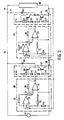
Die Schaltungsanordnung gemäß der Fig. l weist eine Speisespannungsquelle l auf, die z.B. eine Gleichspannung von 50 V abgibt. Eine Gleichspannung hat nur einen Anteil bei einer Frequenz von Null. Die Speisespannungsquelle l versorgt über Zuleitungen eine Last 2, die z.B. ein als Aufwärts-Spannungswandler ausgebildetes Schaltnetzteil sein kann. Derartige Schaltnetzteile werden in der Regel bei Schaltfrequenzen von ungefähr 20 kHz bis 200 kHz betrieben. Diese Schaltvorgänge rufen einen Störstrom im Eingangsstrom der Speisespannungsquelle l hervor, dessen Frequenzspektrum Anteile bei der Schaltfrequenz und deren Harmonischen aufweist.The circuit arrangement according to FIG. 1 has a supply voltage source 1 which e.g. outputs a DC voltage of 50 V. A DC voltage only has a portion at a frequency of zero. The supply voltage source l supplies a
Zur Verringerung dieses Störstromes ist eine Kompensationsschaltung vorgesehen, die einen Kondensator 3, eine gesteuerte Signalquelle 4 und eine Verstärkerschaltung 5 enthält. Der Strom Ya, der durch die Last fließt und der den Störstrom enthält, ruft an einem Meßwiderstand l0 einen Spannungsabfall hervor. Der Widerstand l0 sollte vorzugsweise so gewählt werden, daß er einerseits zur Begrenzung der an ihm entstehenden Verluste möglichst klein ist, andererseits aber die an ihm abfallende Spannung einen genügend hohen Pegel zur Ansteuerung der Verstärkerschaltung 5 aufweist. Der Meßwiderstand l0 ist zwischen dem negativen Bezugspunkt der Speisespannungsquelle l und einem Anschlußpunkt der Last 2 angeordnet. Am Verbindungspunkt zwischen der Last 2 und dem Meßwiderstand l0 ist die Verstärkerschaltung 5 angeschlossen. Die Verstärkerschaltung 5 enthält einen Verstärker ll, dessen invertierender Eingang über einen Widerstand l2 mit dem oben erwähnten Verbindungspunkt und über einen Widerstand l3 mit seinem Ausgang verbunden ist. An dem nichtinvertierenden Eingang des Verstärkers ll ist ein mit dem negativen Bezugspunkt der Speisespannungsquelle l verbundener Widerstand l4 und ein mit einer Referenzspannungsquelle Uref verbundener Widerstand l5 angeschlossen. Des weiteren ist in der Verstärkerschaltung 5 ein Verstärker l6 enthalten, dessen nichtinvertierender Eingang an den negativen Bezugspunkt angeschlossen ist und dessen invertierender Eingang über einen Widerstand l7 mit dem Ausgang des Verstärkers ll und über einen Widerstand l8 mit seinem Ausgang verbunden ist. Der Ausgang des Verstärkers l6 bildet den Ausgang der Verstärkerschaltung 5.To reduce this interference current, a compensation circuit is provided which contains a capacitor 3, a controlled signal source 4 and an amplifier circuit 5. The current Ya that flows through the load and that contains the interference current, causes a voltage drop across a measuring resistor l0. The resistor l0 should preferably be selected such that it is as small as possible on the one hand to limit the losses occurring on it, but on the other hand the voltage drop across it has a sufficiently high level for driving the amplifier circuit 5. The measuring resistor l0 is arranged between the negative reference point of the supply voltage source l and a connection point of the
In der Verstärkerschaltung 5 wird die Differenz zwischen der am nichtinvertierenden Eingang des Verstärkers ll liegenden Vergleichsspannung, die ein Abbild der von der Speisespannungsquelle l gelieferten Spannung ist, und der an dem ersten Meßwiderstand abfallenden Spannung gebildet. Die Spannung am Ausgang der Verstärkerschaltung 5 ist abhängig von dem von der Last 2 erzeugten Störstrom. Die Widerstände l2 bis l5 und l7, l8 und die Referenzspannung Uref, die eine Größenordnung kleiner ist als die Gleichspannung der Speisespannungsquelle l, können so gewählt werden, daß eine gleichspannungsmäßige Anpassung der Verstärkungsschaltung 5 und der folgenden gesteuerten Signalquelle 4 vorhanden ist.In the amplifier circuit 5, the difference between the reference voltage at the non-inverting input of the amplifier 11, which is an image of the voltage supplied by the supply voltage source 1, and the voltage drop across the first measuring resistor is formed. The voltage at the output of the amplifier circuit 5 is dependent on that generated by the
Die gesteuerte Signalquelle 4 enthält einen Leistungsverstärker mit einer komplementären Endstufe der Klasse AB. Die komplementäre Endstufe enthält einen NPN-Transistor 20 und einen PNP-Transistor 2l. Der Kollektor des Transistors 2l ist an den negativen Bezugspunkt der Speisespannungsquelle l angeschlossen und die Basis einerseits an einen mit dem negativen Bezugspunkt verbundenen Widerstand 22 und andererseits an die Kathode einer Diode 23. Die Anode der Diode 23 ist einerseits mit dem Ausgang der Verstärkerschaltung 5, die die Steuerspannung liefert, und andererseits mit der Kathode einer Diode 24 verbunden. An den Anschlußpunkt zwischen der Anode der Diode 24 und einem Widerstand 25 ist die Basis des Transistors 20 gelegt. Eine Versorgungsspannung Ub, die eine Größenordnung geringer ist als die Gleichspannung der Speisespannungsquelle l, ist an den Kollektor des Transistors 20 und an den anderen Anschlußpunkt des Widerstandes 25 gelegt. Die Emitter der beiden Transistoren 20 und 2l sind über einen Verbindungspunkt mit dem Kondensator 3 verbunden, der wiederum an den positiven Anschlußpunkt der Speisespannungsquelle l gelegt ist.The controlled signal source 4 contains a power amplifier with a complementary output stage of class AB. The complementary output stage contains an
Die gesteuerte Signalquelle 4 treibt abhängig von der von der Verstärkerschaltung 5 gelieferten Ausgangsspannung einen Strom Yc, der ungefähr gleich dem Störstrom ist, durch den Kondensator 3. Abhängig von der angelegten Steuerspannung ist entweder der Transistor 20 oder der Transistor 2l leitend. Wenn der Transistor 20 leitend ist, wird der erforderliche Strom Yc aus der Spannungsquelle gezogen, die die Spannung Ub liefert und die an den Masseanschluß der Speisespannungsquelle l, was hier nicht näher dargestellt ist, angeschlossen ist. Ist der Transistor 20 leitend, fließt der Strom Yc über diesen an den negativen Bezugspunkt. Der Kondensator 3 verhindert, daß die Gleichspannung der gesteuerten Signalquelle auf die Speisespannungsquelle l und die Last 2 einwirkt. An dem Kondensator 3 fällt die Spannungsdifferenz zwischen der Spannung an der Last 2 und der Spannung am Ausgang der Signalquelle 4 ab, die in der Regel eine Größenordnung kleiner ist als die Spannung an der Last 2.Depending on the output voltage supplied by the amplifier circuit 5, the controlled signal source 4 drives a current Yc, which is approximately equal to the interference current, through the capacitor 3. Depending on the control voltage applied, either the
Bedingt durch die nichtidealen Bauelemente und die Nichtlinearität der Signalquelle 4 wird keine vollständige Kompensation des Störstromes erreicht.Due to the non-ideal components and the non-linearity of the signal source 4, no complete compensation of the interference current is achieved.
In einem Ausführungsbeispiel, das in der Fig. 2 dargestellt ist, wird eine Möglichkeit gezeigt, wie eine weitere Reduzierung des Störstromes erreicht werden kann. Die Schaltungselemente mit den gleichen Funktionen wie in Fig. l sind mit denselben Bezugszeichen versehen. Ein Unterschied im Ausführungsbeispiel der Fig. 2 ergibt sich gegenüber dem Ausführungsbeispiel gemäß der Fig. l nur in der Verstärkerschaltung 5. An der Verbindung des Meßwiderstandes l0 und der Last 2 ist der Widerstand l2 angeschlossen, der andererseits mit dem invertierenden Eingang des Verstärkers ll verbunden ist. Der invertierende Eingang ist über den Widerstand l3 mit seinem Ausgang verbunden. Der nichtinvertierende Eingang ist in diesem Ausführungsbeispiel mit dem negativen Anschluß der Speisespannungsquelle l verbunden. An dem nichtinvertierenden Eingang des Verstärkers ll liegt eine Spannung, die über einem zweiten Meßwiderstand 30 abfällt, der zwischen dem negativen Anschluß der Speisespannungsquelle l und dem ersten Meßwiderstand l0 angeordnet ist. Der negative Anschluß der Spannungsquelle Ub, aus der sowohl die Signalquelle 4 als auch die Verstärker ll und l6 versorgt werden, ist an den Verbindungspunkt zwischen den beiden Meßwiderständen l0 und 30 angeschlossen. Der weitere Aufbau der Verstärkerschaltung 5 ist mit dem Aufbau gemäß dem Ausführungsbeispiel der Fig. l identisch. In der Verstärkerschaltung 5 wird gemäß dem Ausführungsbeispiel der Fig. 2 die Differenz zwischen der Spannung am Meßwiderstand l0 und der Spannung am Meßwiderstand 30 gebildet.In one exemplary embodiment, which is shown in FIG. 2, one possibility is shown of how a further reduction of the interference current can be achieved. The circuit elements with the same functions as in Fig. 1 are provided with the same reference numerals. A difference in the exemplary embodiment of FIG. 2 arises in comparison to the exemplary embodiment according to FIG. 1 only in the amplifier circuit 5. At the connection of the measuring
In einem praktischen Schaltungsaufbau wurde ein Schaltnetzteil verwendet, das einen dreieckförmigen Störstrom hervorruft. Es hat sich gezeigt, daß die erste Harmonische des Störstromes, die bei 20 kHz liegt, gemäß dem Ausführungsbeispiel der Fig. l um 30 dB reduziert wurde und beim Ausführungsbeispiel der Fig. 2 die erste Harmonische um 50 dB reduziert werden konnte.In a practical circuit design, a switched-mode power supply that generates a triangular interference current was used. It has been shown that the first harmonic of the interference current, which is at 20 kHz, was reduced by 30 dB in accordance with the exemplary embodiment in FIG. 1, and in the exemplary embodiment in FIG. 2 the first harmonic could be reduced by 50 dB.
In den Beispielen gemäß der Fig. 3 und der Fig. 4 werden zwei Verbindungszweige verwendet. Das Beispiel gemäß der Fig. 3 weist eine Speisespannungsquelle l0l auf, die z.B. eine Gleichspannung von 50 V abgibt. Die von der Speisespannungsquelle l0l gelieferte Gleichspannung hat nur Anteile bei einer Frequenz von Null. Die Speisespannungsquelle l0l versorgt über Zuleitungen eine Last l02, die z.B. ein als Aufwärts-Spannungswandler ausgebildetes Schaltnetzteil sein kann. Derartige Schaltnetzteile werden in der Regel bei Schaltfrequenzen von ungefähr 20 kHz bis 200 kHz betrieben. Diese Schaltvorgänge rufen einen Störstrom im Eingangsstrom der Speisespannungsquelle l0l hervor, dessen Frequenzspektrum Anteile bei der Schaltfrequenz und deren Harmonischen aufweist.In the examples according to FIG. 3 and FIG. 4, two connection branches are used. The example according to FIG. 3 has a
Zur Verringerung dieses Störstromes ist eine Kompensationsschaltung vorgesehen, die einen ersten Verbindungszweig mit einem Kondensator l03, mit einer gesteuerten Signalquelle l04 und mit einer Verstärkerschaltung l05 und einen zweiten Verbindungszweig mit einem Kondensator l06, mit einer gesteuerten Signalquelle l07 und mit einer Verstärkerschaltung l08 enthält. Der Strom Ya, der durch die Last fließt, und der den Störstrom enthält, ruft an einem Meßwiderstand ll0 einen Spannungsabfall hervor. Der Meßwiderstand ll0 sollte vorzugsweise so gewählt werden, daß er einerseits zur Begrenzung der an ihm entstehenden Verluste möglichst klein ist, andererseits aber die an ihm abfallende Spannung einen genügend hohen Pegel zur Ansteuerung der Verstärkerschaltung l05 aufweist. Dieser Widerstand ll0 ist einerseits an einen Anschlußpunkt der Last l02 und andererseits an einen mit dem negativen Anschlußpunkt der Speisespannungsquelle l0l verbundenen zweiten Meßwiderstand l30 angeschlossen. Im folgenden wird der Anschlußpunkt zwischen den beiden Meßwiderständen ll0 und l30 als Bezugspunkt des ersten Verbindungszweiges bezeichnet.To reduce this interference current, a compensation circuit is provided which contains a first connecting branch with a capacitor l03, with a controlled signal source l04 and with an amplifier circuit l05 and a second connecting branch with a capacitor l06, with a controlled signal source l07 and with an amplifier circuit l08. The current Ya which flows through the load and which contains the interference current causes a voltage drop across a measuring resistor 11. The measuring resistor ll0 should preferably be chosen so that it is as small as possible to limit the losses that arise on the one hand, but on the other hand the voltage drop across it has a sufficiently high level to control the amplifier circuit l05. This resistor ll0 is connected on the one hand to a connection point of the load l02 and on the other hand to a second measuring resistor l30 connected to the negative connection point of the supply voltage source l0l. In the following, the connection point between the two measuring resistors ll0 and l30 is referred to as the reference point of the first connecting branch.
Am Verbindungspunkt zwischen der Last l02 und dem Meßwiderstand ll0 ist die Verstärkerschaltung l05 angeschlossen. Die Verstärkerschaltung l05 enthält einen Verstärker lll, dessen invertierender Eingang über einen Widerstand ll2 mit dem oben erwähnten Verbindungspunkt und über einen Widerstand ll3 mit seinem Ausgang verbunden ist. An den nichtinvertierenden Eingang des Verstärkers lll ist ein mit dem Bezugspunkt des ersten Verbindungszweiges verbundener Widerstand ll4 und ein mit einer Referenzspannungsquelle Uref verbundener Widerstand ll5 gelegt. Des weiteren ist in der Verstärkerschaltung l05 ein Verstärker ll6 enthalten, dessen nichtinvertierender Eingang an dem Bezugspunkt des ersten Verbindungszweiges gelegt ist und dessen invertierender Eingang über einen Widerstand ll7 mit dem Ausgang des Verstärkers lll und über einen Widerstand ll8 mit seinem Ausgang verbunden ist. Der Ausgang des Verstärkers ll6 bildet den Ausgang der Verstärkerschaltung l05.The amplifier circuit l05 is connected at the connection point between the load l02 and the measuring resistor ll0. The amplifier circuit l05 contains an amplifier lll, the inverting input of which is connected via a resistor ll2 to the connection point mentioned above and via a resistor ll3 to its output. A resistor ll4 connected to the reference point of the first connecting branch and a resistor ll5 connected to a reference voltage source Uref are connected to the non-inverting input of the amplifier III. Furthermore,
In der Verstärkerschaltung l05 wird die Differenz zwischen der Spannung am Meßwiderstand ll0 und einer am nichtinvertierenden Eingang des Verstärkers lll liegenden Vergleichsspannung gebildet, die ein Abbild der von der Speisespannungsquelle l0l gelieferten Gleichspannung ist. Die Spannung am Ausgang der Verstärkerschaltung l05 ist abhängig von dem von der Last l02 erzeugten Störstrom. Die Widerstände ll2 bis ll5 und ll7, ll8 und die Referenzspannung Uref, die eine Größenordnung kleiner ist als die Gleichspannung der Speisespannungsquelle l0l, können so gewählt werden, daß eine gleichspannungsmäßige Anpassung der Verstärkungsschaltung l05 und der folgenden gesteuerten Signalquelle l04 vorhanden ist.The difference between the voltage at the measuring resistor ll0 and a reference voltage at the non-inverting input of the amplifier lll is formed in the amplifier circuit l05, which is an image of the direct voltage supplied by the supply voltage source l0l. The voltage at the output of the amplifier circuit l05 depends on the interference current generated by the load l02. The resistors ll2 to ll5 and ll7, ll8 and the reference voltage Uref, which is an order of magnitude smaller than the DC voltage of the supply voltage source l0l, can be selected so that there is a DC matching of the amplification circuit l05 and the following controlled signal source l04.
Die gesteuerte Signalquelle l04 enthält einen Leistungsverstärker mit einer komplementären Endstufe der Klasse AB. Die komplementäre Endstufe umfaßt, einen NPN-Transistor l20 und einen PNP-Transistor l2l. Der Kollektor des Transistors l2l ist an den Bezugspunkt des ersten Verbindungszweiges und die Basis einerseits an einen mit dem Bezugspunkt des ersten Verbindungszweiges verbundenen Widerstand l22 und andererseits an die Kathode einer Diode l23 angeschlossen. Die Anode der Diode l23 ist einerseits mit dem Ausgang der Verstärkerschaltung l05, die die Steuerspannung liefert, und andererseits mit der Kathode einer Diode l24 verbunden. An den Anschlußpunkt zwischen der Anode der Diode l24 und einem Widerstand l25 ist die Basis des Transistors l20 gelegt. Eine Versorgungsspannung Ub, die eine Größenordnung geringer ist als die Gleichspannung der Speisespannungsquelle l0l, ist an den Kollektor des Transistors l20 und an den anderen Anschlußpunkt des Widerstandes l25 gelegt. Die Emitter der beiden Transistoren l20 und l2l sind über einen Verbindungspunkt mit dem Kondensator l03 verbunden, der wiederum an den positiven Anschlußpunkt der Speisespannungsquelle l0l gelegt ist.The controlled signal source l04 contains a power amplifier with a complementary output stage of class AB. The complementary output stage comprises an NPN transistor l20 and a PNP transistor l2l. The collector of the transistor l2l is connected to the reference point of the first connection branch and the base is connected on the one hand to a resistor l22 connected to the reference point of the first connection branch and on the other hand to the cathode of a diode l23. The anode of the diode l23 is connected on the one hand to the output of the amplifier circuit l05, which supplies the control voltage, and on the other hand to the cathode of a diode l24. The base of the transistor I20 is connected to the connection point between the anode of the diode I24 and a resistor I25. A supply voltage Ub that is an order of magnitude lower is than the DC voltage of the supply voltage source l0l, is connected to the collector of the transistor l20 and to the other connection point of the resistor l25. The emitters of the two transistors l20 and l2l are connected via a connection point to the capacitor l03, which in turn is connected to the positive connection point of the supply voltage source l0l.
Die gesteuerte Signalquelle l04 treibt abhängig von der von der Verstärkerschaltung l05 gelieferten Ausgangsspannung einen Strom Yc, der ungefähr gleich dem Störstrom ist, durch den Kondensator l03. Abhängig von der angelegten Steuerspannung ist entweder der Transistor l20 oder der Transistor l2l leitend. Wenn der Transistor l20 leitend ist, wird der erforderliche Strom Yc aus der Spannungsquelle gezogen, die die Spannung Ub liefert und die an den negativen Anschlußpunkt der Speisespannungsquelle l0l, was hier nicht näher dargestellt ist, angeschlossen ist. Ist der Transistor l2l leitend, fließt der Strom Yc über ihn zum Bezugspunkt des ersten Verbindungszweiges. Der Kondensator l03 verhindert, daß die Gleichspannung der gesteuerten Signalquelle auf die Speisespannungsquelle l0l und die Last einwirkt. An dem Kondensator l03 fällt die Spannungsdifferenz zwischen der Spannung an der Last l02 und der Spannung am Ausgang der Signalquelle l04 ab, die in der Regel eine Größenordnung kleiner ist als die Spannung an der Last 2.The controlled signal source l04 drives a current Yc, which is approximately equal to the interference current, through the capacitor l03 depending on the output voltage supplied by the amplifier circuit l05. Depending on the control voltage applied, either transistor l20 or transistor l2l is conductive. If the transistor l20 is conductive, the required current Yc is drawn from the voltage source, which supplies the voltage Ub and is connected to the negative connection point of the supply voltage source l0l, which is not shown here. If the transistor l2l is conductive, the current Yc flows through it to the reference point of the first connection branch. The capacitor l03 prevents the DC voltage of the controlled signal source from acting on the supply voltage source l0l and the load. The voltage difference across the capacitor l03 drops between the voltage at the load l02 and the voltage at the output of the signal source l04, which is generally an order of magnitude smaller than the voltage at the
Bedingt durch die nichtidealen Bauelemente und die Nichtlinearität der Signalquelle l04 wird keine vollständige Kompensation des Störstromes erreicht. Eine weitere Reduzierung des Störstromes kann erreicht werden durch einen zweiten Verbindungszweig. Der Störstrom, der nicht über den Kondensator l03 abgeleitet worden ist, soll im folgenden mit Teilstörstrom bezeichnet werden. Dieser Teilstörstrom ruft im Meßwiderstand l30 einen Spannungsabfall hervor. Der Meßwiderstand l30 sollte nach den gleichen Kriterien wie der Meßwiderstand ll0 ausgewählt werden. An den negativen Bezugspunkt des ersten Verbindungszweiges ist die Verstärkerschaltung l08 angeschlossen. Die Verstärkerschaltung l08 enthält einen Verstärker l3l, dessen invertierender Eingang über einen Widerstand l32 mit dem negativen Bezugspunkt des ersten Verbindungszweiges und über einen Widerstand l33 mit seinem Ausgang verbunden ist. Am nichtinvertierenden Eingang des Verstärkers l3l ist ein an den negativen Bezugspunkt der Speisespannungsquelle l0l angeschlossener Widerstand l34 gelegt und einer mit der Referenzspannungsquelle Uref verbundener Widerstand l35. Des weiteren ist in der Verstärkerschaltung l08 ein Verstärker l36 vorhanden, dessen nichtinvertierender Eingang an den negativen Anschluß der Speisespannungsquelle l0l und dessen invertierender Eingang über einen Widerstand l37 mit dem Ausgang des Verstärkers l3l und über einen Widerstand l38 mit seinem Ausgang verbunden ist. Der Ausgang der Verstärkerschaltung l08 ist auch der Ausgang des Verstärkers l36.Due to the non-ideal components and the non-linearity of the signal source l04, no complete compensation of the interference current is achieved. A further reduction in the interference current can be achieved by a second connection branch. The interference current, which has not been derived via the capacitor l03, will be referred to as partial interference current in the following. This Partial interference current causes a voltage drop in measuring resistor l30. The measuring resistor l30 should be selected according to the same criteria as the measuring resistor ll0. The
Die Verstärkerschaltung l08 steuert eine gesteuerte Signalquelle l07, die einen Leistungsverstärker mit einer komplementären Endstufe der Klasse AB umfaßt. Die komplementäre Endstufe enthält einen NPN-Transistor l40 und einen PNP-Transistor l4l. Der Kollektor des Transistors l40 ist an die Versorgungsspannung Ub gelegt und mit einem Widerstand l42 verbunden, dessen anderer Anschlußpunkt mit der Basis des Transistors l40 und mit der Anode einer Diode l43 verbunden ist. Die Kathode der Diode l43, die Anode einer Diode l44 und der Ausgang des Verstärkers l36 sind an einen gemeinsamen Verbindungspunkt geschaltet. Die Kathode der Diode l44 ist an einen mit dem negativen Anschluß der Speisespannungsquelle l0l verbundenen Widerstand l45 und an die Basis des Transistors l4l gelegt. Der Kollektor des Transistors l4l ist an den negativen Anschluß der Speisespannungsquelle l0l angeschlossen. Die miteinander verbundenen Emitter der Transistoren l40 und l4l sind über den Kondensator l06 an dem positiven Anschlußpunkt der Speisespannungsquelle l0l angeschlossen.The amplifier circuit l08 controls a controlled signal source l07, which comprises a power amplifier with a complementary output stage of class AB. The complementary output stage contains an NPN transistor l40 and a PNP transistor l4l. The collector of the transistor l40 is connected to the supply voltage Ub and connected to a resistor l42, the other connection point of which is connected to the base of the transistor l40 and to the anode of a diode l43. The cathode of diode I43, the anode of a diode I44 and the output of amplifier I36 are connected to a common connection point. The cathode of the diode l44 is connected to the one negative connection of the supply voltage source l0l connected resistor l45 and connected to the base of the transistor l4l. The collector of the transistor l4l is connected to the negative terminal of the supply voltage source l0l. The interconnected emitters of transistors l40 and l4l are connected via capacitor l06 to the positive connection point of supply voltage source l0l.
Die Wirkungsweise des zweiten Verbindungszweiges, der die Verstärkerschaltung l08, die gesteuerte Signalquelle l07 und den Kondensator l06 enthält, ist dieselbe wie oben bei der Erläuterung des ersten Verbindungszweiges beschrieben ist. Der Teilstörstrom wird weitgehend über den Kondensator l06 abgeleitet. Mit einem oder mehreren weiteren Verbindungszweigen kann eine weitere Verringerung des restlichen Störstromes erreicht werden.The operation of the second connection branch, which contains the amplifier circuit l08, the controlled signal source l07 and the capacitor l06, is the same as described above in the explanation of the first connection branch. The partial interference current is largely derived through the capacitor l06. A further reduction in the residual interference current can be achieved with one or more further connection branches.
Durch eine Maßnahme, die keinen weiteren Verbindungszweig erfordert, kann der restliche Störstrom weiter vermindert werden. Diese Möglichkeit wird in einem Ausführungsbeispiel, das in Fig. 4 dargestellt ist, aufgezeigt. Die Schaltungselemente mit den gleichen Funktionen wie in Fig. 3 sind mit denselben Bezugszeichen versehen. Ein Unterschied im Ausführungsbeispiel der Fig. 4 ergibt sich gegenüber dem Beispiel gemäß der Fig. 3 nur in der Verstärkerschaltung l05 und l08. An der Verbindung des Meßwiderstandes ll0 und der Last l02 ist der Widerstand ll2 angeschlossen, der andererseits mit dem invertierenden Eingang des Verstärkers lll verbunden ist. Der invertierende Eingang ist über den Widerstand ll3 mit seinem Ausgang verbunden. Der nichtinvertierende Eingang ist in diesem Ausführungsbeispiel an den Verbindungspunkt zwischen den Meßwiderstand l30 und einem weiteren Meßwiderstand l50 gelegt, der andererseits mit dem der Last l02 abgewandten Anschlußpunkt des Widerstandes ll0 verbunden ist. Der weitere Aufbau der Verstärkerschaltung l05 ist identisch mit dem Aufbau gemäß dem Beispiel der Fig. 3. An dem nichtinvertierenden Eingang des Verstärkers lll liegt eine Spannung, die über den Meßwiderstand l50 abfällt. Diese Spannung ist proportional dem durch diesen Widerstand l50 fließenden Strom. In der Verstärkerschaltung l05 wird gemäß dem Ausführungsbeispiel der Fig. 4 die Spannung an dem Meßwiderstand l50, die proportional dem Strom der Spannungsquelle l0l und einem geringen Teilstörstrom ist, dazu verwendet, um einerseits die Vergleichsspannung zu erzeugen und andererseits den Teilstörstrom weiter zu reduzieren.The remaining interference current can be reduced further by a measure that does not require any further connection branch. This possibility is shown in an exemplary embodiment, which is shown in FIG. 4. The circuit elements with the same functions as in Fig. 3 are provided with the same reference numerals. A difference in the exemplary embodiment in FIG. 4 arises in comparison to the example in accordance with FIG. 3 only in the
In der Verstärkerschaltung l08 ist der Widerstand l32 an den Verbindungspunkt zwischen den beiden Widerständen l30 und l50 gelegt. An den invertierenden Eingang des Verstärkers l3l ist einerseits dieser Widerstand l32 und der Widerstand l33 gelegt, der mit seinem anderen Anschluß an den Ausgang des Verstärkers l3l gelegt ist. Der nichtinvertierende Eingang des Verstärkers l3l ist mit dem negativen Anschlußpunkt der Speisespannungsquelle l0l verbunden. Zwischen dem negativen Anschlußpunkt der Speisespannungsquelle l0l und dem Anschlußpunkt des Widerstandes l30, der keine Verbindung mit dem Widerstand l50 aufweist, ist ein Meßwiderstand l5l angeschlossen. Der weitere Aufbau der Verstärkerschaltung l08 ist mit dem Aufbau gemäß dem Beispiel der Fig. 3 identisch. Die Spannung, die an diesem Meßwiderstand l5l abfällt, ist proportional dem durch diesem Widerstand fließenden Strom. Der Widerstand l5l hat die gleiche Funktion wie der Widerstand l50. Der Widerstand l30 kann entfallen, wenn der Widerstand l32 nicht, wie in Fig. 4 gezeigt, zwischen den beiden Widerständen l30 und l50, sondern zwischen den Widerständen l50 und ll0 angeschlossen wird.In the amplifier circuit l08, the resistor l32 is connected to the connection point between the two resistors l30 and l50. This resistor l32 and the resistor l33, which is connected with its other connection to the output of the amplifier l3l, are connected to the inverting input of the amplifier l3l. The non-inverting input of the amplifier l3l is connected to the negative connection point of the supply voltage source l0l. A measuring resistor l5l is connected between the negative connection point of the supply voltage source l0l and the connection point of the resistor l30, which has no connection to the resistor l50. The further structure of the
In einem praktischen Schaltungsaufbau wurde ein Schaltnetzteil verwendet, das einen dreieckförmigen Störstrom hervorruft. Es hat sich gezeigt, daß die erste Harmonische des Störstromes, die bei 20 kHz liegt, gemäß dem Ausführungsbeispiel der Fig. 4 um mehr als 50 dB reduziertIn a practical circuit design, a switched-mode power supply that generates a triangular interference current was used. It has been shown that the first harmonic of the interference current, which is at 20 kHz, is reduced by more than 50 dB according to the exemplary embodiment in FIG. 4
Die erfindungsgemäße Schaltungsanordnug ist nicht auf die Verwendung einer Speisespannungsquelle beschränkt, die eine Gleichspannung liefert, sondern kann ebenso verwendet werden, wenn eine Speisespannungsquelle eine Wechselspannung liefert. Die Anteile der Wechselspannungsquelle müssen aber bei viel geringeren Frequenzen liegen als die Anteile des Störstromes.The circuit arrangement according to the invention is not limited to the use of a supply voltage source which supplies a DC voltage, but can also be used if a supply voltage source supplies an AC voltage. The parts of the AC voltage source must be at much lower frequencies than the parts of the interference current.
Claims (5)
- A circuit arrangement comprising a load (2, 102) which is coupled to a supply voltage source (1) and which produces, in the current of the supply voltage source (1, 101), an interference current whose frequency is considerably higher than that of the current of the supply voltage source (1), and comprising a compensation circuit which serves to reduce the interference current and which comprises, connected in the supply leads between the load (2) and the supply voltage source (1), a connection branch with a capacitor (3, 103, 106) and a controlled signal source (4) which supplies the capacitor (3) with a current which depends on a control signal derived from the interference current and whose magnitude and phase are such that the interference current can flow mainly through the capacitor (3), and also comprising a first measuring resistor (10), characterized in that the first measuring resistor (10, 110, 130) is arranged in a supply lead between the load (2) and the series connection of the capacitor (3) and the signal source (4, 104, 107), a second measuring resistor (30, 150, 151) wherefrom a comparison voltage is derived being arranged between the supply voltage source (1) and the connection branch, there also being provided an amplifier circuit (5) whose first input receives the voltage dropping off across the first measuring resistor (10), its second input receiving the comparison voltage, the amplifier circuit (5) supplying a control signal for the controlled signal source (4) and being constructed as a class AB amplifier.
- A circuit arrangement as claimed in Claim 1, characterized in that the comparison voltage corresponds approximately to the variation in time of the supply voltage source (1).
- A circuit arrangement as claimed in Claim 1 or 2, characterized in that the compensation circuit comprises at least two connection branches (103, 104, 106, 107), in that first measuring resistors (110, 130) are each time arranged in a supply lead between the connection branches and between the load (102) and a connection branch, in that with each signal source (104, 107) there is associated an amplifier circuit (105, 108) whose first input receives the voltage dropping off across the relevant first measuring resistor (110, 130) and whose second input receives a comparison voltage, which amplifier circuit forms an output voltage which represents the control signal, and in that the comparison voltage is derived from second measuring resistors (150, 151) which are each time arranged in a supply lead between the connection branches and between the supply voltage source (101) and a connection branch and which are connected each time to a connection branch and a first measuring resistor (110, 130) whereacross the other input voltage of the amplifier circuit (105, 108) drops off.
- A circuit arrangement as claimed in any one of the preceding Claims, characterized in that a controlled signal source (4, 104, 107) comprises a power amplifier with a complementary output stage.
- A circuit arrangement as claimed in any one of the preceding Claims, characterized in that the load (2, 102) is constructed as a combinatorial circuit part.
Applications Claiming Priority (4)
| Application Number | Priority Date | Filing Date | Title |
|---|---|---|---|
| DE3612380 | 1986-04-12 | ||
| DE3612378 | 1986-04-12 | ||
| DE19863612378 DE3612378A1 (en) | 1986-04-12 | 1986-04-12 | Circuit arrangement for reducing an interference current which is caused in a load |
| DE19863612380 DE3612380A1 (en) | 1986-04-12 | 1986-04-12 | Circuit arrangement for reducing an interference current which is caused in a load |
Publications (3)
| Publication Number | Publication Date |
|---|---|
| EP0241979A2 EP0241979A2 (en) | 1987-10-21 |
| EP0241979A3 EP0241979A3 (en) | 1988-10-12 |
| EP0241979B1 true EP0241979B1 (en) | 1991-11-21 |
Family
ID=25842856
Family Applications (1)
| Application Number | Title | Priority Date | Filing Date |
|---|---|---|---|
| EP87200622A Expired - Lifetime EP0241979B1 (en) | 1986-04-12 | 1987-04-03 | Circuit arrangement for the reduction of an interfering current produced by a load |
Country Status (3)
| Country | Link |
|---|---|
| US (1) | US4736152A (en) |
| EP (1) | EP0241979B1 (en) |
| DE (1) | DE3774610D1 (en) |
Families Citing this family (4)
| Publication number | Priority date | Publication date | Assignee | Title |
|---|---|---|---|---|
| DE19741430A1 (en) * | 1997-09-19 | 1999-04-01 | Siemens Ag | Circuit arrangement and method for suppressing disturbing repercussions of a converter |
| HUE026034T2 (en) * | 2002-12-13 | 2016-05-30 | Durect Corp | Oral drug delivery system comprising high viscosity liquid carrier materials |
| US10778089B2 (en) * | 2017-04-07 | 2020-09-15 | Texas Instruments Incorporated | Cascaded active electro-magnetic interference filter |
| US11601045B2 (en) | 2019-04-01 | 2023-03-07 | Texas Instruments Incorporated | Active electromagnetic interference filter with damping network |
Citations (1)
| Publication number | Priority date | Publication date | Assignee | Title |
|---|---|---|---|---|
| US3414824A (en) * | 1966-07-11 | 1968-12-03 | Allen Bradley Co | Active low pass filter |
Family Cites Families (5)
| Publication number | Priority date | Publication date | Assignee | Title |
|---|---|---|---|---|
| FR2132235A1 (en) * | 1971-03-31 | 1972-11-17 | Westinghouse Brake & Signal | |
| US3825815A (en) * | 1973-06-12 | 1974-07-23 | Westinghouse Electric Corp | Electrical power system |
| US3875539A (en) * | 1973-11-26 | 1975-04-01 | Amp Inc | High voltage ripple reduction circuit |
| US4016481A (en) * | 1975-11-26 | 1977-04-05 | Gte Automatic Electric Laboratories Incorporated | Unmatched field effect transistors providing matched voltage-controlled resistances |
| EP0059053A3 (en) * | 1981-02-21 | 1983-05-18 | THORN EMI plc | Switched mode power supply |
-
1987
- 1987-04-03 EP EP87200622A patent/EP0241979B1/en not_active Expired - Lifetime
- 1987-04-03 DE DE8787200622T patent/DE3774610D1/en not_active Expired - Lifetime
- 1987-04-07 US US07/035,579 patent/US4736152A/en not_active Expired - Fee Related
Patent Citations (1)
| Publication number | Priority date | Publication date | Assignee | Title |
|---|---|---|---|---|
| US3414824A (en) * | 1966-07-11 | 1968-12-03 | Allen Bradley Co | Active low pass filter |
Also Published As
| Publication number | Publication date |
|---|---|
| EP0241979A2 (en) | 1987-10-21 |
| EP0241979A3 (en) | 1988-10-12 |
| US4736152A (en) | 1988-04-05 |
| DE3774610D1 (en) | 1992-01-02 |
Similar Documents
| Publication | Publication Date | Title |
|---|---|---|
| DE2052520C3 (en) | ||
| EP0421516B1 (en) | Power supply arrangement with voltage regulation and current limiting | |
| DE3713540A1 (en) | COMBINED SECONDARY SWITCH | |
| EP0014833B1 (en) | Circuit for controlling the output voltage of a switching converter | |
| EP0369118B1 (en) | Method for operating a boost regulator, and arrangement | |
| EP0241979B1 (en) | Circuit arrangement for the reduction of an interfering current produced by a load | |
| EP0025029B1 (en) | Capacitive measuring bridge arrangement | |
| DE3612380C2 (en) | ||
| DE3010856C2 (en) | ||
| EP0327682A1 (en) | Switching amplifier for digital power amplification | |
| DE3612378C2 (en) | ||
| DE2649306A1 (en) | VOLTAGE REGULATORS FOR GENERATORS IN MOTOR VEHICLES | |
| DE2320229C3 (en) | Circuit arrangement for the galvanically separated transmission of a direct voltage | |
| EP0008708B1 (en) | Circuitry with dc converters connected in parallel | |
| DE4116756C1 (en) | Switching regulator with output filter circuit - taps signals at input and output to control two current sources | |
| DE2618030C3 (en) | Circuit with integrated operational amplifiers and increased output current capacity | |
| DE3114042A1 (en) | INTEGRATED SEMICONDUCTOR CIRCUIT WITH A COUPLED, NON-INVERTING OPERATIONAL AMPLIFIER | |
| DE2840439C2 (en) | The DC voltage switching regulator delivers two output voltages of different polarity | |
| DE2624337A1 (en) | CIRCUIT ARRANGEMENT WITH A PACKAGING AMPLIFIER CONTAINING TWO EMITTER-COUPLED TRANSISTORS | |
| DE1074127B (en) | TWO-POINT CONTROLLER USING A CONTINUOUS AMPLIFIER WITH TILTING CHARACTERISTIC CURVE THROUGH SUPER CRITICAL LOW INERTIA COUPLING | |
| DE1513670B2 (en) | Circuit arrangement for regulating an electrical current flowing through a consumer | |
| DE3524324C2 (en) | ||
| DE3110379C2 (en) | Class BC power amplifiers | |
| DE2608091B2 (en) | Electronic filter circuit with a transistor actuator | |
| EP3958003A1 (en) | Current measuring device with hall sensors |
Legal Events
| Date | Code | Title | Description |
|---|---|---|---|
| PUAI | Public reference made under article 153(3) epc to a published international application that has entered the european phase |
Free format text: ORIGINAL CODE: 0009012 |
|
| AK | Designated contracting states |
Kind code of ref document: A2 Designated state(s): DE FR GB NL |
|
| PUAL | Search report despatched |
Free format text: ORIGINAL CODE: 0009013 |
|
| RHK1 | Main classification (correction) |
Ipc: H02M 1/15 |
|
| AK | Designated contracting states |
Kind code of ref document: A3 Designated state(s): DE FR GB NL |
|
| 17P | Request for examination filed |
Effective date: 19890403 |
|
| 17Q | First examination report despatched |
Effective date: 19890914 |
|
| GRAA | (expected) grant |
Free format text: ORIGINAL CODE: 0009210 |
|
| AK | Designated contracting states |
Kind code of ref document: B1 Designated state(s): DE FR GB NL |
|
| PG25 | Lapsed in a contracting state [announced via postgrant information from national office to epo] |
Ref country code: NL Effective date: 19911121 |
|
| REF | Corresponds to: |
Ref document number: 3774610 Country of ref document: DE Date of ref document: 19920102 |
|
| GBT | Gb: translation of ep patent filed (gb section 77(6)(a)/1977) | ||
| ET | Fr: translation filed | ||
| NLV1 | Nl: lapsed or annulled due to failure to fulfill the requirements of art. 29p and 29m of the patents act | ||
| PLBE | No opposition filed within time limit |
Free format text: ORIGINAL CODE: 0009261 |
|
| STAA | Information on the status of an ep patent application or granted ep patent |
Free format text: STATUS: NO OPPOSITION FILED WITHIN TIME LIMIT |
|
| 26N | No opposition filed | ||
| PGFP | Annual fee paid to national office [announced via postgrant information from national office to epo] |
Ref country code: GB Payment date: 19930401 Year of fee payment: 7 |
|
| PGFP | Annual fee paid to national office [announced via postgrant information from national office to epo] |
Ref country code: FR Payment date: 19930428 Year of fee payment: 7 |
|
| PGFP | Annual fee paid to national office [announced via postgrant information from national office to epo] |
Ref country code: DE Payment date: 19930628 Year of fee payment: 7 |
|
| PG25 | Lapsed in a contracting state [announced via postgrant information from national office to epo] |
Ref country code: GB Effective date: 19940403 |
|
| GBPC | Gb: european patent ceased through non-payment of renewal fee |
Effective date: 19940403 |
|
| PG25 | Lapsed in a contracting state [announced via postgrant information from national office to epo] |
Ref country code: FR Effective date: 19941229 |
|
| PG25 | Lapsed in a contracting state [announced via postgrant information from national office to epo] |
Ref country code: DE Effective date: 19950103 |
|
| REG | Reference to a national code |
Ref country code: FR Ref legal event code: ST |