EP0241604B1 - Polaritätsumkehrschaltung - Google Patents
Polaritätsumkehrschaltung Download PDFInfo
- Publication number
- EP0241604B1 EP0241604B1 EP19860202326 EP86202326A EP0241604B1 EP 0241604 B1 EP0241604 B1 EP 0241604B1 EP 19860202326 EP19860202326 EP 19860202326 EP 86202326 A EP86202326 A EP 86202326A EP 0241604 B1 EP0241604 B1 EP 0241604B1
- Authority
- EP
- European Patent Office
- Prior art keywords
- transistor
- resistance
- polarity reversal
- voltage
- circuit according
- Prior art date
- Legal status (The legal status is an assumption and is not a legal conclusion. Google has not performed a legal analysis and makes no representation as to the accuracy of the status listed.)
- Expired
Links
- 239000004020 conductor Substances 0.000 claims description 9
- 230000011664 signaling Effects 0.000 claims description 6
- 238000010079 rubber tapping Methods 0.000 claims description 3
- 229920006395 saturated elastomer Polymers 0.000 claims description 3
- 239000013643 reference control Substances 0.000 claims description 2
- 101100455096 Saccharomyces cerevisiae (strain ATCC 204508 / S288c) LOA1 gene Proteins 0.000 description 13
- 230000001105 regulatory effect Effects 0.000 description 5
- 101150115013 DSP1 gene Proteins 0.000 description 3
- 230000005669 field effect Effects 0.000 description 3
- 101150052726 DSP2 gene Proteins 0.000 description 2
- 230000015572 biosynthetic process Effects 0.000 description 2
- 230000000295 complement effect Effects 0.000 description 2
- 238000001514 detection method Methods 0.000 description 2
- 238000003786 synthesis reaction Methods 0.000 description 2
- 230000002411 adverse Effects 0.000 description 1
- 230000002457 bidirectional effect Effects 0.000 description 1
- 230000000903 blocking effect Effects 0.000 description 1
- 239000003990 capacitor Substances 0.000 description 1
- 239000002131 composite material Substances 0.000 description 1
- 230000009977 dual effect Effects 0.000 description 1
- 230000000694 effects Effects 0.000 description 1
- 231100000989 no adverse effect Toxicity 0.000 description 1
Images

Classifications
-
- H—ELECTRICITY
- H04—ELECTRIC COMMUNICATION TECHNIQUE
- H04Q—SELECTING
- H04Q1/00—Details of selecting apparatus or arrangements
- H04Q1/18—Electrical details
- H04Q1/30—Signalling arrangements; Manipulation of signalling currents
- H04Q1/38—Signalling arrangements; Manipulation of signalling currents using combinations of direct currents of different amplitudes or polarities over line conductors or combination of line conductors
Definitions
- the present invention relates to a polarity reversal circuit for reversing the polarity of first and second line conductors of a telecommunication line, said circuit including a reference circuit having at least one reference control output which is coupled through controlled gating means to at least one signal output of said polarity reversal circuit, said signal output being coupled to said telecommunication line, means being provided to generate a reference voltage through forwardly biased transistor base-emitter junctions.
- the gating means include a differential amplifier having a common bias circuit controlled from the reference output, inputs connected to a signal source through respective field effect transistors, and an output connected to a signal output of the polarity reversal circuit.
- the latter output is constituted by the tapping point of a resistive voltage divider one terminal of which is connected to an input of an operational amplifier whose output is connected to a line conductor and to the other terminal of which the reference voltage is connected through the forwardly biased transistor base-emitter junctions.
- the voltage drops over these junctions have for effect that the voltage at the above other terminal is substantially independent from transistor base-emitter junction voltage drops.
- a drawback of this known polarity reversal circuit is that field effect transistors have poor matching characteristics. More particularly they may have different threshold voltages and these may adversely affect the accuracy of operation of the differential amplifier.
- Belgian patent 901837 discloses a polarity reversal circuit wherein the use of such field effect transistors is avoided.
- the gating means include a differential amplifier with first and second transistor stages whose emitters are connected in common to the reference circuit and whose collectors constitute circuit outputs which are further connected to a predetermined common voltage through first and second resistances respectively.
- the gates of the transistor stages are coupled to a further predetermined voltage through individual resistances.
- the reference circuit is able to sink a reference current from the predetermined common voltage through at least one of the first and second resistances in order to realise a wanted voltage at the corresponding circuit output(s). Because the base currents of the transistor stages are not known exactly and not always identical, the known circuit has not always an optimum accuracy as far as the circuit output voltage is concerned.
- An object of the present invention is to provide a polarity reversal circuit of the above type, but having an improved accuracy.
- this object is achieved due to the fact that said reference voltage is produced on said reference output which is coupled to said signal output through said forwardly biased transistor base-emitter junctions of bipolar transistors in series with a compensation resistance, the value of a predetermined constant current flowing through said resistance and the resistance value being selected such that the resulting voltage drop in said resistance compensates the voltage drops in said junctions to produce at said signal output an output voltage exactly equal to said reference voltage.
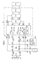
- the telecommunicaiton circuit shown in Fig. 1 includes a line circuit LC which is connected in cascade with a switch circuit HVC between a telecommunication line with conductors LI0 and LI1, connected to a subset TSS, and a switching network SNW.
- LC, HVC and SNW are located in a telecommunication exchange.
- Line circuit LC includes the cascade connection of a SLIC, a Digital Signal Processor DSP, a TransCoder and Filter circuit TCF and a Dual Processor Terminal Controller DPTC.
- Subset TSS includes a normally open hook switch HS connected between the line conductors L10 and L11.
- Switch circuit HVC is for instance of the type disclosed in Belgian patent No. 897 772. It includes 4 pairs of bidirecitonal switches sw00, sw01 to sw30, sw31 as shown and has line terminals L0 and L1 connected to line conductors LI0 and LI1 respectively, test terminals T0 and T1 connected to a test circuit TC, ringing terminals RG0 and RG1 connected to a ringing circuit RC, tip and ring terminals TP and RG connected to the like named outputs of line amplifiers LOA0 and LOA1 in the SLIC respectively and terminals STA, STB, SRA, SRB connected to like named terminals of a sensing circuit SENC in the SLIC.
- the line terminals L0/L1 are connected to TP/RG via the series connection of sw00/01, 50 ohms line feed resistors R0/1 and sw10/11 respectively.
- the respective junction points STB and SRA of sw00 and R0 and of sw01 and R1 are connected to TC via sw20 and sw21 respectively, whilst the respective junction points STA and SRB of R0 and sw10 and of R1 and sw11 are connected to RC via sw30 and sw31 respectively.
- series switches sw00, sw01, sw10 and sw11 are closed, whereas the other shunt switches are open.
- All the switches are controlled by the SLIC so that HVC is able to establish either one of the following connections : between TSS and SLIC (LOA0, LOA1 and SENC); TC and TSS; SLIC (LOA0, LOA1 and TC; RC and TSS; RC and SLIC (SENC).
- the function of TC is to test the connection to TSS and to the SLIC and that of RC is to apply a ringing signal to this line and to SENC in the SLIC.
- RC is able to connect ground through sw30 and the negative battery BA of -48 or -60 Volts in series with a ringing source RS of 90 Volts RMS through sw31.
- the Subscriber Line Interface Circuit SLIC which is integrated on a chip is a two-wire bidirectional circuit on the side of TSS and a four-wire one towards SNW. It has a speech receive input terminal Rx (with ground return) and a speech transmit output Tx (again with ground return), Rx and Tx being connected to DSP.
- the SLIC further has a 12 kHz or 16 kHz metering signal input terminal MTCF connected to TCF, data input and output terminals DSP1 and DSP2 connected to DSP and the above mentioned terminals STA, STB, SRA, SRB, TP and RG connected to HVC.
- the sensing circuit SENC included in the SLIC is of the type disclosed in European patent application No.
- i the line current comprising a DC component and possibly an AC component constituted by a speech signal and/or a metering signal.
- the digital signal processor DSP converts a digital speech signal received from TCF into an analog speech signal which is then applied to the speech receive terminal Rx of the SLIC. Conversely it converts an analog speech signal received via the speech transmit terminal Tx of the SLIC into a digital version which is applied to TCF.
- DSP also includes an echo canceller circuit.
- the DSP also receives on its data input terminal DSP2 control data bits transmitted by the SLIC. These bits are the same as those transmitted to DSP1 except that the four bits FR, RNG, CT0 and CT1 are respectively replaced by :
- the TCF performs a transcoding operation on digital signals received from the DSP and the DPTC and is also adapted to supply a metering signal MTCF to the SLIC. These operations are described in the Belgian patents 897 771 and 897 773.
- the DPTC performs the general control of the SLIC. Details of this circuit are described in the Belgian patents 898 959 and 898 960.
- circuits TCF and DSP are provided in common for a number of such lines, e.g. 8 lines, as indicated by the multipling arrows.
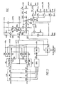
- Figs. 2 and 3 representing the polarity reversal circuit of Fig. 1 in more detail. This circuit operates with the following voltages :
- the output CO1 of the sensing circuit SENC is connected to the inputs VEET of both LOA0 and LOA1, which have respective feedback resistances R2 and R3, through a DC feedback circuit DCFC which together with the amplifiers LOA0 and LOA1, the feed resistances R0 and R1 and the sensing circuit SENC constitutes a resistance synthesis circuit, i.e. a circuit to convert the value of each of the feed resistances R0 and R1 into a wanted resistance value.
- the output CO1 of the sensing circuit SENC is also connected via a DC blocking capacitor C1 in series with an amplifier stage OA3 including an operational amplifier, on the one hand to the inverting input INO of LOA0 via resistance R4 and, on the other hand, to the non-inverting input NI1 of LOA1 through resistance R5 equal to R4.
- the amplifiers LOA0 and LOA1, the resistances R0 and R1, the sensing circuit SENC, the amplifier stage OA3 and the resistances R4 and R5 constitute an AC impedance synthesis circuit able to convert the resistance value of R0 and R1 into a wanted AC impedance.
- the non-inverting inputs NI0 of LOA0 and NI1 of LOA1 are connected through equal resistances R6 and R7 to the respective outputs VTI and VRI of a polarity reversal circuit PRC which as will be described later is able to apply a DC supply voltage V+ minus x to VTI and a DC voltage VEET plus x to VRI or vice-versa or even VEET plus x to both VTI and VRI.
- the voltage x is chosen in function of the magnitude of the speech signal and the metering signal and/or of one or more of the drive bits SMPI, HB, BPW.
- the PRC also provides at its output VX a voltage equal to V+ minus 2x which is applied to the DC feedback circuit DCFC.
- the non-inverting input NI0 of LOA0 and the inverting input IN1 of LOA1 are connected to VAG through respective equal bias resistances R8 and R9.
- the above mentioned outputs MTCF of TCF and Rx of DSP are coupled to the inverting input IN0 of LOA0 and to the non-inverting input NI1 of LOA1 via not shown means (indicating by dashed lines) and respective resistances R10, R11 and R12, R13.
- R10 and R12 are equal to R11 and R13 respectively.
- the output of the amplifier stage OA3 is also coupled via not shown means (also indicted by a dashed line) to the transmit output Tx.
- the not shown means are without importance for understanding the invention and are for instance of the type disclosed in the above mentioned European patent application.
- the polarity reversal circuit PRC includes a bias generation circuit BGC (Fig. 2) and a polarity reversal circuit proper PR (Fig. 3). It generates at its output VX a voltage equal to V+ - 2x and is adapted to apply voltages V+ - x and VEET + x to VTI and VRI respectively or to VRI and VTI respectively or to apply the voltage VEET + x to both VTI and VRI.
- the bias generation circuit BGC includes an operational amplifier OA2 to the non-inverting input of which the following bias voltages are able to be selectively connected :
- the voltages MBV, HBV and SBV are connected to the non-inverting input of amplifier OA2 via respective ones of the individual PNOS transistors PM1, PM2 and PM3 and a common PMOS transistor PM4, whereas the voltage RBV is connected to this input through PMOS transistor PM5.
- the transistors PM1, PM2, PM3, PM4 and PM5 are controlled by drive bit SMPI , Boolean function SMPI + HB , Boolean function SMPI + HB, drive bit BPW and drive bit BPW respectively.
- the selected one of the bias voltages MBV, HBV, SBV and RBV produces a corresponding value of the above mentioned voltage x. Because these bias voltages are derived from the low voltage B2 having a value equal to 2.41 Volts above VAG or from MBV having a value situated between VAUX and VAG respectively, the various transistors used may be of the low voltage type. Such transistors have the advantage of occupying a relatively small surface on the chip.
- the bias voltage is transformed first into a current and then again in a voltage in the following circuit.
- the output of amplifier OA2 is connected to its inverting input via the Darlington pair comprising NPN transistors N1 and N2 and bias resistance R19.
- the emitter of transistor N1 and the base of transistor N2 are joined and connected to the emitter of the latter transistor N2 through resistance R19.
- the junction point of N2 and R19 is connected to VAG via resistance R20, whilst V+ is connected to the joined collectors of N1 and N2 through resistances R21 and R22 in series.
- junction point JP1 of resistances R21 and R22 is connected to the base of PNP transistor P1 which together with NPN transistor N3 forms a common emitter - common collector pair.
- the supply voltage V+ is connected through resistance R23 to the command emitter of P1, collector of N3 and base of NPN transistor N4 whose collector is connected to V+.
- the collector of P1 is connected to the bases of NPN transistors N3 and N5 and the emitter of N3 is connected to input VEET via the series connection of diode connected NPN transistor N6 and resistances R24 and R25.
- the junction point of N6 and R24 is designated JP2 and the junction point of R24 and R25 is connected to VAG via capacitance C2 which forms together with resistances R24 and R25 another filter circuit.
- the emitters of transistors N4 and N5 constitute the outputs VHI and VLO of the circuit BGC respectively.
- This circuit further includes NPN transistors N7 and N8 whose emitters are connected to V-via resistances R27 and R28 respectively.
- the collector of N8 is connected to the junction point of the emitter of N4 and output VHI and the collector of N7 is connected to the junction point of transistors N18 and N ⁇ 18 in the circuit PR.
- Transistor N8 is a current mirror transistor coupled to a continuously operated current source - to be considered later - so that a constant current flows in its collector.
- Its base which constituted an input CUR of BGC is connected to the base of transistor N7 via the series connected NMOS transistors NM1 and NM2 the gates of which are controlled by the drive bits BR0 and BR1 respectively.
- the base of transistor N7 is also connected to V- via NMOS transistors NM3 and NM4 which are controlled by the bits BR0 and BR1 respectively.
- VBE of a transistor say N or P
- VHI V+ - x + V(P1) - V(N4)
- VLO VEET + (R24 + R25) I1 +V(N6) + V(N3) - V(N5)
- bits BRO and BR1 are both equal to 1, i.e. in the ground signalling condition, the base of transistor N8 is connected to that of transistor N7 through transistors NM1 and NM2 which are then both conductive. As a consquence current then flows from the junction point N18 and N ⁇ 18 in PR to V- via transistor N7 and resistance R27 in series. The reason for this will be explained later.
- the polarity reversal circuit proper PR includes a continuously operated current source comprising PMOS transistor PM6 controlled by constant voltage B1, NPN transistors N9 and N10 and resistance R29. More particularly, the supply voltage VAUX is connected to V-via the source-to-drain path of PM6, the collector-to-emitter path of N10 and resistance R29 in series. The collector and base of N10 are interconnected via the base-to-emitter junction of transistor N9 whose collector is connected to VAUX. The base of constant current source transistor N10 is connected to the base of current mirror NPN transistor N11 and V+ is connected to V- via resistance R30, the emitter-to-collector paths of PNP transistor P2 and NPN transistor N11, and resistance R31 in series.
- the base and collector of P2 are interconnected via the emitter-to-base junction of PNP transistor P3 whose collector is connected to V-.
- the constant current, say I2 produced is mirrored in the collector of transistor N8 of BGC and in first and second parts of PRC.
- the latter circuit parts are similar and differ only in the fact that the first (right hand part of Fig. 3) is controlled by drive bit BR0 and the complement thereof, whereas the second (left hand part of Fig. 3) is controlled by drive bits BR0 and BR1 and the complement thereof. Only the first circuit is considered hereinafter.
- the emitters of transistors N11 to N14 are connected to V- via respective resistances R31 to R34.
- a constant current is also mirrored in the collectors of PNP transistor P2, P4 and P5.
- the transistors N8, N11, N13, N14, P2, P4, P5 and their associated circuitry are so dimensioned that the currents flowing therein are equal to : I2 3 for N8; for N11, N13, P2, P4, P5; for N12; and for N14.
- I2 30 micro-Amperes.
- the supply voltage V+ is connected to V- through the series connection of resistance R35, the emitter-to-collector path of transistor P4, the collector-to-emitter path of diode connected NPN transistor N17 and, on the one hand resistance R36 in series with the emitter-to-collecter path of PNP transistor P6 and, on the other hand, the emitter-to-collector path of PNP transistor P7.
- the base of P6 is directly controlled from the output VHI of BGC and the junction point of the collectors of transistors P4 and N17 is connected to the output VTI of the circuit PR through the base-to-emitter junctions of NPN transistors N15 and N16.
- V+ is connected to the collectors of these transistors and the joined emitter of N15 and base of N16 are interconnected via bias resistance R37.
- N15, N16, R37 form a Darlington pair.
- the supply voltage V+ is also connected to the collector of transistor N14 via the series connection of resistance R38 and the emitter-to-collector path of transistor P5.
- the junction point of the collectors of transistors P5 and N14 is connected to the base of NPN transistor N18 whose emitter is connected to the output VLO of BGC via resistance R26 as well as to its base through resistance R39.
- V+ is connected to the junction point of the collector of transistor N18 and the base of transistor P7 via a current source/current mirror arrangement comprising diode connected transistor P8, PNP transistor P9 and resistances R40, R41 and R42, the collector and base of P8 being joined to the collector of transistor N13.
- the above mentioned second circuit part of the polarity reversal circuit proper PR differs from the just described first part in that the bases of transistors N ⁇ 12 and N ⁇ 13 are interconnected via the series connection of NMOS transistors NM ⁇ 5 and NM ⁇ 7 and that the interconnected bases of transistor N ⁇ 13 and N ⁇ 14 are connected to V- via NMOS transistors NM ⁇ 6 and NM ⁇ 8 in parallel.
- Transistors NM ⁇ 5, NM ⁇ 6, NM ⁇ 7 and NM ⁇ 8 are controlled by drive bits BRO, BR0 , BR1 and BR1 respectively.
- each of the above described first and second circuit parts of PR may be considered as including a gating means P6, P7; P ⁇ 6, P ⁇ 7, whose inputs are controlled from VHI directly and from VLO indirectly through transistors switch N18; N ⁇ 18 which is itself controlled from current source P5 and transistor switch N14.
- P7, P ⁇ 7 is also controlled from current source P9, P ⁇ 9 which is itself controlled from transistor switch N13, N ⁇ 13.
- transistors NM5 and NM ⁇ 6 are conductive, whereas transistors NM6 and NM ⁇ 5 are blocked so that the bases of transistor switches N8, N10, N11, N12, N ⁇ 12 are connected to those of transistor switch N13 and N14 which are then no longer inhibited, whereas transistors N ⁇ 13 and N ⁇ 14 are prevented from being operated and therefore block transistors P ⁇ 8 and P ⁇ 9.
- transistor N14 is conductive the current 2I2/3 provided by conductive transistor P5 is derived from the base of transistor N18 which is therefore prevented from being operated.
- transistor P7 of the gating means P6, P7 becomes conductive due to the voltage VHI being applied to its base.
- current mirror transistor P9 is conductive it charges all spurious capacitances of transistors P7 which will thus be able to be rapidly rendered conductive in case of a polarity reversal wherein a voltage VEET + x has to be applied to output VTI.
- transistor N ⁇ 14 is not conductive it derives no current, provided by transistor P ⁇ 5, from the base of transistor N ⁇ 18. As a consequence the latter transistor N ⁇ 18 is saturated by this the current so that the voltage VLO which is applied to the emitter of transistor N ⁇ 18 substantially appears at the collector thereof.
- transistor N13 is conductive.
- transistors P8 and P9 are conductive and because transistor N18 is blocked the current generated by transistor P9 is fed to the base of transistor P7.
- transistor P7 was previously conductive (in the reversal condition where the voltage VTI is then equal to VEET + x) it is now rapidly blocked so that the voltage VTI may rapidly become equal to V+ -x.
- the current source P9 is switched on by transistor N13 in case of a polarity reversal from the reversal condition to the normal condition. Otherwise, it remains switched off because transistor N13 is then blocked, as explained hereinafter.
- transistors NM5, NM ⁇ 6 and NM ⁇ 8 are blocked, whereas transistors NM6, NM ⁇ 5 and NM ⁇ 7 are conductive so that more particularly the base of transistor N ⁇ 12 is then connected to the bases of transistors N ⁇ 13 and N ⁇ 14 which are then no longer inhibited, whereas transistors N13 and N14 are prevented from being operated and therefore block transistors P8, P9 and N18.
- the above voltages V+ - x and VEET + x are supplied to the outputs VRI and VTI respectively.
- transistors NM5 and NM ⁇ 7 are blocked, whereas transistors NM6 and NM ⁇ 8 are conductive so that the bases of transistors N12 and N13 as well as of N ⁇ 12 and N ⁇ 13 are not interconnected.
- transistors NM1 and NM2 are conductive, whereas transistors NM3 and NM4 are blocked.
- transistor N7 is conductive, this transistor and associated circuitry being so determined that the current flowing through it is equal to Indeed, the current is constituted by constant current generated by transistor P5 and P ⁇ 5 and flowing through the base-to-emitter junctions of N18 (shunted by R39) and N ⁇ 18 (shunted by R ⁇ 39) respectively and which is now derived to V- via transitor N7 and resistance R27 in series and also by the current flowing from N5 to V- via R26, N7 and R27 in succession.
- transistors N18 and N ⁇ 18 are both saturated so that the voltage VLO - V(R26) is applied to the bases of transistors P7 and P ⁇ 7.
- the voltage VEET + x is then generated on both the outputs VTI and VRI.
- VHI the higher voltage VHI of the two voltages VHI and VLO is directly applied to transistor P6, whereas the lower voltage VLO - V(R26) is indirectly applied to P7 through transistor N18. This is done in order that the voltage in the commoned emitters of P6 and P7 (without considering R36) would be able to be made equal to VHI +(V(P6) or VLO - V(R26) + V(P7).
- VLO - V(R26) when VLO - V(R26) is not applied to P7 then the common emitter voltage is VHI + V(P6), whereas when VLO - V(R26) is applied to P7 then the commoned emitter voltage is VLO - (VR26) + V(P7) and P6 is blocked. If for instance VLO - V(R26) were directly applied to transistor P7 and VHI were indirectly applied to transistor P6 then it would be impossible to make the common emitter voltage equal to VHI + V(P6).
- the regulating resistances R36 and R ⁇ 36 are individually provided in the emitter branches of transistors P6 and P ⁇ 6 respectively, whereas the regulating resistance R26 is provided in common for transistors N18 and N ⁇ 18 associated to P7 and P ⁇ 7 respectively. This is done because the currents through the regulating resistances R26, R36, R ⁇ 36 are known and because R36 and R ⁇ 36 cannot be replaced by a single one since the current in the path leading from the output VHI of BGC to PR is not a constant.
- P6 and P7 instead of using PNP transistors for P6 and P7, it is also possible to make use of NPN transistors for P6 and P7, but in this case P6 has to be directly controlled from VLO whereas P7 has to be indirectly controlled from VHI. Also P9 has then to be so connected that it blocks P7 rapidly in case of a polarity reversal from the normal to reversal condition.
Landscapes
- Engineering & Computer Science (AREA)
- Computer Networks & Wireless Communication (AREA)
- Amplifiers (AREA)
- Monitoring And Testing Of Transmission In General (AREA)
- Devices For Supply Of Signal Current (AREA)
Claims (22)
- Polaritätsumkehrschaltung zur Umkehr der Polarität der Spannung zwischen einem ersten (LI0) und einem zweiten (LI1) Leiter einer Teilnehmeranschlußleitung, wobei diese Polaritätsumkehrschaltung eine Schaltung zur Erzeugnung einer Bezugsspannung mit mindestens einem Steuerausgang (JP1, JP2) enthält, der über elektronische Schalter zu mindestens einem Signalausgang (VTI, VRI) der Polaritätsumkehrschaltung führt und dieser Signalausgang mit der Teilnehmeranschlußleitung verbunden ist und Schaltungsanordnungen vorgesehen sind, um eine Bezugsspannung (V+ - x, VEET + x) mittels in Durchlaßrichtung betriebener Basis-Emitter-Strecken (P1, N4, P6, N17, N15, N16; N6, N3, N5, P7, N17, N15, N16) zu erzeugen,
dadurch gekennzeichnet,
daß die Bezugsspannung (V+ - x , VEET + x) an dem Steuerausgang (JP1, JP2) entsteht, der über eine Reihenschaltung aus in Durchlaßrichtung betriebener Basis-Emitter-Strecken (P1, N4, P6, N17, N15, N16; N6, N3, N5, P7, N17, N15, N16) bipolarer Transistoren und einem Kompensationswiderstand mit dem Signalausgang (VTI, VRI) verbunden ist, wobei ein definierter konstanter Strom durch den Kompensationswiderstand fließt und der Widerstandswert so gewählt wird, daß der Spannungsabfall über den Basis-Emitter-Strecken kompensiert wird, so daß an dem Signalausgang eine Spannung entsteht, die genau gleich der Bezugsspannung ist. - Polaritätsumkehrschaltung nach Anspruch 1, dadurch gekennzeichnet, daß sie Schaltungsanordnungen enthält, die einen konstanten Strom durch den Kompensationswiderstand (R26, R36) erzeugen.
- Polaritätsumkehrschaltung nach Anspruch 1, dadurch gekennzeichnet, daß die Schaltung zur Erzeugung einer Bezugsspannung einen ersten (JP1) und einen zweiten (JP2) Steuerausgang hat, an dem jeweils eine erste (V+ - x) und eine zweite (VEET + x) Bezugsspannung entsteht und der jeweils über eine erste Menge (P1, N4) und eine zweite Menge (N6, N3, N5) in Durchlaßrichtung betriebener Sperrschichten mit einem jeweils ersten (VHI) und einem zweiten (VLO) Anschluß verbunden ist, an denen jeweils Zwischenspannungen entstehen und die weiterverbunden werden mit einem ersten und einem zweiten Eingang der elektronischen Schalter, deren Ausgänge Signalausgänge (VTI, VRI) der Polaritätsumkehrschaltung sind, und daß der erste und zweite Eingang der elektronischen Schalter mit den Signalausgängen (VTI, VRI) der Polaritätsumkehrschaltung über eine dritte Menge (P6, N17, N15, N16) und eine vierte Menge (P7, N17, N15, N16) in Durchlaßrichtung betriebener Sperrschichten verbunden ist.
- Polaritätsumkehrschaltung nach Anspruch 3, dadurch gekennzeichnet, daß sie erste (P6, P7) und zweite (P'6, P'7) elektronische Schalter mit einem ersten (VTI) und einem zweiten (VRI) Signalausgang enthält, die mit dem jeweiligen ersten (LI0) und zweiten (LI1) Leiter der Teilnehmeranschlußleitung verbunden sind.
- Polaritätsumkehrschaltung nach Anspruch 3, dadurch gekennzeichnet, daß der elektronische Schalter einen ersten (P6) und einen zweiten (P7) Transistor enthält, deren Basisanschlüsse jeweils einen ersten und einen zweiten Eingang bilden und deren in Reihe mit dem jeweils gemeinsamen Teil (N17, N15, N16) der dritten (P6, N17, N15, N16) und der vierten (P7, N17, N15, N16) Menge der in Durchlaßrichtung betriebenen Sperrschichten geschalteten Emitter-Kollektor-Strecken zwischen einer Versorgungsspannung (v-) und dem Signalausgang (VTI, VRI) der Polaritätsumkehrschaltung liegen.
- Polaritätsumkehrschaltung nach Anspruch 5, dadurch gekennzeichnet, daß der erste (VHI) Anschluß, an dem eine Zwischenspannung entsteht, direkt mit dem ersten Eingang des elektronischen Schalters verbunden ist und daß der zweite (VLO) Anschluß, an dem eine Zwischenspannung entsteht, über einen ersten Transistorschalter (N18) mit dem zweiten Eingang des elektronischen Schalters verbunden ist, so daß bei leitendem erstem Transistorschalter (N18) der erste Transistor (P6) des elektronischen Schalters gesperrt und der zweite Transistor (P7) des elektronischen Schalters leitend (VLO) ist und dadurch die zweite Zwischenspannung an den Signalausgang (VTI, VRI) durchgeschaltet wird und daß bei gesperrtem ersten Transistorschalter (N18) der erste Transistor (P6) des elektronischen Schalters leitend ist und dadurch die erste Zwischenspannung (VHI) an den Signalausgang durchgeschaltet wird.
- Polaritätsumkehrschaltung nach Anspruch 6, dadurch gekennzeichnet, daß der erste Transistorschalter von einem dritten Transistor (N18) gebildet wird, dessen Kollektor-Emitter-Strecke zwischen dem zweiten Eingang des elektronischen Schalters und dem zweiten Ausgang (VLO), an dem eine Zwischenspannung entsteht, geschaltet ist und dessen Basis mit einer ersten Konstantstromquelle (P5) verbunden ist, und daß ein zweiter Transistorschalter (N14), wenn er durch die Steuerschaltung geöffnet wird, den dritten Transistor (N18) sperrt und dieser dann von der ersten Konstantstromquelle (P5) in die Sättigung getrieben wird und die zweite Zwischenspannung (VLO) somit an den zweiten Eingang des elektronischen Schalters gelangt.
- Polaritätsumkehrschaltung nach Anspruch 7, dadurch gekennzeichnet, daß Emitter und Basis des dritten Transistors (N18) über einen Widerstand (R39) miteinander verbunden sind.
- Polaritätsumkehrschaltung nach Anspruch 7, dadurch gekennzeichnet, daß der zweite Transistorschalter von einer geregelten zweiten Stromquelle (N14) gebildet wird.
- Polaritätsumkehrschaltung nach den Ansprüchen 2 und 5, dadurch gekennzeichnet, daß ein erster Kompensationswiderstand (R36) mit einer aus der dritten Menge in Durchlaßrichtung betriebener Diodenstrecken in Reihe geschaltet ist, wobei der Kompensationswiderstand (R36) von einem konstanten Strom aus einer dritten Konstantstromquelle (P4) durchflossen wird, die die Schaltung zur Erzeugung eines konstanten Stroms bildet.
- Polaritätsumkehrschaltung nach Anspruch 10, dadurch gekennzeichnet, daß die dritte Konstantstromquelle (P4) über einen als Diode geschalteten Transistor (N17) mit der jeweiligen Emitter-Kollektor-Strecke des ersten (P6) und zweiten (P7) Transistors verbunden ist und daß die dritte Konstantstromquelle (P4) und der als Diode geschaltete Transistor (N17) über eine Darlington-Schaltung (N15, N16) an den Signalausgang (VTI) der Polaritätsumkehrschaltung geschaltet sind.
- Polaritätsumkehrschaltung nach Anspruch 7, dadurch gekennzeichnet, daß ein zweiter Kompensationswiderstand (R26) in Reihe mit der Kollektor-Emitter-Strecke des dritten Transistors (N18) geschaltet ist.
- Polaritätsumkehrschaltung nach den Ansprüchen 4 und 12, dadurch gekennzeichnet, daß der zweite Kompensationswiderstand (R26) sowohl zum ersten (P6, P7) als auch zum zweiten (P'6, P'7) elektronischen Schalter gehört.
- Polaritätsumkehrschaltung nach Anspruch 7, dadurch gekennzeichnet, daß die Basis des zweiten Transistors (P7) mit einer vierten Konstantstromquelle (P9) verbunden ist und daß ein dritter Transistorschalter (N13), der gemeinsam mit dem zweiten Transistorschalter (N14) durch die Steuerschaltung geöffnet und geschlossen wird, wenn eine erste festgelegte Leitungsbedingung (Umpolung) hergestellt werden soll.
- Polaritätsumkehrschaltung nach Anspruch 1, dadurch gekennzeichnet, daß die Schaltung zur Erzeugung einer Bezugsspannung einen Spannungsteiler (R20, R21, R22) enthält, der mit einer Auswahlschaltung für unterschiedliche Vorspannungen (OA2) verbunden ist, die einen bestimmten Stromfluß durch den Spannungsteiler (R20, R21, R22) sichert, daß zu einem zweiten Widerstand (R21) des Spannungsteilers eine Reihenschaltung aus einem dritten Widerstand (R23) und der Emitter-Basis-Strecke eines vierten Transistors (P1) parallel geschaltet ist, wobei an die Basis des vierten Transistors (P1) die erste Bezugsspannung (V+ - x) angelegt wird und daß der Verbindungspunkt zwischem zweitem Widerstand (R21) und Emitter-Basis-Strecke des vierten Transistors (P1) über die Basis-Emitter-Strecke eines fünften Transistors (N4) an den zweiten Anschluß (VLO), an dem eine Zwischenspannung entsteht, geschaltet ist und die Kollektor-Emitter-Strecke des fünften Transistors (N4) über einen vierten Transistorschalter (N8) mit einer Versorgungsspannung (V-) verbunden ist, wobei der vierte Transistorschalter (N8) durch die Steuerschaltung ständig geöffnet wird.
- Polaritätsumkehrschaltung nach den Ansprüchen 4 und 15, dadurch gekennzeichnet, daß der Verbindungspunkt der Kollektor-Emitter-Strecken der zum ersten beziehungsweise zum zweiten elektronischen Schalter gehörenden dritten Transistoren (N18, N' 18) über einen fünften Transistorschalter (N7) mit einer Versorgungsspannung (V-) verbunden ist und der fünfte Transistorschalter (N7) zusammen mit dem vierten Transistorschalter (N8) durch die Steuerschaltung angesteuert wird, wenn eine zweite festgelegte Leitungsbedingung (Grundzustand) hergestellt werden soll.
- Polaritätsumkehrschaltung nach Anspruch 15, dadurch gekennzeichnet, daß der Verbindungspunkt zwischen zweitem Widerstand (R21) und Emitter-Basis-Strecke des vierten Transistors (P1) über die Kollektor-Emitter-Strecke eines sechsten Transistors (N3) und einem vierten Widerstand (R24 + R25), der den gleichen Widerstandswert wie der dritte Widerstand (R23) hat, mit einer dritten Bezugsspannung (VEET) verbunden ist und daß der sechste Transistor (N3) mit dem vierten Transistor (P1) eine Schaltungsanordnung bildet, die sicherstellt, daß durch den vierten Widerstand (R24 + R25) im wesentlichen der gleiche Strom fließt wie in dem zweiten Widerstand und daß die Basis des sechsten Transistors (N3) über die Basis-Emitter-Strecke eines siebenten Transistors (N5) mit dem zweiten Anschlußpunkt (VLO), an dem eine Zwischenspannung entsteht, verbunden ist.
- Polaritätsumkehrschaltung nach Anspruch 17, dadurch gekennzeichnet, daß die Basis-Emitter-Strecke des sechsten Transistors (N3) über die Basis-Emitter-Strecke eines zweiten als Diode geschalteten Transistors (N6) mit dem vierten Widerstand (R24 + R25) verbunden ist.
- Polaritätsumkehrschaltung nach Anspruch 17, dadurch gekennzeichnet, daß der vierte Widerstand (R24 + R25) den Längszweig eines Filters bildet, dessen Querzweig an einem Abgriff des Widerstandes von einem ersten Kondensator gebildet wird.
- Polaritätsumkehrschaltung nach Anspruch 15, dadurch gekennzeichnet, daß der zweite Widerstand (R21) einen Teil eines Längszweiges eines zweiten Filters bildet, dessen Querzweig von einem zweiten Kondensator (C1) gebildet wird.
- Polaritätsumkehrshaltung nach Anspruch 15, dadurch gekennzeichnet, daß die Auswahlschaltung für unterschiedliche Vorspannungen einen Operationsverstärker (OA2) enthält, dessen nichtinvertierender Eingang mit einer aus einer Mehrzahl von Vorspannungen (MBV, HBV, SBV, RBV) ausgewählten Vorspannung verbunden werden kann und dessen Ausgangssignal eine Darlingtonschaltung (W1, W2) ansteuert, die in Reihe mit dem zweiten Widerstand (R21) und einem fünften Widerstand (R20) liegt.
- Polaritätsumkehrschaltung nach Anspruch 21, dadurch gekennzeichnet, daß die Vorspannungen kleiner als die Bezugsspannungen sind.
Applications Claiming Priority (2)
| Application Number | Priority Date | Filing Date | Title |
|---|---|---|---|
| BE2/60895A BE903911R (nl) | 1983-10-21 | 1985-12-20 | Telecommunicatielijnketen en bijbehorende polariteitsomkeerketen. |
| BE2060895 | 1985-12-20 |
Publications (3)
| Publication Number | Publication Date |
|---|---|
| EP0241604A2 EP0241604A2 (de) | 1987-10-21 |
| EP0241604A3 EP0241604A3 (en) | 1988-06-15 |
| EP0241604B1 true EP0241604B1 (de) | 1992-06-24 |
Family
ID=3865779
Family Applications (1)
| Application Number | Title | Priority Date | Filing Date |
|---|---|---|---|
| EP19860202326 Expired EP0241604B1 (de) | 1985-12-20 | 1986-12-18 | Polaritätsumkehrschaltung |
Country Status (3)
| Country | Link |
|---|---|
| EP (1) | EP0241604B1 (de) |
| AU (1) | AU590809B2 (de) |
| ES (1) | ES2004502A6 (de) |
Family Cites Families (2)
| Publication number | Priority date | Publication date | Assignee | Title |
|---|---|---|---|---|
| BE898051A (nl) * | 1983-10-21 | 1984-04-24 | Bell Telephone Mfg | Telecommunicatielijnketen en bijbehorende polariteitsomkeerketen. |
| AU5364886A (en) * | 1985-02-28 | 1986-09-04 | International Standard Electric Corp. | Polarity reversal circuit |
-
1986
- 1986-12-09 AU AU66338/86A patent/AU590809B2/en not_active Ceased
- 1986-12-18 EP EP19860202326 patent/EP0241604B1/de not_active Expired
- 1986-12-19 ES ES8603518A patent/ES2004502A6/es not_active Expired
Also Published As
| Publication number | Publication date |
|---|---|
| AU6633886A (en) | 1987-06-25 |
| EP0241604A2 (de) | 1987-10-21 |
| ES2004502A6 (es) | 1989-01-16 |
| AU590809B2 (en) | 1989-11-16 |
| EP0241604A3 (en) | 1988-06-15 |
Similar Documents
| Publication | Publication Date | Title |
|---|---|---|
| US4041252A (en) | Transformerless two-wire/four-wire hybrid with DC sourcing capability | |
| US5175764A (en) | Enhanced high voltage line interface circuit | |
| CA1202742A (en) | Loop-start/ground-start line interface circuit | |
| EP0201635B1 (de) | Fernmeldeleitungsschaltung | |
| EP0272800B1 (de) | Leitungsspeiseschaltung mit aktiver Impedanz | |
| GB1389560A (en) | Active two-wire to four-wire coupling circuit | |
| AU644162B2 (en) | Telecommunications line circuit | |
| US4139731A (en) | Telephone conference system with active analog conference | |
| US4322586A (en) | Transformerless line interface circuit | |
| EP0241604B1 (de) | Polaritätsumkehrschaltung | |
| EP0237656B1 (de) | Fernmeldeleitungsschaltung mit darin verwendeter Verstärkerschaltung | |
| CA1240088A (en) | Solid state trunk circuit | |
| CA1160780A (en) | Trunk interface circuit with current compensation | |
| US4358645A (en) | Loop sensing circuit for use with a subscriber loop interface circuit | |
| US4485341A (en) | Current limiter circuit | |
| GB2149618A (en) | Telecommunication line circuit and associated voltage converter | |
| EP0096473B1 (de) | Leitungsspeiseschaltung aktiver Impedanz | |
| CA1143493A (en) | Connecting circuit for a telephone line | |
| US3987254A (en) | Transformerless amplification circuitry for telecommunication system | |
| US4614840A (en) | Telecommunication line circuit and associated polarity reversal circuit | |
| US4267408A (en) | Arrangement for applying a signal to a transmission line | |
| US4742540A (en) | Circuit for switching between balanced networks | |
| BE903910R (nl) | Telecommunicatielijnketen en bijbehorende spanningsomzetter. | |
| BE903911R (nl) | Telecommunicatielijnketen en bijbehorende polariteitsomkeerketen. | |
| GB1034827A (en) | Telephone systems with conference call facility |
Legal Events
| Date | Code | Title | Description |
|---|---|---|---|
| PUAI | Public reference made under article 153(3) epc to a published international application that has entered the european phase |
Free format text: ORIGINAL CODE: 0009012 |
|
| AK | Designated contracting states |
Kind code of ref document: A2 Designated state(s): FR GB IT |
|
| RAP1 | Party data changed (applicant data changed or rights of an application transferred) |
Owner name: ALCATEL N.V. |
|
| RAP3 | Party data changed (applicant data changed or rights of an application transferred) |
Owner name: ALCATEL N.V. |
|
| PUAL | Search report despatched |
Free format text: ORIGINAL CODE: 0009013 |
|
| AK | Designated contracting states |
Kind code of ref document: A3 Designated state(s): FR GB IT |
|
| 17P | Request for examination filed |
Effective date: 19881207 |
|
| 17Q | First examination report despatched |
Effective date: 19910131 |
|
| GRAA | (expected) grant |
Free format text: ORIGINAL CODE: 0009210 |
|
| AK | Designated contracting states |
Kind code of ref document: B1 Designated state(s): FR GB IT |
|
| ET | Fr: translation filed | ||
| ITF | It: translation for a ep patent filed | ||
| PG25 | Lapsed in a contracting state [announced via postgrant information from national office to epo] |
Ref country code: GB Effective date: 19921218 |
|
| PLBE | No opposition filed within time limit |
Free format text: ORIGINAL CODE: 0009261 |
|
| STAA | Information on the status of an ep patent application or granted ep patent |
Free format text: STATUS: NO OPPOSITION FILED WITHIN TIME LIMIT |
|
| 26N | No opposition filed | ||
| GBPC | Gb: european patent ceased through non-payment of renewal fee |
Effective date: 19921218 |
|
| PGFP | Annual fee paid to national office [announced via postgrant information from national office to epo] |
Ref country code: FR Payment date: 20041213 Year of fee payment: 19 |
|
| PG25 | Lapsed in a contracting state [announced via postgrant information from national office to epo] |
Ref country code: IT Free format text: LAPSE BECAUSE OF NON-PAYMENT OF DUE FEES;WARNING: LAPSES OF ITALIAN PATENTS WITH EFFECTIVE DATE BEFORE 2007 MAY HAVE OCCURRED AT ANY TIME BEFORE 2007. THE CORRECT EFFECTIVE DATE MAY BE DIFFERENT FROM THE ONE RECORDED. Effective date: 20051218 |
|
| PG25 | Lapsed in a contracting state [announced via postgrant information from national office to epo] |
Ref country code: FR Free format text: LAPSE BECAUSE OF NON-PAYMENT OF DUE FEES Effective date: 20060831 |
|
| REG | Reference to a national code |
Ref country code: FR Ref legal event code: ST Effective date: 20060831 |