EP0240710B1 - Near-linear spring connect structure for flexible interconnect circuits - Google Patents
Near-linear spring connect structure for flexible interconnect circuits Download PDFInfo
- Publication number
- EP0240710B1 EP0240710B1 EP87102972A EP87102972A EP0240710B1 EP 0240710 B1 EP0240710 B1 EP 0240710B1 EP 87102972 A EP87102972 A EP 87102972A EP 87102972 A EP87102972 A EP 87102972A EP 0240710 B1 EP0240710 B1 EP 0240710B1
- Authority
- EP
- European Patent Office
- Prior art keywords
- cylinders
- contact
- force
- pads
- dimples
- Prior art date
- Legal status (The legal status is an assumption and is not a legal conclusion. Google has not performed a legal analysis and makes no representation as to the accuracy of the status listed.)
- Expired - Lifetime
Links
Images
Classifications
-
- H—ELECTRICITY
- H01—ELECTRIC ELEMENTS
- H01R—ELECTRICALLY-CONDUCTIVE CONNECTIONS; STRUCTURAL ASSOCIATIONS OF A PLURALITY OF MUTUALLY-INSULATED ELECTRICAL CONNECTING ELEMENTS; COUPLING DEVICES; CURRENT COLLECTORS
- H01R12/00—Structural associations of a plurality of mutually-insulated electrical connecting elements, specially adapted for printed circuits, e.g. printed circuit boards [PCB], flat or ribbon cables, or like generally planar structures, e.g. terminal strips, terminal blocks; Coupling devices specially adapted for printed circuits, flat or ribbon cables, or like generally planar structures; Terminals specially adapted for contact with, or insertion into, printed circuits, flat or ribbon cables, or like generally planar structures
- H01R12/70—Coupling devices
- H01R12/77—Coupling devices for flexible printed circuits, flat or ribbon cables or like structures
- H01R12/79—Coupling devices for flexible printed circuits, flat or ribbon cables or like structures connecting to rigid printed circuits or like structures
-
- H—ELECTRICITY
- H05—ELECTRIC TECHNIQUES NOT OTHERWISE PROVIDED FOR
- H05K—PRINTED CIRCUITS; CASINGS OR CONSTRUCTIONAL DETAILS OF ELECTRIC APPARATUS; MANUFACTURE OF ASSEMBLAGES OF ELECTRICAL COMPONENTS
- H05K3/00—Apparatus or processes for manufacturing printed circuits
- H05K3/36—Assembling printed circuits with other printed circuits
- H05K3/361—Assembling flexible printed circuits with other printed circuits
- H05K3/365—Assembling flexible printed circuits with other printed circuits by abutting, i.e. without alloying process
Definitions
- the invention relates to a near-linear spring connect structure and to a method of making forced, yet removable contact between an electronic substrate like a printhead and a flexible interconnect circuit in accordance with the precharacterizing parts of the claims 1 and 4, respectively.
- a spring connect structure of this type is known from Hewlett-Packard Journal, Vol. 36, No. 5, May, 1985, page 14; R.t. Buck: "Printhead interconnect”.
- heater resistors In the manufacture of thin film resistor substrates for thermal ink jet printheads, it is known to provide heater resistors on a common substrate, such as silicon, and employ these resistors to transfer thermal energy to corresponding adjacent ink reservoirs during a thermal ink jet printing operation. This thermal energy will cause the ink in the reservoirs to be heated to boiling and thereby be ejected through an orifice in an adjacent nozzle plate from which it is directed onto a print medium. During such operation, these heater resistors are electrically pulsed by current applied thereto via conductive traces formed on top of the silicon substrate and insulated therefrom by an intermediate dieletric layer.
- this layer the formation of this layer, the formation of the resistive layer for the heater resistors, and the aluminum evaporation or sputtering process for forming electrical patterns of conductive trace material to the heater resistors are all well known in the art and therefore are not described in further detail herein.
- the various processes used in the fabrication of thermal ink jet printheads reference may be made to the Hewlett Packard Journal , Volume 36, Number 5, May 1985.
- the flexible circuit will typically consist of a photolithographically defined conductive pattern which has been formed by metal evaporation or sputtering and etching processes carried out on a thin flexible insulating substrate member.
- These electrical contact locations on the flex circuit will be raised slightly in a bump and dimple configuration, and this geometry may be achieved by the use of a "bed of nails” punch structure which match the location of the dimples. This structure is used to punch the electrical contact locations on the flex circuit to a raised location above the surface of the insulating substrate member thereof.
- the tips of these cones can be inserted into the dimples of the flex circuit and urged thereagainst with a force sufficient to bring the conductive bumps on the flex circuit into good physical and electrical contact with the terminal pads on the thin film resistor substrate.
- this nonlinear characteristic tends to increase the amount of force which must be applied to the flex circuit in order to insure that all the bumps on the flex circuit make good electrical contact with the conductive traces or terminal pads on the printhead substrate. In some cases this required force is sufficiently large to fracture the substrate or do other structural damage thereto.
- This nonlinear deflection characteristic of the prior art according to Hewlett-Packard Journal is described in more detail below with reference to the prior art Fig. 1A and 1B.
- the object of this invention is to reduce the amount of force required to assure good electrical contact between a flexible circuit and a thin film resistor substrate for a thermal ink jet printhead.
- Dependant claims 2 and 3 characterize advantageous developments of the structure defined in claim 1.
- Dependant claim 5 characterizes an advantageous development of the method according to claim 4.
- cone-shaped tips are located at upper ends of the elastomeric deflectable cylinders and are inserted into dimples of the flexible circuit with a force sufficient to bring the electrical bumps or pads above the dimples into good electrical contact with mating conductive contact pads on the printhead substrate.
- the volumetric deformation of the cylinders varies substantially linearally as a function of the force applied to the lower ends of these cylinders, and this feature enables the vertical displacement of the cylinder walls to be maximized for a given force applied to these cylinders.
- the cylinders are hollow and are made of rubber or other like elastomeric material.
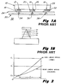
- Figures 1A and 1B illustrate the cone shaped spring interconnect structure of the prior art.
- Figure 2 is a graph illustrating the linear versus nonlinear variations in volumetric compression of the cylinder and cone configurations, respectively, as a function of the variation in distance of compression of these members.
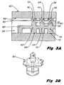
- Figure 3A is a schematic representation of the spring connect structure-flex circuit-printhead interconnect scheme of the present invention.
- Figure 3B is an enlarged isometric view of one of the cylindrical interconnects of Figure 3A.
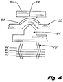
- Figure 4 is an enlarged cross section view of the compression and bulging of the cylindrical walls (exaggeratedly spaced) of the elastomeric cylinders of the spring connect structure of Figures 3A and 3B.
- FIG. 1A there is shown schematically a thin film resistor printhead substrate 10 which has been fabricated using state-of-the-art semiconductor processing technique and includes a plurality of electrically conductive pads 12, 14 and 16 thereon. It is desired to connect these pads 12, 14 and 16 to a corresponding plurality of flex pads 18, 20 and 22 on a flexible or "flex" circuit member 24.
- the flex circuit member 24 will typically consist of a thin flexible insulating member of a material such as Mylar upon which a conductive pattern has been deposited thereon and etched in a given geometry so that the conductive pads 18, 20 and 22 will be formed thereon at a desired spacing as shown.
- each succeeding volume V0, V1, V2 and V3 becomes increasingly larger. Furthermore, this increasing volumetric relationship varies geometrically and therefore leads to a very nonlinear spring as indicated by the curve in Figure 2.
- the load L1 increases rapidly with an increasing cone tip displacement or height variation, indicated as delta, ⁇ . This characteristic is undesirable because it leads to larger and heavier interconnect parts, and it sometimes produces creep in the substrate material and sometimes causes breakage or fracture of the thin film resistor substrate.
- a near linear spring provides a lower final load L1' which is sufficient to bring all contact pads on the flex circuit into contact with corresonding terminal contact pads on the thin film resistor substrate.
- a printhead 40 which may for example be a thin film resistor type printhead having contact pads 42, 44, and 46 on the lower surface thereof.
- a flexible circuit member 50 having a conductive pattern thereon has been brought into alignment with the substrate 40 as shown, with contact pads 52, 54 and 56 of the flex circuit pattern being aligned with the contact pads 42, 44, and 46 on the printhead 40, respectively.
- a near-linear spring connect structure is generally designated 58 and includes a horizontal central locating member 60 and a plurality of hollow rubber cylinders 62, 64 and 66 which extend therethrough as shown.
- the cylinders 62, 64 and 66 include lower cylindrical sections 68, 70 and 72 which extend downwardly and come to rest on a rigid base support member 76.
- the spring connect structure 58 further includes a plurality of upper, partially cylindrical and partially conical sections 78, 80 and 82 with conical tips which are brought into alignment with the underside of the dimples in the flex circuit 50. This partially cylindrical and partially conical (tip) configuration is better seen in the enlarged isometric view of Figure 3B wherein the cylindrical structure on the topside of the central locating member 60 is of solid construction and on the underside of member 60 is of hollow construction.
- a rubber cylinder such as cylinder 70 will undergo a slight bulge as indicated when forces are applied vertically to the spring connect structure 58 (Fig. 3) to urge the contact pad 54 of the flexible circuit 50 into electrical contact with the contact pad 44 on the printhead 40.
- the walls of the cylinder 70 bulge slightly as indicated, the successive volume displacements are not exactly equal, and this reaction leads to a spring which is nearly linear, rather that precisely linear.
- this cylindrical shape is the most nearly linear spring which can be manufactured at a minimum cost and which yields the near linear load versus distance curve in Figure 2.
- This spring connect structure 58 is capable of bringing all pads 52, 54 and 56 into contact with all corresponding contact pads 42, 44 and 46 on the printhead 40 (Fig.3) after applying a minimum force of. approximately L1' shown in Figure 2, as contrasted to the much greater force L1 for the nonlinear spring of the prior art shown in Figures 1A and 1B.
- the cylindrical columns may be either solid or hollow.
- the present invention is not limited to the electrical connection of flexible circuits to ink jet printheads, but may be used for the connection of flex circuits to other equivalent small geometry electronic devices having small contact pads thereon to which removable pressure connections need be made.
- the present invention is used for the removable electrical connection of flexible interconnect circuits to thermal ink jet printheads or other small electronic devices requiring such removable connection. These printheads are used for controlling the ejection of ink from a thermal ink jet printer during a high speed printing operation.
Description
- The invention relates to a near-linear spring connect structure and to a method of making forced, yet removable contact between an electronic substrate like a printhead and a flexible interconnect circuit in accordance with the precharacterizing parts of the claims 1 and 4, respectively. A spring connect structure of this type is known from Hewlett-Packard Journal, Vol. 36, No. 5, May, 1985, page 14; R.t. Buck: "Printhead interconnect".
- In the manufacture of thin film resistor substrates for thermal ink jet printheads, it is known to provide heater resistors on a common substrate, such as silicon, and employ these resistors to transfer thermal energy to corresponding adjacent ink reservoirs during a thermal ink jet printing operation. This thermal energy will cause the ink in the reservoirs to be heated to boiling and thereby be ejected through an orifice in an adjacent nozzle plate from which it is directed onto a print medium. During such operation, these heater resistors are electrically pulsed by current applied thereto via conductive traces formed on top of the silicon substrate and insulated therefrom by an intermediate dieletric layer. The formation of this layer, the formation of the resistive layer for the heater resistors, and the aluminum evaporation or sputtering process for forming electrical patterns of conductive trace material to the heater resistors are all well known in the art and therefore are not described in further detail herein. However, for a further discussion of the various processes used in the fabrication of thermal ink jet printheads, reference may be made to the Hewlett Packard Journal,
Volume 36, Number 5, May 1985. - In order to provide electrical connections between external pulse drive circuits and these conductive traces on the thermal ink jet printhead, it has been a common practice to employ so called flexible or "flex" circuits to make removeable pressure contacts to certain conductive terminal pads on the thin film resistor printhead substrate. For this connection it becomes necessary to provide means by which pressure can be applied to the flexible circuit so that the electrical leads therein make good electrical connection with corresponding mating pads on the thin film resistor substrate.
- The flexible circuit will typically consist of a photolithographically defined conductive pattern which has been formed by metal evaporation or sputtering and etching processes carried out on a thin flexible insulating substrate member. These electrical contact locations on the flex circuit will be raised slightly in a bump and dimple configuration, and this geometry may be achieved by the use of a "bed of nails" punch structure which match the location of the dimples. This structure is used to punch the electrical contact locations on the flex circuit to a raised location above the surface of the insulating substrate member thereof.
- During this latter punch process, it sometimes happens that not all of the raised contact bumps in the flexible circuit are moved the same distance above the insulating substrate surface. For this reason, more force is necessary to make contact with the smaller or lower-height bumps than those higher bumps more extended from the surface of the flex circuit The known printhead interconnection according to Hewlett-Packard Journal provides the necessary force to the flex circuit and the necessary pressure contact between the flex circuit and conductive pads on the thin film resistor substrate by using an elastomeric material, such as rubber, which has been preformed to have a plurality of cones spaced at locations corresponding to the location of the dimples in the flex circuit. In this manner, the tips of these cones can be inserted into the dimples of the flex circuit and urged thereagainst with a force sufficient to bring the conductive bumps on the flex circuit into good physical and electrical contact with the terminal pads on the thin film resistor substrate.
- While the above prior art approach to making electrical contact between the flex circuit and the printhead substrate has proven satisfactory for certain types of interconnect patterns with few interconnect members, it has not been entirely satisfactory for connecting larger numbers of conductive traces to larger numbers of conductive bumps or pads on the flex circuit. This fact has been a result of the nature of the nonlinear deflection of the above elastomeric cones. This nonlinear deflection of the elastomeric cones is seen as a nonlinear variation in cone volumetric compression, VC' as a function of the distance, D, that the tip of the cone is moved during an interconnect operation. Thus, this nonlinear characteristic tends to increase the amount of force which must be applied to the flex circuit in order to insure that all the bumps on the flex circuit make good electrical contact with the conductive traces or terminal pads on the printhead substrate. In some cases this required force is sufficiently large to fracture the substrate or do other structural damage thereto. This nonlinear deflection characteristic of the prior art according to Hewlett-Packard Journal is described in more detail below with reference to the prior art Fig. 1A and 1B.
- The object of this invention is to reduce the amount of force required to assure good electrical contact between a flexible circuit and a thin film resistor substrate for a thermal ink jet printhead.
- This object is, according to the invention solved by a near-linear spring connect structure and a method according to the features specified in the independent claims 1 and 4, respectively.
- Dependant claims 2 and 3 characterize advantageous developments of the structure defined in claim 1. Dependant claim 5 characterizes an advantageous development of the method according to claim 4.
- In a preferred embodiment of the invention, cone-shaped tips are located at upper ends of the elastomeric deflectable cylinders and are inserted into dimples of the flexible circuit with a force sufficient to bring the electrical bumps or pads above the dimples into good electrical contact with mating conductive contact pads on the printhead substrate. During this process, the volumetric deformation of the cylinders varies substantially linearally as a function of the force applied to the lower ends of these cylinders, and this feature enables the vertical displacement of the cylinder walls to be maximized for a given force applied to these cylinders. In a preferred embodiment, the cylinders are hollow and are made of rubber or other like elastomeric material.
- Figures 1A and 1B illustrate the cone shaped spring interconnect structure of the prior art.
- Figure 2 is a graph illustrating the linear versus nonlinear variations in volumetric compression of the cylinder and cone configurations, respectively, as a function of the variation in distance of compression of these members.
- Figure 3A is a schematic representation of the spring connect structure-flex circuit-printhead interconnect scheme of the present invention.
- Figure 3B is an enlarged isometric view of one of the cylindrical interconnects of Figure 3A.
- Figure 4 is an enlarged cross section view of the compression and bulging of the cylindrical walls (exaggeratedly spaced) of the elastomeric cylinders of the spring connect structure of Figures 3A and 3B.
- Referring now to Figure 1A, there is shown schematically a thin film
resistor printhead substrate 10 which has been fabricated using state-of-the-art semiconductor processing technique and includes a plurality of electricallyconductive pads pads flex pads circuit member 24. Theflex circuit member 24 will typically consist of a thin flexible insulating member of a material such as Mylar upon which a conductive pattern has been deposited thereon and etched in a given geometry so that theconductive pads - As previously mentioned, during the creation of the contour of the
conductive pads flex circuit 24, using a bed-of-nails punch-type of press or the like, it frequently happens that while onepad 18 may be pressed upwardly to a desired height,other pads 20 and 22 will not be so raised. Thus,gaps pads 20 and 22 and the surfaces of theconductive pads 14 and 16 prior to being forced further upwardly by an additional force applied to thebase 30 of the non-linear cone-typeinterconnect spring structure 32 of the prior art. Thisstructure 32 will typically have a plurality ofelastomeric cones cones prior art struture 32 have typically been molded of rubber and are of solid construction. - As indicated in Figure 1B, as each
cone - Referring now to Figure 3A, there is shown a
printhead 40, which may for example be a thin film resistor type printhead havingcontact pads flexible circuit member 50 having a conductive pattern thereon has been brought into alignment with thesubstrate 40 as shown, withcontact pads contact pads printhead 40, respectively. - A near-linear spring connect structure is generally designated 58 and includes a horizontal central locating
member 60 and a plurality ofhollow rubber cylinders cylinders cylindrical sections spring connect structure 58 further includes a plurality of upper, partially cylindrical and partiallyconical sections 78, 80 and 82 with conical tips which are brought into alignment with the underside of the dimples in theflex circuit 50. This partially cylindrical and partially conical (tip) configuration is better seen in the enlarged isometric view of Figure 3B wherein the cylindrical structure on the topside of the central locatingmember 60 is of solid construction and on the underside ofmember 60 is of hollow construction. - Referring now to Figure 4, a rubber cylinder such as
cylinder 70 will undergo a slight bulge as indicated when forces are applied vertically to the spring connect structure 58 (Fig. 3) to urge thecontact pad 54 of theflexible circuit 50 into electrical contact with thecontact pad 44 on theprinthead 40. Ideally, each successive displaced volulme equals the last, i. e. V₀' = V₁' = V₂' = V₃'. However, because the walls of thecylinder 70 bulge slightly as indicated, the successive volume displacements are not exactly equal, and this reaction leads to a spring which is nearly linear, rather that precisely linear. However, this cylindrical shape is the most nearly linear spring which can be manufactured at a minimum cost and which yields the near linear load versus distance curve in Figure 2. Thisspring connect structure 58 is capable of bringing allpads corresponding contact pads - The cylindrical columns may be either solid or hollow. In addition, the present invention is not limited to the electrical connection of flexible circuits to ink jet printheads, but may be used for the connection of flex circuits to other equivalent small geometry electronic devices having small contact pads thereon to which removable pressure connections need be made.
- The present invention is used for the removable electrical connection of flexible interconnect circuits to thermal ink jet printheads or other small electronic devices requiring such removable connection. These printheads are used for controlling the ejection of ink from a thermal ink jet printer during a high speed printing operation.
Claims (5)
- A spring connect structure (58) comprising:A plurality of resilient members (62, 64, 66), said members (62, 64, 66) spaced laterally apart by predetermined distances corresponding to predetermined dimensions on a flexible interconnect circuit (50) at which electrical contact areas (52, 54, 56) are located, whereby tips of said members (62, 64, 66) are adapted to be brought into forcible contact with said interconnect circuit (50) to urge said interconnect circuit into electrical contact with another electronic structure (42, 44, 46) aligned therewith,characterized in that said members (62, 64, 66) comprise resilient cylinders, and a horizontal central locating member (60) is provided for carrying said plurality of resilient cylinders (62, 64, 66) so that they extend integrally therethrough or therefrom a predetermined distance from the major surfaces of said central locating member (60),and the volume displacement within said cylinders (62, 64, 66) as a result of force being applied thereto is nearly linear with respect to said force and thereby enables the vertical displacement of said cylinders (62, 64, 66) to be maximized for a given force applied thereto, thereby minimizing the required force applied to said electronic structure.
- The spring connect structure defined in claim 1, characterized in that said cylinders (62, 64, 66) are made of rubber and have either a hollow volume or a solid volume bounded by cylindrical walls extending normal to a major surface of said central locating member (60).
- The spring connect structure as defined in claim 1 or 2, characterized in that said tips of said cylinders are cone shaped and located at upper ends of said cylinders and are inserted into dimples of said flexible interconnect circuit (50) with a force sufficient to bring the electrical contact areas above said dimples into good electrical contact with contact pads of said another electronic structure.
- A method of making forced, yet removable contact between an electronic substrate (40) in particular a printhead having a plurality of contact pads (42, 44, 46) thereon and a flexible interconnect circuit (50) having a corresponding plurality of contact pads (52, 54, 56) and dimples thereon which comprises the steps of:a) aligning said plurality of contact pads (52, 54, 56) and dimples on said flexible circuit (50) with a matching plurality of said contact pads (42, 44, 46) on said electronic substrate (40), andb) urging the ends of a mating plurality of members (62, 64, 66) being laterally spaced at distances corresponding to the spacings between the pads and dimples on said flexible interconnect circuit (50),characterized by using elastomeric cylinders for said members (62, 64, 66) such that the volume displacement of said elastomeric cylinders (62, 64, 66) as a result of force applied thereto is nearly linear and thereby enables the vertical displacement of said cylinders (62, 64, 66) to be maximized for a given applied force and tends to minimize the amount of force required to drive all mating contact pads on said substrate and flexible circuit into electrical contact, and the lowering of such contact force enables the number and packing density of contact pads to be maximized.
- The method according to claim 4,further characterized byc) providing a central locating member wherein said plurality of elastomeric cylinders extends integrally and perpendicularly therefrom and is laterally spaced on said central locating member at said distances corresponding to the spacings between said pads and dimples on said flexible circuit (50).
Applications Claiming Priority (2)
| Application Number | Priority Date | Filing Date | Title |
|---|---|---|---|
| US848366 | 1986-04-03 | ||
| US06/848,366 US4706097A (en) | 1986-04-03 | 1986-04-03 | Near-linear spring connect structure for flexible interconnect circuits |
Publications (3)
| Publication Number | Publication Date |
|---|---|
| EP0240710A2 EP0240710A2 (en) | 1987-10-14 |
| EP0240710A3 EP0240710A3 (en) | 1990-02-07 |
| EP0240710B1 true EP0240710B1 (en) | 1996-02-07 |
Family
ID=25303067
Family Applications (1)
| Application Number | Title | Priority Date | Filing Date |
|---|---|---|---|
| EP87102972A Expired - Lifetime EP0240710B1 (en) | 1986-04-03 | 1987-03-03 | Near-linear spring connect structure for flexible interconnect circuits |
Country Status (5)
| Country | Link |
|---|---|
| US (1) | US4706097A (en) |
| EP (1) | EP0240710B1 (en) |
| JP (1) | JPH078571B2 (en) |
| CA (1) | CA1293783C (en) |
| DE (1) | DE3751695T2 (en) |
Families Citing this family (35)
| Publication number | Priority date | Publication date | Assignee | Title |
|---|---|---|---|---|
| USRE37671E1 (en) | 1987-10-23 | 2002-04-30 | Hewlett-Packard Company | Printhead-carriage alignment and electrical interconnect lock-in mechanism |
| JP2509656B2 (en) * | 1988-02-17 | 1996-06-26 | 住友電気工業株式会社 | Flexible printed wiring board connection structure |
| US4878070A (en) * | 1988-10-17 | 1989-10-31 | Xerox Corporation | Thermal ink jet print cartridge assembly |
| US5515086A (en) * | 1991-01-15 | 1996-05-07 | Canon Kabushiki Kaisha | Contact structure between flexible cable and signal receiving unit and recording apparatus using said contact structure |
| ATE177688T1 (en) * | 1992-07-30 | 1999-04-15 | Canon Kk | RECORDING HEAD AND RECORDING DEVICE USING SAME |
| DE69328714T2 (en) * | 1992-12-25 | 2000-12-28 | Canon Kk | Liquid jet head and device therefor |
| US5295839A (en) * | 1993-03-16 | 1994-03-22 | Hewlett-Packard Company | Method and system for interconnectingly engaging circuits |
| DE69405435T2 (en) * | 1993-03-16 | 1998-01-22 | Hewlett Packard Co | Method and device for the production of electrically interconnected circuits |
| EP0616394A1 (en) * | 1993-03-16 | 1994-09-21 | Hewlett-Packard Company | Method and system for producing electrically interconnected circuits |
| US5372512A (en) * | 1993-04-30 | 1994-12-13 | Hewlett-Packard Company | Electrical interconnect system for a flexible circuit |
| US5598194A (en) * | 1993-04-30 | 1997-01-28 | Hewlett-Packard Company | Wiping structure for cleaning electrical contacts for a printer and ink cartridge |
| US5461482A (en) * | 1993-04-30 | 1995-10-24 | Hewlett-Packard Company | Electrical interconnect system for a printer |
| JPH08511114A (en) * | 1993-05-14 | 1996-11-19 | アムフェノル−トゥヘル、エレクトロニクス、ゲー エム ベー ハー | Chip card contact system or reader |
| US5623293A (en) * | 1993-05-28 | 1997-04-22 | Brother Kogyo Kabushiki Kaisha | Contact electrode connector |
| EP0642925B1 (en) * | 1993-08-27 | 1999-11-03 | Hewlett-Packard Company | Ink jet printhead electrical connections |
| JP3352291B2 (en) * | 1994-08-04 | 2002-12-03 | キヤノン株式会社 | Information processing device |
| GB2292840A (en) * | 1994-08-26 | 1996-03-06 | Nfi Electronics Ltd | Ensuring contact |
| US5627577A (en) * | 1995-01-04 | 1997-05-06 | Brother International Corporation | Ink jet carrier with flexible electrical cable for connection to a printing apparatus |
| US5629725A (en) * | 1995-01-04 | 1997-05-13 | Brother International Corporation | Carriage mount for an ink jet cartridge |
| DE69529779T2 (en) | 1995-03-02 | 2003-11-27 | Hewlett Packard Co | Carriage system for two color jet pens |
| US6435662B2 (en) | 2000-01-05 | 2002-08-20 | Hewlett-Packard Company | Ink-jet print cartridge, ink-jet printer, method and apparatus |
| US6296345B1 (en) | 2000-01-05 | 2001-10-02 | Hewlett-Packard Company | Method and apparatus for horizontally loading and unloading an ink-jet print cartridge from a carriage |
| US6499826B1 (en) | 2000-01-05 | 2002-12-31 | Hewlett-Packard Company | Horizontally loadable carriage for an ink-jet printer |
| US6273554B1 (en) | 2000-04-25 | 2001-08-14 | Hewlett-Packard Company | Apparatus for aligning a flexible circuit on a ink jet printer carriage |
| US6457804B1 (en) | 2000-04-25 | 2002-10-01 | Hewlett-Packard Company | Spring for latching a print cartridge in a carriage |
| US6378985B2 (en) | 2000-04-25 | 2002-04-30 | Hewlett-Packard Company | Ink-jet printer having carriage and flexible circuit movably connected, method and apparatus |
| US6431684B1 (en) | 2001-08-01 | 2002-08-13 | Hewlett-Packard Company | Spring pad for electrical interconnection of inkjet printing system |
| US6536872B2 (en) * | 2001-08-16 | 2003-03-25 | Lexmark International, Inc. | Connection module |
| US6716038B2 (en) | 2002-07-31 | 2004-04-06 | Medallion Technology, Llc | Z-axis connection of multiple substrates by partial insertion of bulges of a pin |
| US7284832B2 (en) * | 2004-02-12 | 2007-10-23 | Samsung Electronics Co., Ltd. | Ink cartridge unit and inkjet printer having the same |
| JP4240499B2 (en) * | 2006-02-09 | 2009-03-18 | 日本航空電子工業株式会社 | Connecting member |
| JP5009093B2 (en) * | 2007-08-27 | 2012-08-22 | 株式会社リコー | Piezoelectric actuator, liquid discharge head, liquid discharge apparatus, and image forming apparatus |
| US8613622B2 (en) | 2011-02-15 | 2013-12-24 | Medallion Technology, Llc | Interconnection interface using twist pins for testing and docking |
| JP6380970B2 (en) * | 2014-01-21 | 2018-08-29 | エステー産業株式会社 | Ink cartridge and chip |
| US20180263136A1 (en) * | 2017-03-11 | 2018-09-13 | Microsoft Technology Licensing, Llc | Flexible or rotatable connectors in electronic devices |
Family Cites Families (6)
| Publication number | Priority date | Publication date | Assignee | Title |
|---|---|---|---|---|
| US3584162A (en) * | 1970-02-16 | 1971-06-08 | Ibm | Electrical keyboard switch mechanism with improved resilient diaphragm contact actuator |
| US4116517A (en) * | 1976-04-15 | 1978-09-26 | International Telephone And Telegraph Corporation | Flexible printed circuit and electrical connection therefor |
| DE2749543A1 (en) * | 1976-12-03 | 1978-06-08 | Itt Ind Gmbh Deutsche | Flexible printed circuit including resilient insulation layer - has elastomer layer beneath flexible insulator, conducting traces and contacts with protuberances |
| US4466184A (en) * | 1981-04-21 | 1984-08-21 | General Dynamics, Pomona Division | Method of making pressure point contact system |
| JPS5915019U (en) * | 1982-07-20 | 1984-01-30 | 松下電器産業株式会社 | optical isolator |
| US4554033A (en) * | 1984-10-04 | 1985-11-19 | Amp Incorporated | Method of forming an electrical interconnection means |
-
1986
- 1986-04-03 US US06/848,366 patent/US4706097A/en not_active Expired - Lifetime
-
1987
- 1987-03-03 DE DE3751695T patent/DE3751695T2/en not_active Expired - Fee Related
- 1987-03-03 EP EP87102972A patent/EP0240710B1/en not_active Expired - Lifetime
- 1987-03-19 CA CA000532524A patent/CA1293783C/en not_active Expired - Lifetime
- 1987-04-03 JP JP62083675A patent/JPH078571B2/en not_active Expired - Lifetime
Also Published As
| Publication number | Publication date |
|---|---|
| EP0240710A3 (en) | 1990-02-07 |
| CA1293783C (en) | 1991-12-31 |
| JPS62234942A (en) | 1987-10-15 |
| DE3751695T2 (en) | 1996-10-02 |
| DE3751695D1 (en) | 1996-03-21 |
| EP0240710A2 (en) | 1987-10-14 |
| US4706097A (en) | 1987-11-10 |
| JPH078571B2 (en) | 1995-02-01 |
Similar Documents
| Publication | Publication Date | Title |
|---|---|---|
| EP0240710B1 (en) | Near-linear spring connect structure for flexible interconnect circuits | |
| EP0616395B1 (en) | Method and system for producing electrically interconnected circuits | |
| US5388998A (en) | Method and system for producing electrically interconnected circuits | |
| EP0286258B1 (en) | Hybrid interconnect lead frame for thermal ink jet printhead and methods of manufacture and connection | |
| EP0410656B1 (en) | Electrical make/break interconnect having high trace density | |
| KR100266759B1 (en) | Probe card and method of forming the same | |
| US7351649B2 (en) | Recording head unit and method of producing the same | |
| US7766458B2 (en) | Inkjet head capable of suppressing hindrance of deformation of a piezoelectric element | |
| US20080170102A1 (en) | Inkjet print head chip, method for manufacturing an inkjet print head chip, structure for connecting an inkjet print head chip and a flexible printed circuit board, and method for connecting an inkjet print head chip and a flexible printed circuit board | |
| US20070013749A1 (en) | Ink-jet head and method for manufacturing the same | |
| US6039438A (en) | Limiting propagation of thin film failures in an inkjet printhead | |
| EP0616396B1 (en) | Method and apparatus for interconnectingly engaging circuits | |
| US6328428B1 (en) | Ink-jet printhead and method of producing same | |
| EP1275503B1 (en) | Ink jet charge plate with integrated flexible lead connector structure | |
| US6274057B1 (en) | Method for etch formation of electrical contact posts on a charge plate used for ink jet printing | |
| EP0754554A2 (en) | Method of fabricating an orifice plate | |
| US6404453B1 (en) | Thermal printhead and clip pin used for the same | |
| EP0366405A2 (en) | Viabond tabcircuit electrical connector | |
| JP4131895B2 (en) | Thermal head and manufacturing method thereof | |
| EP0622845A2 (en) | Apparatus and method for tape automated bonding beam lead insulation | |
| US7474537B2 (en) | Circuit board with multiple layer interconnect and method of manufacture | |
| EP1013430B1 (en) | High density electrical interconnect for a continuous ink jet printhead | |
| JPH0786288A (en) | Electrode forming wire and manufacture of the same and electrode forming method using electrode forming wire and semiconductor device using electrode forming wire and manufacture of the same | |
| MXPA97008937A (en) | Large systems of chips heaters for impression heads of ink jet |
Legal Events
| Date | Code | Title | Description |
|---|---|---|---|
| PUAI | Public reference made under article 153(3) epc to a published international application that has entered the european phase |
Free format text: ORIGINAL CODE: 0009012 |
|
| AK | Designated contracting states |
Kind code of ref document: A2 Designated state(s): DE FR GB IT |
|
| PUAL | Search report despatched |
Free format text: ORIGINAL CODE: 0009013 |
|
| AK | Designated contracting states |
Kind code of ref document: A3 Designated state(s): DE FR GB IT |
|
| RHK1 | Main classification (correction) |
Ipc: H01R 9/07 |
|
| 17P | Request for examination filed |
Effective date: 19900510 |
|
| 17Q | First examination report despatched |
Effective date: 19920205 |
|
| ITF | It: translation for a ep patent filed |
Owner name: SOCIETA' ITALIANA BREVETTI S.P.A. |
|
| GRAA | (expected) grant |
Free format text: ORIGINAL CODE: 0009210 |
|
| AK | Designated contracting states |
Kind code of ref document: B1 Designated state(s): DE FR GB IT |
|
| REF | Corresponds to: |
Ref document number: 3751695 Country of ref document: DE Date of ref document: 19960321 |
|
| ET | Fr: translation filed | ||
| PLBE | No opposition filed within time limit |
Free format text: ORIGINAL CODE: 0009261 |
|
| STAA | Information on the status of an ep patent application or granted ep patent |
Free format text: STATUS: NO OPPOSITION FILED WITHIN TIME LIMIT |
|
| 26N | No opposition filed | ||
| REG | Reference to a national code |
Ref country code: GB Ref legal event code: 732E |
|
| REG | Reference to a national code |
Ref country code: FR Ref legal event code: TP |
|
| REG | Reference to a national code |
Ref country code: GB Ref legal event code: IF02 |
|
| PGFP | Annual fee paid to national office [announced via postgrant information from national office to epo] |
Ref country code: GB Payment date: 20050223 Year of fee payment: 19 |
|
| PGFP | Annual fee paid to national office [announced via postgrant information from national office to epo] |
Ref country code: FR Payment date: 20050321 Year of fee payment: 19 |
|
| PGFP | Annual fee paid to national office [announced via postgrant information from national office to epo] |
Ref country code: DE Payment date: 20050502 Year of fee payment: 19 |
|
| PG25 | Lapsed in a contracting state [announced via postgrant information from national office to epo] |
Ref country code: GB Free format text: LAPSE BECAUSE OF NON-PAYMENT OF DUE FEES Effective date: 20060303 |
|
| PGFP | Annual fee paid to national office [announced via postgrant information from national office to epo] |
Ref country code: IT Payment date: 20060331 Year of fee payment: 20 |
|
| PG25 | Lapsed in a contracting state [announced via postgrant information from national office to epo] |
Ref country code: DE Free format text: LAPSE BECAUSE OF NON-PAYMENT OF DUE FEES Effective date: 20061003 |
|
| GBPC | Gb: european patent ceased through non-payment of renewal fee |
Effective date: 20060303 |
|
| REG | Reference to a national code |
Ref country code: FR Ref legal event code: ST Effective date: 20061130 |
|
| PG25 | Lapsed in a contracting state [announced via postgrant information from national office to epo] |
Ref country code: FR Free format text: LAPSE BECAUSE OF NON-PAYMENT OF DUE FEES Effective date: 20060331 |