EP0238549B1 - Nonvolatile memory cell - Google Patents
Nonvolatile memory cell Download PDFInfo
- Publication number
- EP0238549B1 EP0238549B1 EP86905620A EP86905620A EP0238549B1 EP 0238549 B1 EP0238549 B1 EP 0238549B1 EP 86905620 A EP86905620 A EP 86905620A EP 86905620 A EP86905620 A EP 86905620A EP 0238549 B1 EP0238549 B1 EP 0238549B1
- Authority
- EP
- European Patent Office
- Prior art keywords
- floating gate
- nonvolatile memory
- region
- memory cell
- substrate
- Prior art date
- Legal status (The legal status is an assumption and is not a legal conclusion. Google has not performed a legal analysis and makes no representation as to the accuracy of the status listed.)
- Expired
Links
Images



Classifications
-
- G—PHYSICS
- G11—INFORMATION STORAGE
- G11C—STATIC STORES
- G11C16/00—Erasable programmable read-only memories
- G11C16/02—Erasable programmable read-only memories electrically programmable
- G11C16/04—Erasable programmable read-only memories electrically programmable using variable threshold transistors, e.g. FAMOS
- G11C16/0408—Erasable programmable read-only memories electrically programmable using variable threshold transistors, e.g. FAMOS comprising cells containing floating gate transistors
- G11C16/0433—Erasable programmable read-only memories electrically programmable using variable threshold transistors, e.g. FAMOS comprising cells containing floating gate transistors comprising cells containing a single floating gate transistor and one or more separate select transistors
-
- H—ELECTRICITY
- H10—SEMICONDUCTOR DEVICES; ELECTRIC SOLID-STATE DEVICES NOT OTHERWISE PROVIDED FOR
- H10B—ELECTRONIC MEMORY DEVICES
- H10B69/00—Erasable-and-programmable ROM [EPROM] devices not provided for in groups H10B41/00 - H10B63/00, e.g. ultraviolet erasable-and-programmable ROM [UVEPROM] devices
-
- H—ELECTRICITY
- H10—SEMICONDUCTOR DEVICES; ELECTRIC SOLID-STATE DEVICES NOT OTHERWISE PROVIDED FOR
- H10D—INORGANIC ELECTRIC SEMICONDUCTOR DEVICES
- H10D30/00—Field-effect transistors [FET]
- H10D30/60—Insulated-gate field-effect transistors [IGFET]
- H10D30/68—Floating-gate IGFETs
- H10D30/681—Floating-gate IGFETs having only two programming levels
- H10D30/682—Floating-gate IGFETs having only two programming levels programmed by injection of carriers through a conductive insulator, e.g. Poole-Frankel conduction
-
- H—ELECTRICITY
- H10—SEMICONDUCTOR DEVICES; ELECTRIC SOLID-STATE DEVICES NOT OTHERWISE PROVIDED FOR
- H10D—INORGANIC ELECTRIC SEMICONDUCTOR DEVICES
- H10D30/00—Field-effect transistors [FET]
- H10D30/60—Insulated-gate field-effect transistors [IGFET]
- H10D30/68—Floating-gate IGFETs
- H10D30/681—Floating-gate IGFETs having only two programming levels
- H10D30/683—Floating-gate IGFETs having only two programming levels programmed by tunnelling of carriers, e.g. Fowler-Nordheim tunnelling
Definitions
- This invention relates to nonvolatile memory cells, of the kind including: a floating gate electrode located over the semiconductor substrate; a first conductively doped region in the substrate, situated beneath a first region of the floating gate electrode and separated therefrom by a first dielectric material layer to form thereby a coupling of first capacitance; and a second conductively doped region in the substrata, situated beneath a second region of the floating gate electrode and separated therefrom by a second capacitance, materially less than the first capacitance, and define a region of charge transfer through the second dielectric material layer.
- a nonvolatile memory cell of the kind specified is known from an article by Cuppens et al., entitled “An EEPROM for Microprocessors and Custom Logic,” IEEE Journal Solid-State Circuits , Vol. SC-20, No. 2, April 1985, pp 603-608, and from a paper of the same authorship and title published in the Digest of Technical Papers of the 1984 IEEE International Solid State Circuits Conference, pages 268-269.
- a left cell 1 defined by a perimeter of long dashed lines
- a right cell 2 defined by a perimeter of short dashed lines
- Left cell 1 is further composed of row line 8 for simultaneously enabling access transistors 3 and 9.
- Transistor 9 when enabled connects bit line 11 to conductive path 12, which conductive path is preferably a source/drain type diffusion joining access transistor 9 to sense transistor 13.
- Floating gate electrode 17 itself extends at the opposite end to a position adjacent similarly diffused conductive path 18, and is of suitable size and proximity to diffusion 18 to provide by way of dielectric 19 an effective capacitive coupling significantly greater than that created by the proximity of electrode segment 16 to diffusion 12.
- 18 is an extension of the source/drain diffusion for transistor 3.
- the remaining element in left side cell 1 is grounding transistor 6, which connects the diffusion type conductive path 7 to ground potential upon receiving an enablement signal on line 21.
- One detracting feature of the paired cell depicted in Fig. 1 is the lack of capability to directly write either cell, or stated otherwise, the inability to program the state of the cell to a binary 0 or 1 without undergoing a preceding erase operation. This is attributable to the fact that the coupling capacitors 23 and 24 both share line 18, and thereby couple the same line 18 potential to both floating gates. This requires that the potential on line 18 remain fixed during the.write/program operation for the data in the non-selected cell to remain intact. Voltages V B0 and V B1 are the variables during the write cycle, and the write operation can only transfer charge in one direction. Therefore, this configuration requires that both cells be erased before writing new data into either of the two cells.
- the two cell configuration depicted in Fig. 1 also suffers from another disadvantage, the potential for having the nonvolatily stored data disturbed during a read cycle if the read cycle bit line, e.g. V B1 , and write line voltages, are not the same.
- the use of such different voltages for e.g. V B1 and V W is not uncommon with floating gate devices in that it allows for the centering of the reference level within the memory window. Even minimal amounts of read disturb are considered highly undesirable when repeated read addressing of the cell is possible, such as is common in high clock rate microprocessors operating in looped cycles.
- the ability to selectively set the voltages e.g. V B1 and V W during the read cycle is a desirable feature if the nonvolatile data is to be stored and reliably retrieved over an extended time period, namely when the memory window shrinks.
- a nonvolatile memory cell including a floating gate electrode which has a first region separated from a first conductively doped substrate region by a first insulating layer to form a first capacitance, a second region separated from a second conductively doped substrate region by a second insulating layer to form a second capacitance, with the first capacitance being greater than the second capacitance, and a third region which forms the gate of a read transistor having source and drain regions in the substrate.
- the first and second conductively doped substrate regions are conected by respective write and erase transistors to respective write and read lines.
- the gate electrodes of the write and read transistors are connected to a row decoding line.
- a nonvolatile memory cell formed on a semiconductor substrate, including: a floating gate electrode located over the semiconductor substrate a first conductively doped region in the substrate, situated beneath a first region of the floating gate electrode and separated therefrom by a first dielectric material layer to form thereby a coupling of first capacitance; and a second conductively doped region in the substrate, situated beneath a second region of the floating gate electrode and separated therefrom by a second dielectric material layer to form a coupling of second capacitance, materially less than the first capacitance, and define a region of charge transfer through the second dielectric material layer, third and fourth conductively doped regions in the substrate which are electrically isolated from the first and second conductively doped regions, defining therebetween a channel situated beneath a third region of the floating gate electrode and separated therefrom by a third dielectric material layer, to form a field effect transistor responsive to the charge resident on the floating gate electrode; access means for selectively connecting the first conductively doped region
- a nonvolatile memory cell according to the present invention provides both a direct write capability and a absence of any read disturb, while retaining a single floating gate structure, compatible with conventional integrated circuit fabrication processes.
- Fig. 1 is an electrical schematic for a floating gate nonvolatile memory device of the prior art, involving two, individually addressable but structurally interrelated single poly floating gate cells.
- Fig. 2 is an electrical schematic of the preferred nonvolatile memory cell according to the present invention, now including the direct write and no read disturb capabilities in a single poly floating gate configuration.
- Fig. 3 is a layout pattern for the cell schematically depicted in Fig. 2.
- Fig. 4 is the electrical schematic for the alternate embodiment of the cell to which this invention pertains.
- Fig. 5 is a layout of the embodiment shown in Fig. 4.
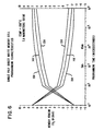
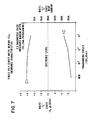
- Figs. 6, 7 and 8 depict representative programming, endurance, and retention characteristics for the nonvolatile memory cell to which this invention pertains.
- a nonvolatile memory cell 100 having vertically arranged bit line 101, responsive to a voltage V B , first write line 102, responsive to a voltage V W1 , and second write line 103, responsive to a voltage V W2 , which vertically oriented lines are respectively connected to row line field effect type access transistors 104, 106 and 107.
- the three access transistors are enabled concurrently by row line 108, which row line provides to each access transistor gate electrode a voltage V R .
- the cell further includes in the series path between access transistor 104 and ground potential a field effect type sense transistor 109.
- the conductive state of sense transistor 109 is defined by the polarity and magnitude of the charge on floating gate electrode 111. Thereby, the presence or absence of specified polarity charge on floating gate electrode 111 can be detected by sensing the conductive path between bit line 101 and ground.
- the selective transfer of charge to or from floating gate electrode 111 is responsive to the magnitude and polarity of the electric field across dielectric layer 112, which is created by the voltages V WI and V W2 on write lines 102 and 103 when access transistors 106 and 107 are enabled.
- the rate at which charge is transferred depends on the highly nonlinear characteristics of the thin dielectric region 112 which separates conductively doped region 113 from extension 114 of floating gate electrode 111.
- dielectric layer 112 is preferably composed of thin, thermally grown silicon dioxide, so as to utilize Fowler-Nordheim tunneling as the primary charge transfer mechanism, it is also possible to employ silicon nitride, silicon oxynitride, or various combinations of the previous named dielectric materials.
- dielectric 112 also creates a capacitor 110 of relatively small value, as specifically established by the thickness and area of dielectric 112 between conductors 113 and 114.
- capacitor 115 is defined by the thickness and area of dielectric 117 situated between conductively doped region 118 and extension 116 of floating gate electrode 111. Though it is preferred, from a process efficiency standpoint that the composition and thickness of dielectric 117 be the same as that of 112, it is feasible to use a different dielectric material and/or thickness to individually adjust the capacitive values of devices 110 and 115. However, secondary effects on retention and endurance should not be overlooked.
- nonvolatile memory cell 100 To understand the operation of nonvolatile memory cell 100, and to more fully appreciate its beneficial features, attention is now directed to Table A.
- the operational voltages set forth in the table are illustrative of those which might used with a cell configured on a silicon wafer with n-channel field effect transistors, using three micron design rules, a dielectric of approximately 7-10 nanometers of thermally grown silicon dioxide for layers 112 and 117, a write/program cycle of approximately 10 milliseconds, and a relative capacitance between capacitors 115 and 110 of approximately 8: 1.
- X-don't care Memory Margining is trademark of NCR Corporation
- the cell according to the present invention in Fig. 2, can be written directly into either data state irrespective of the prior data state. For instance, with reference to Table A, if cell 100 is to be programmed to a "0" data state, the voltage V R is set to be equal to the greater of V WI or V W2 , and in this particular case to 15 volts, V WI is fixed at 0 volts, and V W2 is driven to 15 volts.
- floating gate electrode 111 is capactively coupled to the potential on line 118 by virtue of the relative capacitances of 110 and 115 to impress across thin dielectric layer 112 an electric field proportional to the relative voltage and of a polarity defined by write voltages V W1 and V W2 .
- the polarity of the write voltages define the direction and nature of the charge transferred through dielectric 112. For example, during the writing/ programming of a "0" binary state into cell 100 electrons move through dielectric 112 by FowlerNordheim tunneling from region 114 of floating gate electrode 111 to conductively doped region 113. This results in a net positive charge being retained on floating gate 111 when the write voltage ceases. The positive charge on gate 111 thereafter biases sense transistor 109 to a conductive state. For the writing/programming of a "1", the voltages V W1 and V W2 are reversed, to trap on floating gate 111 a residual negative charge and thereby disable sense transistor
- the state programmed into memory cell 100 is read by biasing V R to 5 volts, while setting V W1 , V W2 and V B to 1 volt. It is also possible to utilize a V B line precharge technique.
- a conventional sense amplifier connected to line 101 is normally used to detect whether sense transistor 109 is conductively biased by charge on floating gate 111.
- nonvolatile memory cell 100 is capable of a Memory Margining TM test, in which the threshold window of the nonvolatile memory cell is individually tested to detect the magnitudes of the 0 or 1 threshold levels.
- V R may set at 5 volts
- V B set at one volt or other appropriate test voltage
- V W1 and V W2 are varied to detect the bias voltage at which sense transistor 109 commences or ceases conduction.
- the relatively large capacitive coupling of lines 113 and 118 to floating gate 111 allows the potential of floating gate 111 to be shifted by an amount equal to the mathematical sum of the previously written floating gate potential due to the charge remaining plus the bias potential.
- nonvolatile memory cell 100 exhibits the highly desirable absence of any read disturb.
- the thin dielectrics 112 and 117 are not subject to the electric field produced by read voltage V B , in that sense transistor 109 and access transistor 104 are situated in a separate conductive path.
- sense voltage V B is never applied to an electrode or conductively doped region common to either a charge transfer dielectric or the relatively large capacitor dielectric. Therefore, the quantity of the charge on floating gate electrode 111 is not diminished by a read operation on cell 100. As was noted earlier, this is extremely important in applications where highly repetitive addressing of the cell data is possible.
- this present cell in distinction from the prior art, is of a direct write configuration, for a single cycle for programming, retains the Memory Margining capability, is configured with a floating gate structure, and can be fabricated in a single poly process with minimum alteration to the fabrication cycle.
- bit line 101 resides in a upper metallization layer defined by the dash lines, and is connected to diffused region 201 by contact 202.
- Diffusion 201 constitutes the drain electrode of field effect transistor 104 formed by the overlying first conductively doped polysilicon layer gate electrode 108, a row line.
- the source electrode of transistor 104 is diffused region 203.
- diffusion 203 which also serves as the drain electrode of sense field effect transistor 109, and ground electrode 204, also a diffused region, there is shown an overlying extension of first polysilicon floating gate electrode 111 operating as the gate electrode of transistor 109.
- nonvolatile memory cell 100 is similarly arranged, beginning with an upper level metal electrode 102 connected by contact 206 to diffused region 207, which diffusion 207 serves as the drain electrode of field effect transistor 106 formed by the overlying, shared polysilicon gate electrode 108.
- conductively doped region 118 serves as the source electrode of field effect transistor 106, where it exists as a diffused region, and an electrically common conductively doped region coextensive with dielectric 117, where it exists as an implanted region.
- conductive region 118 has lateral projections to increase the surface area of capacitor 115. Conductive region 118 is separated from floating gate 111 by a thin dielectric 117, shown by stipple.
- the last of the three columns also includes an upper level metal conductor 103, here connected by way of contact 211 to diffused drain region 212 of field effect transistor 107, which transistor is formed by overlying, shared polysilicon gate electrode 108.
- conductively doped region 113 serves as the source electrode of field effect transistor 107, where it exists as a diffused region, and an electrically common conductively doped region coextensive with dielectric 112, where it exists as an implanted region.
- Extension 114 of polysilicon floating gate electrode 111 is electrically isolated from conductively doped region 113 at the intersection of 113 and 114 by thin dielectric 112 to form capacitor 110. Recall the earlier comparison of the sizes of capacitors 110 and 115, and the charge transfer occurring at 110 between conductively doped region 113 and floating gate electrode 111.
- the layout of Fig. 3 would be formed in a p-type monocrystalline silicon substrate, generally 209, with n-channel field effect transistors.
- the invention is not so limited and is fully suitable for use with CMOS processes involving n-well, p-well or twin tub configurations.
- the electrodes could be formed from any conductive material and fully contemplate the alternate use of refractory metals, silicides and polycides.
- the layout of the structural elements which make up the cell lends itself to a dense arrangement in which the diffusion and metal pitch are matched. Furthermore, the symmetry in the circuit patterns facilitates area efficient arrangements of the cells into matrix arrays.
- the thin dielectrics 112 and 117 be composed of approximately 7-10 nanometers of silicon dioxide thermally grown from the monocrystalline silicon substrate, generally 209, it is also feasible to deposit the silicon dioxide or to use nitride based dielectrics which are either directly deposited or converted from silicon dioxide, including but not limited to thin composite layers of silicon dioxide, silicon nitride, and silicon oxynitride.
- FIG. 5 A functionally similar but structurally different nonvolatile memory cell 300 is depicted schematically in Fig. 4, and by way of layout in Fig. 5.
- sense transistor 301 is situated within the central column of the three.
- the effects of this rearrangement on the structure are more pronounced in the layout depicted in Fig. 5.
- the embodiment depicted in Fig. 5 utilizes a smaller area for the thin dielectric region 302, through which charge is transferred to and removed from poly one level floating gate electrode 303.
- row line electrode 308, which enable access transistors 304, 306 and 307, is a poly one level electrode.
- the embodiment in Fig. 5 employs a relatively thick dielectric 309 to form the coupling capacitor between floating gate electrode 303 and the diffusion 311 extending from the source electrode of field effect transistor 307.
- the dielectric composition and thickness of 309 would be comparable to that used to isolate the gate electrode 308 from the channel regions of field effective transistors 304, 306 and 307.
- the area of charge transfer throug thin dielectric 302 is further reduced in relation to the area of the coupling capacitor 312 in order to maintain a substantially similar ratio of capacitances and thereby insure that the write/program voltage which appears across the thin, charge transfer dielectric 302 is adequate to provide the necessary degree of charge tunneling or conduction.
- the composition of the thin dielectric 302 may be thermally grown or deposited silicon dioxide or a nitride based dielectric.
- Figs. 6, 7 and 8 depict representative performance characteristics for a nonvolatile memory cell of the form depicted in Figs. 2 and 3.
- Cells having such characteristics generally utilize for dielectrics 112 and 117 a 7-10 nanometer thick silicon dioxide layer, which can for example, be formed by thermal oxidation of the substrate silicon in an 02 + 3% HCl ambient at atmospheric pressure and an 800-850°C temperature for approximately 5-10 minutes.
- the ambient would be diluted with argon to more precisely control the oxidation rate.
- the sense transistor threshold voltage used to establish the memory window was measured at a current flow of 20 microamps.
- Fig. 6 shows the effects of programming time and write/program voltages on the memory window.
- An analysis of Fig. 6 discloses that such a cell can be programmed in significantly less time than 10 milliseconds while using write/program voltages which are compatible with normal logic circuit fabrication technologies.
- Fig. 7 The plots of endurance characteristics as depicted in Fig. 7 confirm that the cell to which this invention pertains has a performance comparable to that exhibited by functionally similar commercial products.
- the long term data storage capabilities of the cell are illustrated by the minimal slope in the plots of Fig. 8, where the composite effects of repeated writing/programming and storage time are shown for both "0" and "1" data states.
Landscapes
- Engineering & Computer Science (AREA)
- Microelectronics & Electronic Packaging (AREA)
- Non-Volatile Memory (AREA)
- Read Only Memory (AREA)
Abstract
Description
- This invention relates to nonvolatile memory cells, of the kind including: a floating gate electrode located over the semiconductor substrate; a first conductively doped region in the substrate, situated beneath a first region of the floating gate electrode and separated therefrom by a first dielectric material layer to form thereby a coupling of first capacitance; and a second conductively doped region in the substrata, situated beneath a second region of the floating gate electrode and separated therefrom by a second capacitance, materially less than the first capacitance, and define a region of charge transfer through the second dielectric material layer.
- A nonvolatile memory cell of the kind specified is known from an article by Cuppens et al., entitled "An EEPROM for Microprocessors and Custom Logic," IEEE Journal Solid-State Circuits, Vol. SC-20, No. 2, April 1985, pp 603-608, and from a paper of the same authorship and title published in the Digest of Technical Papers of the 1984 IEEE International Solid State Circuits Conference, pages 268-269.
- The composite cell configuration which these references disclose is schematically depicted on Fig. I of the drawings. As shown there, a
left cell 1, defined by a perimeter of long dashed lines, and aright cell 2, defined by a perimeter of short dashed lines, shareaccess transistor 3 fromwrite line 4 as well astransistor 6, suitable toground conducting path 7.Left cell 1 is further composed ofrow line 8 for simultaneously enablingaccess transistors Transistor 9 when enabled connects bit line 11 toconductive path 12, which conductive path is preferably a source/drain type diffusion joiningaccess transistor 9 to sensetransistor 13. In proximity todiffusion 12, but separated by charge transfer dielectric 14 therefrom, there is situated asegment 16 of conductive floating gate electrode 17, as shown. Floating gate electrode 17 itself extends at the opposite end to a position adjacent similarly diffusedconductive path 18, and is of suitable size and proximity todiffusion 18 to provide by way of dielectric 19 an effective capacitive coupling significantly greater than that created by the proximity ofelectrode segment 16 todiffusion 12. According to the described configuration, 18 is an extension of the source/drain diffusion fortransistor 3. The remaining element inleft side cell 1 isgrounding transistor 6, which connects the diffusion typeconductive path 7 to ground potential upon receiving an enablement signal online 21. - One detracting feature of the paired cell depicted in Fig. 1 is the lack of capability to directly write either cell, or stated otherwise, the inability to program the state of the cell to a binary 0 or 1 without undergoing a preceding erase operation. This is attributable to the fact that the
coupling capacitors share line 18, and thereby couple thesame line 18 potential to both floating gates. This requires that the potential online 18 remain fixed during the.write/program operation for the data in the non-selected cell to remain intact. Voltages VB0 and VB1 are the variables during the write cycle, and the write operation can only transfer charge in one direction. Therefore, this configuration requires that both cells be erased before writing new data into either of the two cells. As one of skill in the art will appreciate, the need for both erase and write cycles to effect the entry of data into a cell, in contrast to a single direct write cycle, increases the functional complexity of the operations to be performed on the chip, and consequently the chip area consumed by the timing and control circuitry. - The two cell configuration depicted in Fig. 1 also suffers from another disadvantage, the potential for having the nonvolatily stored data disturbed during a read cycle if the read cycle bit line, e.g. VB1, and write line voltages, are not the same. The use of such different voltages for e.g. VB1 and VW is not uncommon with floating gate devices in that it allows for the centering of the reference level within the memory window. Even minimal amounts of read disturb are considered highly undesirable when repeated read addressing of the cell is possible, such as is common in high clock rate microprocessors operating in looped cycles. On the other hand, the ability to selectively set the voltages e.g. VB1 and VW during the read cycle is a desirable feature if the nonvolatile data is to be stored and reliably retrieved over an extended time period, namely when the memory window shrinks.
- From US-A-4 288 863, there is known a nonvolatile memory cell including a floating gate electrode which has a first region separated from a first conductively doped substrate region by a first insulating layer to form a first capacitance, a second region separated from a second conductively doped substrate region by a second insulating layer to form a second capacitance, with the first capacitance being greater than the second capacitance, and a third region which forms the gate of a read transistor having source and drain regions in the substrate. The first and second conductively doped substrate regions are conected by respective write and erase transistors to respective write and read lines. The gate electrodes of the write and read transistors are connected to a row decoding line.
- It is an object of the present invention to provide a nonvolatile memory cell of the kind specified, wherein the aforementioned disadvantages are alleviated.
- Therefore, according to the present invention, there is provided a nonvolatile memory cell formed on a semiconductor substrate, including: a floating gate electrode located over the semiconductor substrate a first conductively doped region in the substrate, situated beneath a first region of the floating gate electrode and separated therefrom by a first dielectric material layer to form thereby a coupling of first capacitance; and a second conductively doped region in the substrate, situated beneath a second region of the floating gate electrode and separated therefrom by a second dielectric material layer to form a coupling of second capacitance, materially less than the first capacitance, and define a region of charge transfer through the second dielectric material layer, third and fourth conductively doped regions in the substrate which are electrically isolated from the first and second conductively doped regions, defining therebetween a channel situated beneath a third region of the floating gate electrode and separated therefrom by a third dielectric material layer, to form a field effect transistor responsive to the charge resident on the floating gate electrode; access means for selectively connecting the first conductively doped region in the substrate to a first write line, and selectively connecting the second conductively doped region in the substrate to a second write line; and means for selectively applying potentials of first relative polarity between the first and second write lines suitable to cause a transfer of charge in one direction through the second dielectric material layer, or of a second relative polarity between the first and second write lines to cause a transfer of charge in the opposite direction through the second dielectric material layer, characterized in that said access means is further adapted for selectively connecting the third conductively doped region in the substrate to a bit line.
- It will be appreciated that a nonvolatile memory cell according to the present invention provides both a direct write capability and a absence of any read disturb, while retaining a single floating gate structure, compatible with conventional integrated circuit fabrication processes.
- Two embodiments of the present invention will now be described by way of example, with reference to the accompanying drawings, in which :
- Fig. 1 is an electrical schematic for a floating gate nonvolatile memory device of the prior art, involving two, individually addressable but structurally interrelated single poly floating gate cells.
- Fig. 2 is an electrical schematic of the preferred nonvolatile memory cell according to the present invention, now including the direct write and no read disturb capabilities in a single poly floating gate configuration.
- Fig. 3 is a layout pattern for the cell schematically depicted in Fig. 2.
- Fig. 4 is the electrical schematic for the alternate embodiment of the cell to which this invention pertains.
- Fig. 5 is a layout of the embodiment shown in Fig. 4.
- Figs. 6, 7 and 8 depict representative programming, endurance, and retention characteristics for the nonvolatile memory cell to which this invention pertains.
- Directing attention to Fig. 2, there is shown schematically a
nonvolatile memory cell 100 having vertically arrangedbit line 101, responsive to a voltage VB,first write line 102, responsive to a voltage VW1, andsecond write line 103, responsive to a voltage VW2, which vertically oriented lines are respectively connected to row line field effecttype access transistors row line 108, which row line provides to each access transistor gate electrode a voltage VR. The cell further includes in the series path betweenaccess transistor 104 and ground potential a field effecttype sense transistor 109. The conductive state ofsense transistor 109 is defined by the polarity and magnitude of the charge on floating gate electrode 111. Thereby, the presence or absence of specified polarity charge on floating gate electrode 111 can be detected by sensing the conductive path betweenbit line 101 and ground. - The selective transfer of charge to or from floating gate electrode 111 is responsive to the magnitude and polarity of the electric field across
dielectric layer 112, which is created by the voltages VWI and VW2 onwrite lines access transistors dielectric region 112 which separates conductively dopedregion 113 fromextension 114 of floating gate electrode 111. Thoughdielectric layer 112 is preferably composed of thin, thermally grown silicon dioxide, so as to utilize Fowler-Nordheim tunneling as the primary charge transfer mechanism, it is also possible to employ silicon nitride, silicon oxynitride, or various combinations of the previous named dielectric materials. The nitride based materials provide for transfers of charge by Poole-Frenkel conduction, and as such, allow higher charge transfer rates, and therefore shorter cell write/programming cycle times. Note that dielectric 112 also creates acapacitor 110 of relatively small value, as specifically established by the thickness and area of dielectric 112 betweenconductors - The creation of the electric field across dielectric 112 upon the application of write voltages VWI and VW2 and conduction of
transistors capacitor 110, with dielectric 112, andcapacitor 115, formed with dielectric 117. As embodied and depicted,capacitor 115 is defined by the thickness and area of dielectric 117 situated between conductively dopedregion 118 andextension 116 of floating gate electrode 111. Though it is preferred, from a process efficiency standpoint that the composition and thickness of dielectric 117 be the same as that of 112, it is feasible to use a different dielectric material and/or thickness to individually adjust the capacitive values ofdevices - To understand the operation of
nonvolatile memory cell 100, and to more fully appreciate its beneficial features, attention is now directed to Table A. The operational voltages set forth in the table are illustrative of those which might used with a cell configured on a silicon wafer with n-channel field effect transistors, using three micron design rules, a dielectric of approximately 7-10 nanometers of thermally grown silicon dioxide forlayers capacitors 
X-don't care Memory Margining is trademark of NCR Corporation - In contrast to nonvolatile memory cells having the arrangement depicted in Fig. 1, which as was specifically noted earlier require an erase cycle before initiating a write/program cycle, the cell according to the present invention, in Fig. 2, can be written directly into either data state irrespective of the prior data state. For instance, with reference to Table A, if
cell 100 is to be programmed to a "0" data state, the voltage VR is set to be equal to the greater of VWI or VW2, and in this particular case to 15 volts, VWI is fixed at 0 volts, and VW2 is driven to 15 volts. Upon the lapse of the write/program time interval, the voltages ondiffusions memory cell 100 by reversing the voltages on VW1 and VW2 during the write/program cycle. - Under both write/program conditions floating gate electrode 111 is capactively coupled to the potential on
line 118 by virtue of the relative capacitances of 110 and 115 to impress across thindielectric layer 112 an electric field proportional to the relative voltage and of a polarity defined by write voltages VW1 and VW2. - The polarity of the write voltages define the direction and nature of the charge transferred through dielectric 112. For example, during the writing/ programming of a "0" binary state into
cell 100 electrons move through dielectric 112 by FowlerNordheim tunneling fromregion 114 of floating gate electrode 111 to conductively dopedregion 113. This results in a net positive charge being retained on floating gate 111 when the write voltage ceases. The positive charge on gate 111 thereafter biases sensetransistor 109 to a conductive state. For the writing/programming of a "1", the voltages VW1 and VW2 are reversed, to trap on floating gate 111 a residual negative charge and thereby disable sense transistor - As further shown in Table A, the state programmed into
memory cell 100 is read by biasing VR to 5 volts, while setting VW1, VW2 and VB to 1 volt. It is also possible to utilize a VB line precharge technique. A conventional sense amplifier connected toline 101 is normally used to detect whethersense transistor 109 is conductively biased by charge on floating gate 111. - Table A also discloses that
nonvolatile memory cell 100 is capable of a Memory Margining TM test, in which the threshold window of the nonvolatile memory cell is individually tested to detect the magnitudes of the 0 or 1 threshold levels. For example, as set forth in Table A, VR may set at 5 volts, VB set at one volt or other appropriate test voltage, while VW1 and VW2 are varied to detect the bias voltage at whichsense transistor 109 commences or ceases conduction. The relatively large capacitive coupling oflines - Foremost, it should be understood and appreciated that
nonvolatile memory cell 100 exhibits the highly desirable absence of any read disturb. Note, that according to the arrangement depicted in Fig. 2 thethin dielectrics sense transistor 109 andaccess transistor 104 are situated in a separate conductive path. For instance, with reference to the prior art in Fig. 1, if VBO were set at 1 volt and VW were set to 0 volts dielectric 14 would be subject to a relative electric field, while according to the present invention, as embodied in Fig. 2, sense voltage VB is never applied to an electrode or conductively doped region common to either a charge transfer dielectric or the relatively large capacitor dielectric. Therefore, the quantity of the charge on floating gate electrode 111 is not diminished by a read operation oncell 100. As was noted earlier, this is extremely important in applications where highly repetitive addressing of the cell data is possible. - In addition to this particularly important feature of the present memory cell configuration, recall that this present cell, in distinction from the prior art, is of a direct write configuration, for a single cycle for programming, retains the Memory Margining capability, is configured with a floating gate structure, and can be fabricated in a single poly process with minimum alteration to the fabrication cycle.
- To more fully appreciate the structural arrangement of the
memory cell 100 and any related implications on cell fabrication, there is shown in Fig. 3 a layout of a representative cell which implements the features ascribed to the cell shown schematically in Fig. 2. Functionally corresponding parts are identified by the same reference numerals. As viewed,bit line 101 resides in a upper metallization layer defined by the dash lines, and is connected to diffusedregion 201 bycontact 202.Diffusion 201 constitutes the drain electrode offield effect transistor 104 formed by the overlying first conductively doped polysiliconlayer gate electrode 108, a row line. The source electrode oftransistor 104 is diffusedregion 203. Betweendiffusion 203, which also serves as the drain electrode of sensefield effect transistor 109, andground electrode 204, also a diffused region, there is shown an overlying extension of first polysilicon floating gate electrode 111 operating as the gate electrode oftransistor 109. - The middle column of
nonvolatile memory cell 100 is similarly arranged, beginning with an upperlevel metal electrode 102 connected bycontact 206 to diffusedregion 207, whichdiffusion 207 serves as the drain electrode offield effect transistor 106 formed by the overlying, sharedpolysilicon gate electrode 108. As embodied, conductively dopedregion 118 serves as the source electrode offield effect transistor 106, where it exists as a diffused region, and an electrically common conductively doped region coextensive withdielectric 117, where it exists as an implanted region. As shown in Fig. 3,conductive region 118 has lateral projections to increase the surface area ofcapacitor 115.Conductive region 118 is separated from floating gate 111 by athin dielectric 117, shown by stipple. - The last of the three columns, also includes an upper
level metal conductor 103, here connected by way ofcontact 211 to diffuseddrain region 212 offield effect transistor 107, which transistor is formed by overlying, sharedpolysilicon gate electrode 108. As embodied, conductively dopedregion 113 serves as the source electrode offield effect transistor 107, where it exists as a diffused region, and an electrically common conductively doped region coextensive withdielectric 112, where it exists as an implanted region.Extension 114 of polysilicon floating gate electrode 111 is electrically isolated from conductively dopedregion 113 at the intersection of 113 and 114 bythin dielectric 112 to formcapacitor 110. Recall the earlier comparison of the sizes ofcapacitors doped region 113 and floating gate electrode 111. - Preferably, the layout of Fig. 3 would be formed in a p-type monocrystalline silicon substrate, generally 209, with n-channel field effect transistors. However, the invention is not so limited and is fully suitable for use with CMOS processes involving n-well, p-well or twin tub configurations. Likewise, though reference is made to a doped first polysilicon layer and an upper metallization layer, the electrodes could be formed from any conductive material and fully contemplate the alternate use of refractory metals, silicides and polycides.
- Note that the layout of the structural elements which make up the cell lends itself to a dense arrangement in which the diffusion and metal pitch are matched. Furthermore, the symmetry in the circuit patterns facilitates area efficient arrangements of the cells into matrix arrays.
- Though it is preferred that the
thin dielectrics - A functionally similar but structurally different
nonvolatile memory cell 300 is depicted schematically in Fig. 4, and by way of layout in Fig. 5. In this case,sense transistor 301 is situated within the central column of the three. The effects of this rearrangement on the structure are more pronounced in the layout depicted in Fig. 5. As a further element of difference, the embodiment depicted in Fig. 5 utilizes a smaller area for the thindielectric region 302, through which charge is transferred to and removed from poly one level floatinggate electrode 303. Again, as was true of the cell depicted in Figs. 2 and 3,row line electrode 308, which enableaccess transistors gate electrode 303 and thediffusion 311 extending from the source electrode offield effect transistor 307. According to this practice of the invention, the dielectric composition and thickness of 309 would be comparable to that used to isolate thegate electrode 308 from the channel regions of fieldeffective transistors thin dielectric 302 is further reduced in relation to the area of thecoupling capacitor 312 in order to maintain a substantially similar ratio of capacitances and thereby insure that the write/program voltage which appears across the thin,charge transfer dielectric 302 is adequate to provide the necessary degree of charge tunneling or conduction. - Again, as was true of the embodiment set forth in Figs. 2 and 3, the composition of the
thin dielectric 302 may be thermally grown or deposited silicon dioxide or a nitride based dielectric. - Figs. 6, 7 and 8 depict representative performance characteristics for a nonvolatile memory cell of the form depicted in Figs. 2 and 3. Cells having such characteristics generally utilize for
dielectrics 112 and 117 a 7-10 nanometer thick silicon dioxide layer, which can for example, be formed by thermal oxidation of the substrate silicon in an 02 + 3% HCl ambient at atmospheric pressure and an 800-850°C temperature for approximately 5-10 minutes. Preferably, the ambient would be diluted with argon to more precisely control the oxidation rate. For the depicted characteristics the sense transistor threshold voltage used to establish the memory window was measured at a current flow of 20 microamps. - Fig. 6 shows the effects of programming time and write/program voltages on the memory window. An analysis of Fig. 6 discloses that such a cell can be programmed in significantly less time than 10 milliseconds while using write/program voltages which are compatible with normal logic circuit fabrication technologies.
- The plots of endurance characteristics as depicted in Fig. 7 confirm that the cell to which this invention pertains has a performance comparable to that exhibited by functionally similar commercial products. The long term data storage capabilities of the cell are illustrated by the minimal slope in the plots of Fig. 8, where the composite effects of repeated writing/programming and storage time are shown for both "0" and "1" data states.
Claims (10)
Applications Claiming Priority (2)
| Application Number | Priority Date | Filing Date | Title |
|---|---|---|---|
| US775980 | 1985-09-13 | ||
| US06/775,980 US4683554A (en) | 1985-09-13 | 1985-09-13 | Direct write nonvolatile memory cells |
Publications (2)
| Publication Number | Publication Date |
|---|---|
| EP0238549A1 EP0238549A1 (en) | 1987-09-30 |
| EP0238549B1 true EP0238549B1 (en) | 1991-02-27 |
Family
ID=25106111
Family Applications (1)
| Application Number | Title | Priority Date | Filing Date |
|---|---|---|---|
| EP86905620A Expired EP0238549B1 (en) | 1985-09-13 | 1986-09-08 | Nonvolatile memory cell |
Country Status (4)
| Country | Link |
|---|---|
| US (1) | US4683554A (en) |
| EP (1) | EP0238549B1 (en) |
| JP (1) | JP2578786B2 (en) |
| WO (1) | WO1987001859A2 (en) |
Families Citing this family (23)
| Publication number | Priority date | Publication date | Assignee | Title |
|---|---|---|---|---|
| FR2599176A1 (en) * | 1986-05-23 | 1987-11-27 | Eurotechnique Sa | MEMORY DEADLY PROGRAMMABLE ELECTRICALLY |
| US4754432A (en) * | 1986-07-25 | 1988-06-28 | Ncr Corporation | Nonvolatile multiconfigurable circuit |
| US4769788A (en) * | 1986-09-22 | 1988-09-06 | Ncr Corporation | Shared line direct write nonvolatile memory cell array |
| US4914627A (en) * | 1987-07-02 | 1990-04-03 | Ramtron Corporation | One transistor memory cell with programmable capacitance divider |
| US4910708A (en) * | 1987-07-02 | 1990-03-20 | Ramtron Corporation | Dram with programmable capacitance divider |
| US4918654A (en) * | 1987-07-02 | 1990-04-17 | Ramtron Corporation | SRAM with programmable capacitance divider |
| US4853893A (en) * | 1987-07-02 | 1989-08-01 | Ramtron Corporation | Data storage device and method of using a ferroelectric capacitance divider |
| JP2664685B2 (en) * | 1987-07-31 | 1997-10-15 | 株式会社東芝 | Method for manufacturing semiconductor device |
| US5315547A (en) * | 1988-07-11 | 1994-05-24 | Hitachi, Ltd. | Nonvolatile semiconductor memory device with selective tow erasure |
| JP2580752B2 (en) * | 1988-12-27 | 1997-02-12 | 日本電気株式会社 | Nonvolatile semiconductor memory device |
| JP2529885B2 (en) * | 1989-03-10 | 1996-09-04 | 工業技術院長 | Semiconductor memory and operating method thereof |
| US5168464A (en) * | 1989-11-29 | 1992-12-01 | Ncr Corporation | Nonvolatile differential memory device and method |
| US5097444A (en) * | 1989-11-29 | 1992-03-17 | Rohm Corporation | Tunnel EEPROM with overerase protection |
| US5057447A (en) * | 1990-07-09 | 1991-10-15 | Texas Instruments Incorporated | Silicide/metal floating gate process |
| US5355007A (en) * | 1990-11-23 | 1994-10-11 | Texas Instruments Incorporated | Devices for non-volatile memory, systems and methods |
| US5412599A (en) * | 1991-09-26 | 1995-05-02 | Sgs-Thomson Microelectronics, S.R.L. | Null consumption, nonvolatile, programmable switch |
| US6077750A (en) * | 1998-10-27 | 2000-06-20 | Lg Semicon Co., Ltd. | Method for forming epitaxial Co self-align silicide for semiconductor device |
| US6087236A (en) * | 1998-11-24 | 2000-07-11 | Intel Corporation | Integrated circuit with multiple gate dielectric structures |
| US7269090B2 (en) | 2001-01-30 | 2007-09-11 | Freescale Semiconductor, Inc. | Memory access with consecutive addresses corresponding to different rows |
| DE102006024121B4 (en) * | 2006-05-22 | 2011-02-24 | Telefunken Semiconductors Gmbh & Co. Kg | Nonvolatile memory cell of a circuit integrated in a semiconductor chip, method for its production and use of a nonvolatile memory cell |
| US7439567B2 (en) * | 2006-08-09 | 2008-10-21 | Atmel Corporation | Contactless nonvolatile memory array |
| DE102006038936A1 (en) * | 2006-08-18 | 2008-02-28 | Atmel Germany Gmbh | Switching regulator, transceiver circuit and keyless access control system |
| US8320191B2 (en) | 2007-08-30 | 2012-11-27 | Infineon Technologies Ag | Memory cell arrangement, method for controlling a memory cell, memory array and electronic device |
Family Cites Families (7)
| Publication number | Priority date | Publication date | Assignee | Title |
|---|---|---|---|---|
| NL7500550A (en) * | 1975-01-17 | 1976-07-20 | Philips Nv | SEMICONDUCTOR MEMORY DEVICE. |
| DE2743422A1 (en) * | 1977-09-27 | 1979-03-29 | Siemens Ag | Word-wise erasable, non-volatile memory in floating gate technology |
| DE2916884C3 (en) * | 1979-04-26 | 1981-12-10 | Deutsche Itt Industries Gmbh, 7800 Freiburg | Programmable semiconductor memory cell |
| DE3031748A1 (en) * | 1979-08-24 | 1982-03-04 | Centre Electronique Horloger S.A., Neuchâtel | ELECTRICALLY ERASABLE AND REPEAT PROGRAMMABLE STORAGE ELEMENT FOR PERMANENT STORAGE |
| US4531203A (en) * | 1980-12-20 | 1985-07-23 | Tokyo Shibaura Denki Kabushiki Kaisha | Semiconductor memory device and method for manufacturing the same |
| JPS5878170A (en) * | 1981-11-04 | 1983-05-11 | Toshiba Corp | Exposure device |
| US4546454A (en) * | 1982-11-05 | 1985-10-08 | Seeq Technology, Inc. | Non-volatile memory cell fuse element |
-
1985
- 1985-09-13 US US06/775,980 patent/US4683554A/en not_active Expired - Lifetime
-
1986
- 1986-09-08 WO PCT/US1986/001825 patent/WO1987001859A2/en not_active Ceased
- 1986-09-08 JP JP61504808A patent/JP2578786B2/en not_active Expired - Lifetime
- 1986-09-08 EP EP86905620A patent/EP0238549B1/en not_active Expired
Also Published As
| Publication number | Publication date |
|---|---|
| JP2578786B2 (en) | 1997-02-05 |
| JPS63500908A (en) | 1988-03-31 |
| EP0238549A1 (en) | 1987-09-30 |
| US4683554A (en) | 1987-07-28 |
| WO1987001859A2 (en) | 1987-03-26 |
| WO1987001859A3 (en) | 1987-06-18 |
Similar Documents
| Publication | Publication Date | Title |
|---|---|---|
| US4683554A (en) | Direct write nonvolatile memory cells | |
| US5978253A (en) | Methods of operating integrated circuit memory devices having nonvolatile single transistor unit cells therein | |
| US5389567A (en) | Method of forming a non-volatile DRAM cell | |
| US4300212A (en) | Nonvolatile static random access memory devices | |
| US4907198A (en) | Semiconductor memory device | |
| US4334292A (en) | Low voltage electrically erasable programmable read only memory | |
| US4888630A (en) | Floating-gate transistor with a non-linear intergate dielectric | |
| US5483484A (en) | Electrically erasable programmable read-only memory with an array of one-transistor memory cells | |
| EP0042964B1 (en) | Memory matrix using one-transistor floating gate mos cells | |
| US4654828A (en) | Nonvolatile semiconductor memory | |
| CA1218151A (en) | Semiconductor memory | |
| EP0467928A1 (en) | NOVRAMZELL USING TWO DIFFERENTIAL UNCOUPLABLE NON-VOLATILE MEMORY ELEMENTS. | |
| RU2216819C2 (en) | Semiconductor storage | |
| US7518177B2 (en) | Semiconductor storage device | |
| US5355332A (en) | Electrically erasable programmable read-only memory with an array of one-transistor memory cells | |
| EP0282528B1 (en) | Nonvolatile memory cell | |
| EP0281597B1 (en) | Nonvolatile memory cell array | |
| JP3251699B2 (en) | Non-volatile storage device | |
| KR910009452B1 (en) | Integrated Circuit with Dynamic Memory Cells | |
| US5134450A (en) | Parallel transistor circuit with non-volatile function | |
| Koike et al. | New two-terminal C-MNOS memory cells | |
| JPH04123470A (en) | Nonvolatile semiconductor memory | |
| JPH06112498A (en) | Ferroelectric nonvolatile memory structure and manufacture thereof | |
| JPS6182460A (en) | Nonvolatile semiconductor memory device | |
| JPH11251462A (en) | Nonvolatile semiconductor memory device |
Legal Events
| Date | Code | Title | Description |
|---|---|---|---|
| PUAI | Public reference made under article 153(3) epc to a published international application that has entered the european phase |
Free format text: ORIGINAL CODE: 0009012 |
|
| AK | Designated contracting states |
Kind code of ref document: A1 Designated state(s): DE GB NL |
|
| 17P | Request for examination filed |
Effective date: 19871127 |
|
| DET | De: translation of patent claims | ||
| 17Q | First examination report despatched |
Effective date: 19890804 |
|
| GRAA | (expected) grant |
Free format text: ORIGINAL CODE: 0009210 |
|
| AK | Designated contracting states |
Kind code of ref document: B1 Designated state(s): DE GB NL |
|
| REF | Corresponds to: |
Ref document number: 3677766 Country of ref document: DE Date of ref document: 19910404 |
|
| PLBE | No opposition filed within time limit |
Free format text: ORIGINAL CODE: 0009261 |
|
| STAA | Information on the status of an ep patent application or granted ep patent |
Free format text: STATUS: NO OPPOSITION FILED WITHIN TIME LIMIT |
|
| 26N | No opposition filed | ||
| REG | Reference to a national code |
Ref country code: GB Ref legal event code: 732 |
|
| NLS | Nl: assignments of ep-patents |
Owner name: SAMSUNG ELECTRONICS CO., LTD. TE SEOUL, ZUID-KOREA |
|
| REG | Reference to a national code |
Ref country code: GB Ref legal event code: IF02 |
|
| PGFP | Annual fee paid to national office [announced via postgrant information from national office to epo] |
Ref country code: DE Payment date: 20050902 Year of fee payment: 20 |
|
| PGFP | Annual fee paid to national office [announced via postgrant information from national office to epo] |
Ref country code: NL Payment date: 20050904 Year of fee payment: 20 |
|
| PGFP | Annual fee paid to national office [announced via postgrant information from national office to epo] |
Ref country code: GB Payment date: 20050907 Year of fee payment: 20 |
|
| REG | Reference to a national code |
Ref country code: GB Ref legal event code: PE20 |
|
| PG25 | Lapsed in a contracting state [announced via postgrant information from national office to epo] |
Ref country code: GB Free format text: LAPSE BECAUSE OF EXPIRATION OF PROTECTION Effective date: 20060907 |
|
| PG25 | Lapsed in a contracting state [announced via postgrant information from national office to epo] |
Ref country code: NL Free format text: LAPSE BECAUSE OF EXPIRATION OF PROTECTION Effective date: 20060908 |
|
| NLV7 | Nl: ceased due to reaching the maximum lifetime of a patent |
Effective date: 20060908 |