EP0238283A2 - High voltage detecting circuit - Google Patents
High voltage detecting circuit Download PDFInfo
- Publication number
- EP0238283A2 EP0238283A2 EP87302223A EP87302223A EP0238283A2 EP 0238283 A2 EP0238283 A2 EP 0238283A2 EP 87302223 A EP87302223 A EP 87302223A EP 87302223 A EP87302223 A EP 87302223A EP 0238283 A2 EP0238283 A2 EP 0238283A2
- Authority
- EP
- European Patent Office
- Prior art keywords
- potential
- semiconductor device
- electrodes
- transistor
- circuit
- Prior art date
- Legal status (The legal status is an assumption and is not a legal conclusion. Google has not performed a legal analysis and makes no representation as to the accuracy of the status listed.)
- Granted
Links
Images


Classifications
-
- G—PHYSICS
- G01—MEASURING; TESTING
- G01R—MEASURING ELECTRIC VARIABLES; MEASURING MAGNETIC VARIABLES
- G01R19/00—Arrangements for measuring currents or voltages or for indicating presence or sign thereof
-
- H—ELECTRICITY
- H03—ELECTRONIC CIRCUITRY
- H03K—PULSE TECHNIQUE
- H03K17/00—Electronic switching or gating, i.e. not by contact-making and –breaking
- H03K17/22—Modifications for ensuring a predetermined initial state when the supply voltage has been applied
- H03K17/223—Modifications for ensuring a predetermined initial state when the supply voltage has been applied in field-effect transistor switches
-
- G—PHYSICS
- G01—MEASURING; TESTING
- G01R—MEASURING ELECTRIC VARIABLES; MEASURING MAGNETIC VARIABLES
- G01R19/00—Arrangements for measuring currents or voltages or for indicating presence or sign thereof
- G01R19/165—Indicating that current or voltage is either above or below a predetermined value or within or outside a predetermined range of values
- G01R19/16504—Indicating that current or voltage is either above or below a predetermined value or within or outside a predetermined range of values characterised by the components employed
- G01R19/16519—Indicating that current or voltage is either above or below a predetermined value or within or outside a predetermined range of values characterised by the components employed using FET's
-
- G—PHYSICS
- G01—MEASURING; TESTING
- G01R—MEASURING ELECTRIC VARIABLES; MEASURING MAGNETIC VARIABLES
- G01R31/00—Arrangements for testing electric properties; Arrangements for locating electric faults; Arrangements for electrical testing characterised by what is being tested not provided for elsewhere
- G01R31/28—Testing of electronic circuits, e.g. by signal tracer
- G01R31/317—Testing of digital circuits
- G01R31/31701—Arrangements for setting the Unit Under Test [UUT] in a test mode
-
- H—ELECTRICITY
- H03—ELECTRONIC CIRCUITRY
- H03K—PULSE TECHNIQUE
- H03K17/00—Electronic switching or gating, i.e. not by contact-making and –breaking
- H03K17/22—Modifications for ensuring a predetermined initial state when the supply voltage has been applied
-
- H—ELECTRICITY
- H03—ELECTRONIC CIRCUITRY
- H03K—PULSE TECHNIQUE
- H03K5/00—Manipulating of pulses not covered by one of the other main groups of this subclass
- H03K5/153—Arrangements in which a pulse is delivered at the instant when a predetermined characteristic of an input signal is present or at a fixed time interval after this instant
Definitions
- the present invention relates to a high voltage detecting circuit, and in particular, to a high voltage detecting circuit included in a semiconductor device having terminals, for generating a control signal to start a specific operating mode of the semiconductor device, when the potential of a specific mode signal higher by a predetermined value then a normal input voltage having a predetermined range, is applied to at least one of the terminals of the semiconductor device.
- a high voltage detecting circuit is included in a semiconductor device for detecting a potential of a terminal of the semiconductor device.
- the high voltage detecting circuit When the potential of the terminal of the device is higher by a predetermined value than a normal input voltage having a predetermined range, the high voltage detecting circuit generates a control signal for starting a specific mode of the semiconductor device. Upon receiving the control signal, the semiconductor device changes to the specific mode, e.g., a testing mode.
- a high voltage detecting circuit is disclosed in, for example, JP-A-60-124124 and comprises
- the prior high voltage detecting circuit When a potential of a power line (hereinafter referred to as a power line potential) of the semiconductor device is stable the prior high voltage detecting circuit, as in JP-A-60-124124 generates or does not generate the control signal exactly in accordance with the potential applied from an another device to the terminal of the semiconductor device. That is, when the potential of the terminal of the semiconductor device is within the predetermined range of the normal input voltage, the prior high voltage detecting circuit does not generate the control signal for starting the specific mode of the device. However, when the potential of the terminal or the semiconductor device is higher by the predetermined value than the normal input voltage, the prior high voltage detecting circuit generates the control signal and the semiconductor device changes to the specific mode, e.g., to the testing mode.
- the normal mode signal of the terminal of the semiconductor device may be higher by the predetermined value than the increased power line potential. That is, the normal signal of the normal input voltage is considered to be the control signal for starting the specific mode of the semiconductor device. Consequently, the prior high voltage detecting circuit may generate a control signal in error without receiving the specific mode signal, and the semiconductor device may be changed to the specific mode by the erroneous control signal.
- such a high voltage detecting circuit includes level shift means having an input end and an output end, the input end being connected to the other of the two other electrodes of the blocking transistor, the level shift means obtaining a potential at the output end lower by a level shifted value than the potential at its input end; and,
- resistor means having a first end and a second end, the first end being connected to the output end of the level shift means and the second end being connected to the second power supply means, the first end of the discrimination circuit being connected to the output end of the level shift means and to the first end of the resistor means;
- the resistor means keeping the potential of the first end at the low potential of the second power supply means when the potential of the at least one of the terminals is within the predetermined range of the normal input voltage.
- the level shift means may include at least one MIS transistor, having a control electrode and two other electrodes.
- the control electrode is operatively connected to one of the two other electrodes.
- the other of the two other electrodes is operatively connected to the first end of the resistor means.
- the level shift value is determined by the threshold voltage of at lest one MIS transistor.
- the resistor means may include a depletion type MIS transistor, having a control electrode and two other electrodes.
- the control electrode is operatively connected to one of the two other electrodes and to the second power supply means.
- the other of the two other electrodes is operatively connected to at least one of the terminals of the semiconductor device, for keeping a leakage current under a predetermined standard current of the semiconductor device.
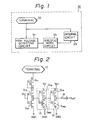
- Figure I is a block diagram illustrating a semiconductor device including a high voltage detecting circuit.
- a terminal 32 of a semiconductor device 30 is connected to an internal circuit 35 and a signal of the terminal 32 is transmitted directly to the internal circuit 35.
- the terminal 32 is also connected to a high voltage detecting circuit 31.
- the high voltage detecting circuit 31 When a potential of a specific mode signal higher by a predetermined value than a normal voltage having a predetermined range is applied to the terminal 32 of the semiconductor device 30, the high voltage detecting circuit 31 generates a control signal.
- the control signal is transmitted to a specific mode circuit 33, and the specific mode circuit 33 makes the internal circuit 35, to a specific mode. That is, when the specific mode signal is applied to the terminal 32 of the semiconductor device 30, the semiconductor device 30 changes to the specific mode, e.g., a testing mode.
- FIG. 2 is a circuit diagram of an example of a conventional high voltage detecting circuit.
- the high voltage detecting circuit is included in a semiconductor device as in the above description with reference to Fig. I.
- a specific mode signal e.g., 8 volts
- a normal input voltage having a predetermined range e.g., from 0 volt to 5 volts
- a source of a leakage current cutting off transistor Q 11 which is a P-channel type MIS transistor, is connected to the terminal 12 of the semiconductor device, and a gate and drain of the transistor Q 11 are connected commonly to a source of a P type MIS transistor Q 13 .
- a gate and a drain of the transistor Q 13 are connected to a gate and a drain of an N-channel type MIS transistor Qi4, respectively, and a source of the transistor Q 14 is connected to a ground GND.
- a common gate of both transistors Q 13 and Q 14 is connected to a power line Vcc (the reference mark Vcc also indicates a power line potential).
- a common drain of both transistors Q 13 and Q 14 is connected to a common gate of a first inverter circuit 15 consisting of a P type M18 transistor Q 151 and an N type MIS transistor Q 152 .
- a common drain of the first inverter circuit 15 is connected to a common gate of a second inverter circuit 16 consisting of a P type MIS transistor Q 161 and an N type MIS transistor Q 162 .
- a common drain of the second inverter circuit 16 is an output end 19 of the high voltage detecting circuit and the control signal S 01 is transmitted from the output end 19 to the internal circuit through the specific mode circuit of the semiconductor device.
- sources of the transistor Q 151 and Q 161 are connected to the power line Vcc and sources of the transistor Q 152 and Q 162 are connected to the ground GND.
- the high voltage detecting circuit when the power line potential Vcc is stabilized, e.g., 5 volts, and a normal mode signal within the normal input voltage, e.g., from 0 volt to 5 volts, is applied to the terminal 12, the high voltage detecting circuit does not generate the control signal. Because a potential of the source of the transistor Q 13 is not higher by the threshold voltage of the transistor Q 13 than a potential of the gate of the transistor 0 13 , the transistor Qi 3 is not switched ON.
- a potential of the common gate of the first inverter circuit 15 is at a low level
- a potential of the common gate of the second inverter circuit 16 is at a high level
- the output end 19 of the high voltage detecting circuit is at the low level. That is, the control signal S 01 is not generated and the semiconductor device continues in a normal mode operation.
- the high voltage detecting circuit When the power line potential Vcc is stabilized, e.g., 5 volts, and the specific mode signal, e.g., 8 volts, higher by a predetermined value than the normal input voltage is applied to the terminal 12, the high voltage detecting circuit generates the control signal. Because a potential of the source of the transistor Q 13 is higher by the threshold voltage of the transistor Q 13 than a potential of the gate of the transistor Q 13 , the transistor Q 13 is switched ON. Consequently, a potential of the common gate of the first inverter circuit 15 is at the high level, a potential of the common gate of the second inverter circuit 16 is at the low level, and the output end 19 of the high voltage detecting circuit is at the high level. That is, the staring signal S 01 is generated and the semiconductor device changes to the specific mode operation.
- the specific mode signal e.g. 8 volts
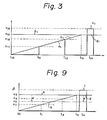
- Figure 3 is a graph illustrating the conventional high voltage detecting circuit shown in Fig. 2 at the time of switching ON the semiconductor device.
- the power line potential Vcc is gradually increased from 0 volt at the time t 10 to the stabilized power line potential V 10 (e.g., 5 volts) at a time t 13 , shown by a line a 1 in Fig. 3, until the power line potential Vcc is stabilized.
- the normal mode signal of the normal input voltage e.g., under 5 volts( is continuously applied to the terminal of the semiconductor device, shown by a line b i in Fig.
- the high voltage detecting circuit may generate an error control signal for starting the specific mode of the semiconductor device, because when the semiconductor device is switched ON and the power line potential Vcc of the device is gradually increased, the normal mode signal of the normal input voltage is considered to be the staring signal higher by the predetermined value than the increased power line potential a 1 below a potential V 12 at a time t 12 .
- a potential V 11 at a time t 11 is an operational potential of the device, that is, the potential V 11 is an operational potential of the inverter circuit of the device.
- the high voltage detecting circuit may generate the error control signal from the time t 11 to the time t 12 , when the semiconductor device is switched ON and a power line potential of the device is gradually increased, while the potential of the terminal of the semiconductor device is within a normal input voltage having a predetermined range.
- FIG. 4 is a block circuit diagram illustrating a latch circuit to which a high voltage detecting circuit is applied.
- the latch circuit is included in a semiconductor device (not shown), e.g., semiconductor memory device.
- the latch circuit is useful for setting the semiconductor device to a specific mode continuously, without a specific mode signal being continuously applied to a terminal 2a.
- a signal of the terminal 2a is transmitted to the internal circuit directly, as shown by reference marks D 1 .
- Signals of the terminals 2b and 2c are transmitted to the internal circuit through the buffers B 2 and B 3 respectively, as shown by reference marks D 2 and D 4 .
- the semiconductor device changes to the specific mode and continues the specific mode by one time receipt of the specific signal, and therefore, all terminals 2a, 2b and 2c can be used as input terminals at the specific mode.
- an output signal D 3 of a NAND gate NG 5 can be changed to a low level or a high level in accordance with a signal of the terminal 2c.
- the output signal D 3 of the NAND gate NGs is fixed at the high level independently of the signal of the terminal 2c. That is, the semiconductor device is fixed to the specific mode, e.g., a testing mode, by the high level signal D 3 .
- the testing mode is for testing the semiconductor device before forwarding the semiconductor device from a production factory.
- the prior high voltage detecting circuit may generate an error control signal without receiving the specific mode signal, for example, the semiconductor device is switched ON and the power line potential of the device is gradually increased while the normal mode signal of the normal input voltage is continuously applied to the terminal of the semiconductor device. Consequently, the latch circuit being applied the prior high voltage detecting circuit, may continuously generate the control signal for staring the specific mode of the semiconductor device without the specific signal being continuously applied to a terminal of the semiconductor device.
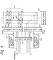
- Figure 5 is a block circuit diagram illustrating an EPROM device to which a high voltage detecting circuit is applied.
- the EPROM device has a plurality of terminals Ti - Tj being connected to an address buffer 51.
- the EPROM device has a function of selecting all word liens WL 1 - WL m and a function of selecting all bit lines BL 1 - BL n for testing all memory cells.
- the function of selecting all word lines is determined by a first specific mode signal applied to the terminal Ti
- the function of selecting all bit lines is determined by a second specific mode signal applied to the terminal Tj. Note, the first and second specific mode signals should not be applied to the terminal Ti and Tj at the same time.
- the prior high voltage detecting circuits 10a may generate an error control signal Soa without receiving the first specific mode signal, and at the same time, the prior high voltage detecting circuits 10b may generate an error control signal So b without receiving the second specific mode signal, for example, at the time the EPROM device is switched ON and the power line potential of the EPROM device is gradually increased, while the normal mode signal of the normal input voltage is continuously applied to the terminals T 1 and Tj of the EPROM device.
- a certain current flows in all of the memory cells of the EPROM device.
- a certain current e.g., about I ⁇ A
- the current flowing in the EPROM device is 64 mA
- the current flowing the EPROM device is about 260 mA.
- peripheral circuits, i.e., power supply 54, of the EPROM device cannot supply such large currents.
- a power line potential cannot be increased to the normal potential, and the power line potential remains at a certain value under the normal power line potential.
- the normal mode signal of the normal input voltage is continuously considered to be the specific mode signal higher by the predetermined value than the power line potential. Consequently, the flowing of the large current in the EPROM device is continued, until the EPROM device is destroyed.
- FIG. 6 is a block diagram illustrating a semiconductor memory device having an error checking and correction (ECC) circuit to which a high voltage detecting circuit is applied.
- the ECC circuit has a switching means S 1 - S 7 and a register 68 for setting signals in order to control the switching of the switching means by a latch control signal.
- Q normal mode for normal operation with correcting the error
- 02 a testing mode for testing information bits
- 0 a testing mode for testing inspection bits As a result of the above three modes, the information bits and the inspection bits can be tested independently without the normal operation mode.
- the register 68 is controlled by the output signal So c of the high voltage detecting circuit 10. That is, when the high voltage detecting circuit 10 generates a control signal for the testing mode of the ECC circuit, the ECC circuit changes to the testing mode for testing information bits or the testing mode for testing inspection bits from the normal mode for normal operation with correcting the error.
- the prior high voltage detecting circuits may generates an error control signal without receiving the specific mode signal, when the semiconductor memory device having the ECC circuit is switched ON and the power line potential of the device is gradually increased. Then the ECC circuit may change to the testing mode for testing information bits or the testing mode for testing inspection bits form the normal mode for normal operation with correcting the error, by the error control signal.
- Figure 7 is a block diagram illustrating a high voltage detecting circuit explaining a general concept of the present invention.
- a high voltage detecting circuit of the present invention is included in a semiconductor device having terminals 2, for generating a control signal So in order to start a specific mode of the semiconductor device when a potential of a specific mode signal higher by a predetermined value than a normal input voltage having a predetermined range is applied to at least one of the terminals 2 of the semiconductor device.
- the high voltage detecting circuit includes a first power supply means 7, a second power supply means 8, a blocking transistor 3, a level shift means 4, a resistor means 6, and a discrimination circuit 5.
- the first power supply means 7 is used for a high potential and the second power supply means 8 is used for a low potential.
- the blocking transistor 3 has a control electrode and two other electrodes, the control electrode being operatively connected to at least one of the terminals 2 of the semiconductor device and one of the two other electrodes being operatively connected to the first power supply means 7, for switching ON the blocking transistor 3 when a potential of the control electrode is higher than a potential of the one of the two other electrodes 2 by a threshold voltage of the blocking transistor 3.
- the level shift means 4 has an input end and an output end, the input end being operatively connected to the other of the two other electrodes of the blocking transistor 3 for obtaining a potential of the output end lower by a level shift value than a potential of the input end.
- the resistor means 6 has a first end and a second end, the first end being operatively connected to the output end of the level shift means 4, and the second end being operatively connected to the second power supply means 8, for keeping the potential of the first end to the low potential of the second power supply means 8 when a potential of at least one of the terminals 2 of the semiconductor device is within the predetermined range of the normal input voltage.
- the discrimination circuit 5 has a first end and a second end, the first end of the discrimination circuit 5 being operatively connected to the output end of the level shift means 4 and to the first end of the resistor means 6, for outputting the control signal So to the second end of the discrimination circuit 5, when a potential of the first end of the discrimination circuit 5 is higher than a threshold voltage of the discrimination circuit 5.
- FIG. 8 is a circuit diagram of a preferred embodiment of a high voltage detecting circuit according to the present invention.
- the high voltage detecting circuit is included in the semiconductor device as in the above description.
- a specific mode signal e.g., 8 volts
- a normal input voltage having a predetermined range e.g., from 0 volt to 5 volts
- a source of leakage current cutting off transistor Q ⁇ which is a P type MIS transistor, is connected to a terminal 2 of the semiconductor device.
- a gate and a drain of the transistor Q 1 are connected commonly to a source of a blocking transistor Qs , which is a P type MIS transistor.
- the leakage current cutting off transistor Qi is for keeping a leakage current under a predetermined standard current of the semiconductor device. Therefore, a potential of the source of the transistor Q 3 is lower by the threshold voltage of the transistor Qi than a potential of the terminal 2.
- a gate of the blocking transistor Q 3 is connected to a power line Vcc and a drain of the transistor Q s connected to an input end of a level shift circuit 4.
- the level shift circuit 4 includes k pieces of MIS transistors 0 41 , ..., Q 4k .
- a gate and a drain of the transistor Q 41 is commonly connected to the drain of the blocking transistor Q 3 as the input end of the level shift circuit 4.
- a source of the first transistor Q 41 is connected to a gate and a drain of a second transistor of the level shift circuit 4, and a source of the second transistor is connected to a gate and a drain of a third transistor of the level shift circuit 4 as same as the first transistor Q 41 .
- a source of a final transistor Q 4k is connected as the input end of the level shift circuit 4 to a drain of a resistor transistor Q 6 and to a first end of a discrimination circuit 5.
- the level shift circuit 4 is used for obtaining a potential of the output lower by a level shift value than a potential of the input end.
- the level shift value is determined by a sum of the threshold voltage of the k pieces of MIS transistors Q 41 , ..., Q 4k in the level shift circuit 4.
- the discrimination circuit 5 includes a first inverter circuit 5a and a second inverter circuit 5b, the first inverter circuit 5a consists of a P type MIS transistor Q 51 and an N type MIS transistor Q 52 , and the second inverter circuit 5b consists of a P type MIS transistor Q 53 and an N type MIS transistor Q 54 .
- the first end of a discrimination circuit 5, which is a common gate of a first inverter circuit 5a is connected to the output end of the level shift circuit 4 and to the drain of a resistor transistor Qs.
- the discrimination circuit 5 is for outputting the control signal So in order to start the specific mode of the semiconductor device to a second end of the discrimination circuit 5, which is a common drain of the inverter circuit 5b.
- the discrimination circuit 5 generates the control signal So, when a potential of the common gate of the first inverter circuit 5a is higher than the threshold voltage of the first inverter circuit 5a.
- the second inverter circuit 5b is for completing and inverting the output signal of the first inverter circuit 5a, sources of the transistor Q 51 and Q 53 are connected to the power line Vcc, and source of the transistor Q 52 and Qs4 are connected to the ground GND.
- the resistor Q 6 is a depletion type MIS transistor, and a gate and a source of the transistor Q 6 is commonly connected to the ground GND.
- the resistor transistor Q 6 is for keeping the potential of the drain of the transistor Q 6 to the low potential of the ground GND, when a potential of the terminal 2 of the semiconductor device is within the predetermined range of the normal input voltage. That is, the resistor transistor Q 6 flows an unnecessary electrical charge at the input end of the discrimination circuit 5 to the ground GND, when the potential of the input end changes from the high level to the low level.
- the operation of the high voltage detecting circuit will be described when the power line potential Vcc of the semiconductor device is stabilized, e.g., 5 volts.
- the normal mode operation of the semiconductor device will be described.
- the semiconductor device including the high voltage detecting circuit is used as the normal mode operation, that is, the normal mode signal within the predetermined range of the normal input voltage, e.g., 0-5 volts, which is not higher than the power line potential Vcc of 5 volts, supplied by another device, is applied to the terminal 2 of the semiconductor device.
- the potential of the input signal of the terminal 2 is dropped to the threshold voltage of the transistor Qi by cutting off the leakage current to transistor Qi and applying it to the source of the blocking transistor Qa.
- the blocking transistor Q 3 is switched OFF, since the transistor Q 3 is switched ON only when the potential of the source of the transistor Q 3 is higher by the threshold voltage of the transistor Q 3 , than the potential of the gate of the transistor Q 3 which is power line potential Vcc. Therefore, the input end of the level shift circuit 4 is at the low level and the common gate of the first inverter circuit 5a is also at the low level, and thus the common drain of the second inverter circuit 5b is at the low level. This is, when the power line potential Vcc is stabilized while the normal mode signal is applied to the terminal 2, the high voltage detecting circuit will not generate the control signal So for starting the specific mode of the semiconductor device.
- the specific mode operation of the semiconductor device When the semiconductor device including the high voltage detecting circuit is used as the specific mode operation, e.g., testing mode operation. That is, the specific mode signal, e.g., 8 volts, higher by the predetermined value than the normal input voltage, is applied to the terminal 2 of the semiconductor device.
- the potential of the source of the transistor Q 3 is higher by the threshold voltage of the transistor Q 3 than the potential of the gate of the transistor Qs , but the potential of the input signal of the terminal 2 is dropped to the threshold voltage of the transistor Q 1 by cutting off the leakage current at the transistor Q 1 and applying it to the source of the blocking transistor Qs.
- the blocking transistor Q 3 is switched ON and the input end of the level shift circuit 4 is at the high level.
- the potential of the input end of the level shift circuit 4 is dropped to the sum of the threshold voltages of k pieces of MIS transistors Q 41 , ..., Q 4k in the level shift circuit 4 by the transistors Q 41 , ..., Q 4k , which is the threshold voltage of the level shift circuit 4, the output end of the level shift circuit 4 is still at the high level. That is, the potential of the output of the level shift circuit 4 is higher than the threshold voltage of the first inverter circuit 5a, and the potential of the specific mode signal is determined by the threshold voltages of the transistors Qi and Q 3 , the level shift circuit 4, and the first inverter circuit 5a.
- the common gate of the first inverter circuit 5a is at the high level, and thus the common drain of the second inverter circuit is at the high level. That is, when the power line potential Vcc is stabilized and the specific mode signal is applied to the terminal 2, the high voltage detecting circuit generates the control signal So for starting the specific mode of the semiconductor device.
- the operation of the high voltage detecting circuit will be described when the power line potential Vcc of the semiconductor device is not stabilized, e.g., when the semiconductor device is switched ON.
- Figure 9 is a graph illustrating the high voltage detecting circuit shown in Fig. 8 at the time of switching ON the semiconductor device.
- the semiconductor device including the high voltage detecting circuit When the semiconductor device including the high voltage detecting circuit is switched ON at a time to , the power line potential Vcc is gradually increased from the time to to a time t 3 until the power line potential is stabilized, a shown by a line a in Fig. 9.
- the normal mode signal of the normal input voltage is continuously applied to the terminal of the semiconductor device, shown by a line b in Fig. 9, and at the same time the semiconductor device is switched ON, the normal mode signal having the potential of the line b is considered to be the specific mode signal.
- the blocking transistor Q 3 is switched ON from the time to to a time t 2 , that is, the blocking transistor Q 3 is switched ON until the time that the normal mode signal is not considered to be the specific mode signal.
- the blocking transistor Q 3 is switched ON.
- the inverter circuits 5a and 5b cannot be operated until the power line potential exceeds an operable voltage V 1 of the inverter circuits. Consequently, it is possible to generate an error control signal for starting the specific mode of the semiconductor device from a time ti to the time t 2 in the high voltage detecting circuit. But in the high voltage detecting circuit shown in Fig.
- the potential of the drain of the blocking transistor is dropped the predetermined value by the level shift circuit 4, and the potential of the common gate of the first inverter circuit 5a is not higher than the threshold voltage of the inverter circuit 5a (i.e., the threshold voltage of the transistor Q 51 of the first inverter circuit 5a). Consequently, the error control signal for starting the specific mode of the semiconductor device is not generated, even if the potential of the source of the blocking transistor Q 3 is higher by the threshold voltages of the transistor Q 3 than the increasing power line potential.
- the predetermined voltage value of the level shift circuit 4 is indicated by a reference mark a
- the threshold voltages of the transistors Q 1 and Q 3 are indicated by reference marks Vthi and Vth 3 respectively
- the threshold voltage of the transistor Q 51 of the first inverter circuit 5a is indicated by a reference mark Vthsi
- the increasing power line voltage is indicated by a reference mark Vx
- the potential of the input end of the first inverter circuit 5a is indicated by a reference mark V G
- the potential of the normal input signal is indicated by a reference mark Vo.
- the potential of the normal input signal applied to the terminal 2 is Vo , e.g., 5 volts, and the potential V G is indicated by the following formula.
- the potential Vx being applied to the source of blocking transistor Q 3 is higher by the threshold voltage Vth 51 of the transistor Q 51 than the potential V G being applied to the gate of blocking transistor 0 3 . Therefore the potential V G is indicated by the following formula.
- the predetermined voltage value a is indicated by the following formula.
- the possibility of generating the error control signal is in a range of V 1 ⁇ V X ⁇ V 2 , and the predetermined voltage value a is indicated by the following formula.
- the predetermined voltage value a, dropped by the level shift circuit 4 be determined as satisfying the above formula (D).
- the value a is determined by the formula (D)
- the potential of the output of the level shift circuit 4 is not higher than the threshold voltage of the first inverter circuit 5a, even when the semiconductor device is switched ON while the normal mode signal of the normal input voltage is continuously applied to the terminal of the semiconductor device.
- the potential V G of the input end of the first inverter circuit 5a is not higher than the threshold voltage Vthsi of the transistor Q 51 in the first inverter circuit 5a, the P type MIS transistor Q 51 is switched ON and the transistor Q 52 is switched OFF. Therefore, the potential of the output end of the first inverter 5a is at the high level and the potential of the output end of the second inverter 5b is at the low level, that is the control signal So is not generated.
- the potential V G of the input end of the first inverter circuit 5a should be at the high level, e.g., the potential Vo of the normal input signal, when the potential ⁇ of the specific mode signal is applied to the terminal of the semiconductor device.
- the normal input signal V o is equal to the power line potential Vcc when the semiconductor device is stabilized, and therefore, the potential V G of the input end of the first inverter circuit 5a is indicated by the following formula.
- the potential of the specific mode signal should be determined in accordance with the voltage value a of dropped by the level shift circuit 4 as shown in the formula (Co). That is, if the predetermined voltage value a is established as the higher value, the potential should be determined as the higher value. Consequently, the predetermined voltage value a should not be established as the higher value unless absolutely necessary.
- FIG. 4 is a block circuit diagram illustrating a latch circuit to which a high voltage detecting circuit is applied.
- the latch circuit included in a certain semiconductor device (not shown), e.g., semiconductor memory device, has three terminals 2a, 2b, and 2c, a logic circuit 40, and a high voltage detecting circuit 10.
- the terminal 2a is connected to an internal circuit of the semiconductor device, and the terminal 2a is also connected to a high voltage detecting circuit 10.
- the terminal 2b is connected through a buffer B 1 to the logic circuit 40 and through a buffer B 2 to the internal circuit of the semiconductor device.
- the terminal 2c is connected through a buffer B 3 to the logic circuit 40 and to the internal circuit of the semiconductor device.
- a signal of the terminal 2a is transmitted to the internal circuit directly, as shown by reference marks D 1
- signals of the terminal 2b and 2c are transmitted to the internal circuit through the buffer B 2 and B 3 respectively, as shown by reference marks D 2 and D 4 .
- each potential of the signal D 1 , D 2 , and D 4 is within a normal input voltage and a power line potential is stabilized.
- the high voltage detecting circuit 10 does not generate a control signal So , that is, an output signal of the high voltage detecting circuit 10 is at a low level.
- a control signal So for starting a specific mode of the semiconductor device is generated from the high voltage detecting circuit 10. While the control signal, which is at a high level, is generated from the high voltage detecting circuit 10, at the same time, a high level signal within a normal input voltage is applied to the terminal 2b, an output signal of an NAND gate NG 2 is at the low level and an output signal of an NAND gate NG 1 is at the high level. Therefore, an output signal of an NAND gate NG 4 is at the high level and an output signal of an NAND gate NG 3 is at the low level.
- the output signal of the NAND gate NG 3 is at the low level. Therefore, an output signal of an NAND gate NG 5 is at the high level as shown by a reference mark D 3 and the output signal of the NAND gate NGs which is at the high level is applied to the internal circuit.
- the output signal D 3 of the NAND gate NGs is continuously at the high level without applying a specific mode signal to the terminal 2a.
- FIG. 5 is a block circuit diagram illustrating an EPROM device to which a high voltage detecting circuit is applied.
- the EPROM device has a function of selecting all word lines WL 1 - WLm and a function of selecting all bit lines BL 1 - BL n for testing all memory cells.
- the EPROM device has a plurality of terminals Ti - Tj connected to an address buffer 51.
- the terminal T 1 of the terminals T 1 - Tj are connected to a high voltage detecting circuit 10a and an output 9a of the high voltage detecting circuit 10a is applied to a word line decoder 52.
- the terminal Tj of the terminals Ti - Tj is connected to a high voltage detecting circuit 10b and an output 9b of the high voltage detecting circuit 10b is applied to a bit line decoder 53.
- the word line decoder 52 has a plurality of word lines WL i - WL m , the bit line decoder 53 many bit lines BL 1 - BL n , and there are a plurality of memory cells MC at each cross point of the word lines WL 1 - WLmand the bit lines BL 1 - BL n .
- the function of selecting all word lines and the function of selecting all bit lines are used to give stress to the memory cells, and thereby test them.
- the function of selecting all word lines is determined by a first specific mode signal applied to the terminals Ti , and the function of selecting all bit lines is determined by a second specific mode signal applied to the terminal Tj. Note, the first and second specific mode signals should not be applied to the terminals Ti and Tj , at the same time.
- reference numeral 54 denotes a power supply.
- a signal of each terminal Ti Tj is transmitted to the word line decoder 52 and the bit line decoder 53 through the address buffer 51.
- normal address signals within a normal input voltage are applied to the terminals Ti - Tj , and the high voltage detecting circuits 10a and 10b do not generate starting signals Soa and Sob , respectively.
- the first specific signal or the second specific signal is applied to the terminals T 1 - Tj , and then one of the high voltage detecting circuits 10a and 10b generates a control signal Soaor Sob. In this case, the high voltage detecting circuits 10a and 10b should not generate a control signal at the same time.
- FIG. 6 is a block circuit diagram illustrating a semiconductor memory device having an error checking and correction (ECC) circuit to which a high voltage detecting circuit is applied.
- the ECC circuit has a switching means Si - S 7 and a register 68 for setting signals in order to control the switching of the switching means by a latch control signal.
- 1 a normal mode for normal operation with correcting the error
- 2 a testing mode for testing information bits
- 3 a testing mode for testing inspection bits.
- reference normal 10 denotes a high voltage detecting circuit (HD)
- reference numeral 61 denotes data input (Din)
- reference numeral 62 denotes a plurality of address input (Ain)
- a reference numeral 63 denotes a encorder (COD)
- reference numeral 64 denotes information bits (IB)
- reference numeral 65 denotes inspection bits (PB)
- reference numeral 66 denotes a decoder (DEC)
- reference numeral 67 denotes an error checking and correction circuit having data output (Do)
- reference numeral 68 denotes a register.
- the switching of the switching means is controlled by the register 68, which is provided with predetermined information of the switching state of the above three modes.
- the semiconductor circuits using the embodiments of the high voltage detecting circuit according to the present invention are not started in testing mode by the error control signal for starting the testing mode of the semiconductor circuit generated from the high voltage detecting circuit.
Abstract
Description
- The present invention relates to a high voltage detecting circuit, and in particular, to a high voltage detecting circuit included in a semiconductor device having terminals, for generating a control signal to start a specific operating mode of the semiconductor device, when the potential of a specific mode signal higher by a predetermined value then a normal input voltage having a predetermined range, is applied to at least one of the terminals of the semiconductor device.
- In general, a high voltage detecting circuit is included in a semiconductor device for detecting a potential of a terminal of the semiconductor device. When the potential of the terminal of the device is higher by a predetermined value than a normal input voltage having a predetermined range, the high voltage detecting circuit generates a control signal for starting a specific mode of the semiconductor device. Upon receiving the control signal, the semiconductor device changes to the specific mode, e.g., a testing mode. Such a high voltage detecting circuit is disclosed in, for example, JP-A-60-124124 and comprises
- a first power supply means for a high potential;
- a second power supply means for a low potential;
- a blocking transistor, having a control electrode and two other electrodes, the control electrode being coupled to the at least one of the terminals and, one of the two other electrodes being connected to the first power supply means, the blocking transistor switching ON when the potential of the control electrode is higher by the threshold voltage of the blocking transistor than the potential of the one of the two other electrodes; and
- a discrimination circuit, having a first end and a second end, the first end of the discrimination circuit being coupled to the other of the two other electrodes of the blocking transistor for outputting the control signal from the second end of the discrimination circuit when the potential of the first end of the discrimination circuit is higher than a threshold voltage of the discrimination circuit by virtue of the blocking transistor being turned ON.
- When a potential of a power line (hereinafter referred to as a power line potential) of the semiconductor device is stable the prior high voltage detecting circuit, as in JP-A-60-124124 generates or does not generate the control signal exactly in accordance with the potential applied from an another device to the terminal of the semiconductor device. That is, when the potential of the terminal of the semiconductor device is within the predetermined range of the normal input voltage, the prior high voltage detecting circuit does not generate the control signal for starting the specific mode of the device. However, when the potential of the terminal or the semiconductor device is higher by the predetermined value than the normal input voltage, the prior high voltage detecting circuit generates the control signal and the semiconductor device changes to the specific mode, e.g., to the testing mode.
- When, however, the power line potential of the semiconductor device is not stable, for example, immediately after the semiconductor device is switched ON, and so when the power line potential of the device gradually increases, while the normal mode signal of the normal input voltage is continuously applied to the terminal of the semiconductor device: the normal mode signal of the terminal of the semiconductor device may be higher by the predetermined value than the increased power line potential. That is, the normal signal of the normal input voltage is considered to be the control signal for starting the specific mode of the semiconductor device. Consequently, the prior high voltage detecting circuit may generate a control signal in error without receiving the specific mode signal, and the semiconductor device may be changed to the specific mode by the erroneous control signal.
- According to the this invention, such a high voltage detecting circuit includes level shift means having an input end and an output end, the input end being connected to the other of the two other electrodes of the blocking transistor, the level shift means obtaining a potential at the output end lower by a level shifted value than the potential at its input end; and,
- resistor means, having a first end and a second end, the first end being connected to the output end of the level shift means and the second end being connected to the second power supply means, the first end of the discrimination circuit being connected to the output end of the level shift means and to the first end of the resistor means;
- the resistor means keeping the potential of the first end at the low potential of the second power supply means when the potential of the at least one of the terminals is within the predetermined range of the normal input voltage.
- The level shift means may include at least one MIS transistor, having a control electrode and two other electrodes. The control electrode is operatively connected to one of the two other electrodes. The other of the two other electrodes is operatively connected to the first end of the resistor means. The level shift value is determined by the threshold voltage of at lest one MIS transistor.
- The resistor means may include a depletion type MIS transistor, having a control electrode and two other electrodes. The control electrode is operatively connected to one of the two other electrodes and to the second power supply means. The other of the two other electrodes is operatively connected to at least one of the terminals of the semiconductor device, for keeping a leakage current under a predetermined standard current of the semiconductor device.
- The present invention will now be described and contrasted with the prior art with reference to the accompanying drawings, wherein:-
- Figure I is a block diagram illustrating a semiconductor device including a high voltage detecting circuit;
- Fig. 2 is a circuit diagram of an example of a conventional high voltage detecting circuit;
- Fig. 3 is a graph illustrating the conventional high voltage detecting circuit shown in Fig. 2 at the time switching ON the semiconductor device;
- Fig. 4 is a block circuit diagram illustrating a latch circuit to which a high voltage detecting circuit is applied;
- Fig. 5 is a block circuit diagram illustrating an EPROM device to which a high voltage detecting circuit is applied;
- Fig 6 is a block circuit diagram illustrating a semiconductor memory device having an ECC circuit to which a high voltage detecting circuit is applied;
- Fig. 7 is a block diagram illustrating a high voltage detecting circuit explaining a general concept of the present invention;
- Fig. 8 is a circuit diagram of a preferred embodiment of a high voltage detecting circuit according to the present invention; and
- Fig. 9 is a graph illustrating the high voltage detecting circuit shown in Fig. 8 at the time of switching ON the semiconductor device.
- For a better understanding of the preferred embodiments, the problems in the related art will be first explained.
- Figure I is a block diagram illustrating a semiconductor device including a high voltage detecting circuit. As shown in Fig. I, a
terminal 32 of asemiconductor device 30 is connected to aninternal circuit 35 and a signal of theterminal 32 is transmitted directly to theinternal circuit 35. Theterminal 32 is also connected to a highvoltage detecting circuit 31. When a potential of a specific mode signal higher by a predetermined value than a normal voltage having a predetermined range is applied to theterminal 32 of thesemiconductor device 30, the highvoltage detecting circuit 31 generates a control signal. The control signal is transmitted to aspecific mode circuit 33, and thespecific mode circuit 33 makes theinternal circuit 35, to a specific mode. That is, when the specific mode signal is applied to theterminal 32 of thesemiconductor device 30, thesemiconductor device 30 changes to the specific mode, e.g., a testing mode. - Figure 2 is a circuit diagram of an example of a conventional high voltage detecting circuit. The high voltage detecting circuit is included in a semiconductor device as in the above description with reference to Fig. I. When a specific mode signal, e.g., 8 volts, higher by a predetermined value than a normal input voltage having a predetermined range, e.g., from 0 volt to 5 volts, is applied to a
terminal 12 of the semiconductor device, the high voltage detecting circuit generates a control signal S01 for starting a specific mode of the semiconductor device. - A source of a leakage current cutting off transistor Q11 , which is a P-channel type MIS transistor, is connected to the
terminal 12 of the semiconductor device, and a gate and drain of the transistor Q11 are connected commonly to a source of a P type MIS transistor Q13. A gate and a drain of the transistor Q13 are connected to a gate and a drain of an N-channel type MIS transistor Qi4, respectively, and a source of the transistor Q14 is connected to a ground GND. A common gate of both transistors Q13 and Q14 is connected to a power line Vcc (the reference mark Vcc also indicates a power line potential). A common drain of both transistors Q13 and Q14 is connected to a common gate of afirst inverter circuit 15 consisting of a P type M18 transistor Q151 and an N type MIS transistor Q152. A common drain of thefirst inverter circuit 15 is connected to a common gate of asecond inverter circuit 16 consisting of a P type MIS transistor Q161 and an N type MIS transistor Q162. A common drain of thesecond inverter circuit 16 is anoutput end 19 of the high voltage detecting circuit and the control signal S01 is transmitted from theoutput end 19 to the internal circuit through the specific mode circuit of the semiconductor device. In the above description, sources of the transistor Q151 and Q161 are connected to the power line Vcc and sources of the transistor Q152 and Q162 are connected to the ground GND. - In the above high voltage detecting circuit, when the power line potential Vcc is stabilized, e.g., 5 volts, and a normal mode signal within the normal input voltage, e.g., from 0 volt to 5 volts, is applied to the
terminal 12, the high voltage detecting circuit does not generate the control signal. Because a potential of the source of the transistor Q13 is not higher by the threshold voltage of the transistor Q13 than a potential of the gate of the transistor 013, the transistor Qi3 is not switched ON. Consequently, a potential of the common gate of thefirst inverter circuit 15 is at a low level, a potential of the common gate of thesecond inverter circuit 16 is at a high level, and theoutput end 19 of the high voltage detecting circuit is at the low level. That is, the control signal S01 is not generated and the semiconductor device continues in a normal mode operation. - When the power line potential Vcc is stabilized, e.g., 5 volts, and the specific mode signal, e.g., 8 volts, higher by a predetermined value than the normal input voltage is applied to the
terminal 12, the high voltage detecting circuit generates the control signal. Because a potential of the source of the transistor Q13 is higher by the threshold voltage of the transistor Q13 than a potential of the gate of the transistor Q13 , the transistor Q13 is switched ON. Consequently, a potential of the common gate of thefirst inverter circuit 15 is at the high level, a potential of the common gate of thesecond inverter circuit 16 is at the low level, and theoutput end 19 of the high voltage detecting circuit is at the high level. That is, the staring signal S01 is generated and the semiconductor device changes to the specific mode operation. - Figure 3 is a graph illustrating the conventional high voltage detecting circuit shown in Fig. 2 at the time of switching ON the semiconductor device.
- In Fig. 3, when the power line potential Vcc is stabilized at a time t14 in Fig. 3 of a potential Vio (e.g., 5 volts), and the specific mode signal, shown by a line c1 in Fig. 3, of a potential V13 (e.g., 8 volts) higher by the predetermined value than the normal input voltage under a potential V10, is applied to the
terminal 12 of the semiconductor device, the high voltage detecting circuit generates the control signal S01. - When the semiconductor device including the high voltage detecting circuit is switched ON at a time tio , the power line potential Vcc is gradually increased from 0 volt at the time t10 to the stabilized power line potential V10 (e.g., 5 volts) at a time t13, shown by a line a1 in Fig. 3, until the power line potential Vcc is stabilized. At the same time, the normal mode signal of the normal input voltage (e.g., under 5 volts( is continuously applied to the terminal of the semiconductor device, shown by a line bi in Fig. 3, and the high voltage detecting circuit may generate an error control signal for starting the specific mode of the semiconductor device, because when the semiconductor device is switched ON and the power line potential Vcc of the device is gradually increased, the normal mode signal of the normal input voltage is considered to be the staring signal higher by the predetermined value than the increased power line potential a1 below a potential V12 at a time t12. In Fig. 3, a potential V11 at a time t11 is an operational potential of the device, that is, the potential V11 is an operational potential of the inverter circuit of the device. Therefore, the high voltage detecting circuit may generate the error control signal from the time t11 to the time t12 , when the semiconductor device is switched ON and a power line potential of the device is gradually increased, while the potential of the terminal of the semiconductor device is within a normal input voltage having a predetermined range.
- Next, problems of semiconductor circuits using the above prior high voltage detecting circuit will be described with reference to Figs. 4, 5, and 6.
- Figure 4 is a block circuit diagram illustrating a latch circuit to which a high voltage detecting circuit is applied. In Fig. 4, the latch circuit is included in a semiconductor device (not shown), e.g., semiconductor memory device. The latch circuit is useful for setting the semiconductor device to a specific mode continuously, without a specific mode signal being continuously applied to a terminal 2a. A signal of the terminal 2a is transmitted to the internal circuit directly, as shown by reference marks D1. Signals of the terminals 2b and 2c are transmitted to the internal circuit through the buffers B2 and B3 respectively, as shown by reference marks D2 and D4. That is, the semiconductor device changes to the specific mode and continues the specific mode by one time receipt of the specific signal, and therefore, all
terminals 2a, 2b and 2c can be used as input terminals at the specific mode. In the case of a normal mode operation of the semiconductor device, an output signal D3 of a NAND gate NG5 can be changed to a low level or a high level in accordance with a signal of the terminal 2c. On the other hand, in the specific mode operation of the semiconductor device, the output signal D3 of the NAND gate NGs is fixed at the high level independently of the signal of the terminal 2c. That is, the semiconductor device is fixed to the specific mode, e.g., a testing mode, by the high level signal D3. In the above description, the testing mode is for testing the semiconductor device before forwarding the semiconductor device from a production factory. - The prior high voltage detecting circuit may generate an error control signal without receiving the specific mode signal, for example, the semiconductor device is switched ON and the power line potential of the device is gradually increased while the normal mode signal of the normal input voltage is continuously applied to the terminal of the semiconductor device. Consequently, the latch circuit being applied the prior high voltage detecting circuit, may continuously generate the control signal for staring the specific mode of the semiconductor device without the specific signal being continuously applied to a terminal of the semiconductor device.
- Figure 5 is a block circuit diagram illustrating an EPROM device to which a high voltage detecting circuit is applied. In Fig. 5, the EPROM device has a plurality of terminals Ti - Tj being connected to an
address buffer 51. The EPROM device has a function of selecting all word liens WL1 - WLm and a function of selecting all bit lines BL1 - BLn for testing all memory cells. The function of selecting all word lines is determined by a first specific mode signal applied to the terminal Ti , and the function of selecting all bit lines is determined by a second specific mode signal applied to the terminal Tj. Note, the first and second specific mode signals should not be applied to the terminal Ti and Tj at the same time. - However, the prior high
voltage detecting circuits 10a may generate an error control signal Soa without receiving the first specific mode signal, and at the same time, the prior highvoltage detecting circuits 10b may generate an error control signal Sobwithout receiving the second specific mode signal, for example, at the time the EPROM device is switched ON and the power line potential of the EPROM device is gradually increased, while the normal mode signal of the normal input voltage is continuously applied to the terminals T1 and Tj of the EPROM device. When the highvoltage detecting circuits power supply 54, of the EPROM device cannot supply such large currents. Thus, a power line potential cannot be increased to the normal potential, and the power line potential remains at a certain value under the normal power line potential. When the power line potential remains at a certain value, the normal mode signal of the normal input voltage is continuously considered to be the specific mode signal higher by the predetermined value than the power line potential. Consequently, the flowing of the large current in the EPROM device is continued, until the EPROM device is destroyed. - Figure 6 is a block diagram illustrating a semiconductor memory device having an error checking and correction (ECC) circuit to which a high voltage detecting circuit is applied. In Fig. 6, the ECC circuit has a switching means S1 - S7 and a
register 68 for setting signals in order to control the switching of the switching means by a latch control signal. There are three modes in the semiconductor memory device having the ECC circuit in accordance with a state of theregister 68, as follows; Q a normal mode for normal operation with correcting the error, 02 a testing mode for testing information bits, and 0 a testing mode for testing inspection bits. As a result of the above three modes, the information bits and the inspection bits can be tested independently without the normal operation mode. Theregister 68 is controlled by the output signal Soc of the highvoltage detecting circuit 10. That is, when the highvoltage detecting circuit 10 generates a control signal for the testing mode of the ECC circuit, the ECC circuit changes to the testing mode for testing information bits or the testing mode for testing inspection bits from the normal mode for normal operation with correcting the error. - But the prior high voltage detecting circuits may generates an error control signal without receiving the specific mode signal, when the semiconductor memory device having the ECC circuit is switched ON and the power line potential of the device is gradually increased. Then the ECC circuit may change to the testing mode for testing information bits or the testing mode for testing inspection bits form the normal mode for normal operation with correcting the error, by the error control signal.
- Referring to Figs. 7,8 and 9, the preferred embodiments according to the present invention will be described.
- Figure 7 is a block diagram illustrating a high voltage detecting circuit explaining a general concept of the present invention.
- As shown in Fig. 7, a high voltage detecting circuit of the present invention is included in a semiconductor
device having terminals 2, for generating a control signal So in order to start a specific mode of the semiconductor device when a potential of a specific mode signal higher by a predetermined value than a normal input voltage having a predetermined range is applied to at least one of theterminals 2 of the semiconductor device. - The high voltage detecting circuit includes a first power supply means 7, a second power supply means 8, a blocking
transistor 3, a level shift means 4, a resistor means 6, and adiscrimination circuit 5. The first power supply means 7 is used for a high potential and the second power supply means 8 is used for a low potential. The blockingtransistor 3 has a control electrode and two other electrodes, the control electrode being operatively connected to at least one of theterminals 2 of the semiconductor device and one of the two other electrodes being operatively connected to the first power supply means 7, for switching ON the blockingtransistor 3 when a potential of the control electrode is higher than a potential of the one of the twoother electrodes 2 by a threshold voltage of the blockingtransistor 3. - The level shift means 4 has an input end and an output end, the input end being operatively connected to the other of the two other electrodes of the blocking
transistor 3 for obtaining a potential of the output end lower by a level shift value than a potential of the input end. The resistor means 6 has a first end and a second end, the first end being operatively connected to the output end of the level shift means 4, and the second end being operatively connected to the second power supply means 8, for keeping the potential of the first end to the low potential of the second power supply means 8 when a potential of at least one of theterminals 2 of the semiconductor device is within the predetermined range of the normal input voltage. Thediscrimination circuit 5 has a first end and a second end, the first end of thediscrimination circuit 5 being operatively connected to the output end of the level shift means 4 and to the first end of the resistor means 6, for outputting the control signal So to the second end of thediscrimination circuit 5, when a potential of the first end of thediscrimination circuit 5 is higher than a threshold voltage of thediscrimination circuit 5. - Figure 8 is a circuit diagram of a preferred embodiment of a high voltage detecting circuit according to the present invention. The high voltage detecting circuit is included in the semiconductor device as in the above description. When a specific mode signal, e.g., 8 volts, higher by a predetermined value than a normal input voltage having a predetermined range, e.g., from 0 volt to 5 volts, is applied to the
terminal 2 of the semiconductor device, the high voltage detecting circuit generates a control signal So for starting a specific mode of the semiconductor device. - A source of leakage current cutting off transistor Q↑ , which is a P type MIS transistor, is connected to a
terminal 2 of the semiconductor device. A gate and a drain of the transistor Q1 are connected commonly to a source of a blocking transistor Qs , which is a P type MIS transistor. The leakage current cutting off transistor Qi is for keeping a leakage current under a predetermined standard current of the semiconductor device. Therefore, a potential of the source of the transistor Q3 is lower by the threshold voltage of the transistor Qi than a potential of theterminal 2. - A gate of the blocking transistor Q3 is connected to a power line Vcc and a drain of the transistor Qs connected to an input end of a
level shift circuit 4. When a potential of the gate of the transistor Q3 is higher by the threshold voltage of the blocking transistor Q3 than a potential of the source of the transistor Q3 , the blocking transistor Q3 is switched ON. - The
level shift circuit 4 includes k pieces of MIS transistors 041 , ..., Q4k. In a first transistor 041 of thelevel shift circuit 4, a gate and a drain of the transistor Q41 is commonly connected to the drain of the blocking transistor Q3 as the input end of thelevel shift circuit 4. A source of the first transistor Q41 is connected to a gate and a drain of a second transistor of thelevel shift circuit 4, and a source of the second transistor is connected to a gate and a drain of a third transistor of thelevel shift circuit 4 as same as the first transistor Q41. A source of a final transistor Q4k is connected as the input end of thelevel shift circuit 4 to a drain of a resistor transistor Q6 and to a first end of adiscrimination circuit 5. Thelevel shift circuit 4 is used for obtaining a potential of the output lower by a level shift value than a potential of the input end. The level shift value is determined by a sum of the threshold voltage of the k pieces of MIS transistors Q41 , ..., Q4k in thelevel shift circuit 4. - The
discrimination circuit 5 includes afirst inverter circuit 5a and asecond inverter circuit 5b, thefirst inverter circuit 5a consists of a P type MIS transistor Q51 and an N type MIS transistor Q52, and thesecond inverter circuit 5b consists of a P type MIS transistor Q53 and an N type MIS transistor Q54. The first end of adiscrimination circuit 5, which is a common gate of afirst inverter circuit 5a, is connected to the output end of thelevel shift circuit 4 and to the drain of a resistor transistor Qs. Thediscrimination circuit 5 is for outputting the control signal So in order to start the specific mode of the semiconductor device to a second end of thediscrimination circuit 5, which is a common drain of theinverter circuit 5b. That is, thediscrimination circuit 5 generates the control signal So, when a potential of the common gate of thefirst inverter circuit 5a is higher than the threshold voltage of thefirst inverter circuit 5a. In the above description, thesecond inverter circuit 5b is for completing and inverting the output signal of thefirst inverter circuit 5a, sources of the transistor Q51 and Q53 are connected to the power line Vcc, and source of the transistor Q52 and Qs4 are connected to the ground GND. - The resistor Q6 is a depletion type MIS transistor, and a gate and a source of the transistor Q6 is commonly connected to the ground GND. The resistor transistor Q6 is for keeping the potential of the drain of the transistor Q6 to the low potential of the ground GND, when a potential of the
terminal 2 of the semiconductor device is within the predetermined range of the normal input voltage. That is, the resistor transistor Q6 flows an unnecessary electrical charge at the input end of thediscrimination circuit 5 to the ground GND, when the potential of the input end changes from the high level to the low level. - Referring to Fig. 8, the operation of the high voltage detecting circuit will be described when the power line potential Vcc of the semiconductor device is stabilized, e.g., 5 volts.
- First, the normal mode operation of the semiconductor device will be described. When the semiconductor device including the high voltage detecting circuit is used as the normal mode operation, that is, the normal mode signal within the predetermined range of the normal input voltage, e.g., 0-5 volts, which is not higher than the power line potential Vcc of 5 volts, supplied by another device, is applied to the
terminal 2 of the semiconductor device. The potential of the input signal of theterminal 2 is dropped to the threshold voltage of the transistor Qi by cutting off the leakage current to transistor Qi and applying it to the source of the blocking transistor Qa. - Therefore, the blocking transistor Q3 is switched OFF, since the transistor Q3 is switched ON only when the potential of the source of the transistor Q3 is higher by the threshold voltage of the transistor Q3, than the potential of the gate of the transistor Q3 which is power line potential Vcc. Therefore, the input end of the
level shift circuit 4 is at the low level and the common gate of thefirst inverter circuit 5a is also at the low level, and thus the common drain of thesecond inverter circuit 5b is at the low level. This is, when the power line potential Vcc is stabilized while the normal mode signal is applied to theterminal 2, the high voltage detecting circuit will not generate the control signal So for starting the specific mode of the semiconductor device. - Next, the specific mode operation of the semiconductor device will be described. When the semiconductor device including the high voltage detecting circuit is used as the specific mode operation, e.g., testing mode operation. That is, the specific mode signal, e.g., 8 volts, higher by the predetermined value than the normal input voltage, is applied to the
terminal 2 of the semiconductor device. The potential of the source of the transistor Q3 is higher by the threshold voltage of the transistor Q3 than the potential of the gate of the transistor Qs , but the potential of the input signal of theterminal 2 is dropped to the threshold voltage of the transistor Q1 by cutting off the leakage current at the transistor Q1 and applying it to the source of the blocking transistor Qs. - Consequently, the blocking transistor Q3 is switched ON and the input end of the
level shift circuit 4 is at the high level. Although the potential of the input end of thelevel shift circuit 4 is dropped to the sum of the threshold voltages of k pieces of MIS transistors Q41 , ..., Q4k in thelevel shift circuit 4 by the transistors Q41 , ..., Q4k , which is the threshold voltage of thelevel shift circuit 4, the output end of thelevel shift circuit 4 is still at the high level. That is, the potential of the output of thelevel shift circuit 4 is higher than the threshold voltage of thefirst inverter circuit 5a, and the potential of the specific mode signal is determined by the threshold voltages of the transistors Qi and Q3, thelevel shift circuit 4, and thefirst inverter circuit 5a. Therefore, the common gate of thefirst inverter circuit 5a is at the high level, and thus the common drain of the second inverter circuit is at the high level. That is, when the power line potential Vcc is stabilized and the specific mode signal is applied to theterminal 2, the high voltage detecting circuit generates the control signal So for starting the specific mode of the semiconductor device. - Referring to Fig. 9, the operation of the high voltage detecting circuit will be described when the power line potential Vcc of the semiconductor device is not stabilized, e.g., when the semiconductor device is switched ON.
- Figure 9 is a graph illustrating the high voltage detecting circuit shown in Fig. 8 at the time of switching ON the semiconductor device.
- When the semiconductor device including the high voltage detecting circuit is switched ON at a time to , the power line potential Vcc is gradually increased from the time to to a time t3 until the power line potential is stabilized, a shown by a line a in Fig. 9. When the normal mode signal of the normal input voltage is continuously applied to the terminal of the semiconductor device, shown by a line b in Fig. 9, and at the same time the semiconductor device is switched ON, the normal mode signal having the potential of the line b is considered to be the specific mode signal. Because the potential of the source of the blocking transistor Q3 which has the potential lower by the threshold voltages of the transistor Q1 than the potential of the normal mode signal, is higher by the threshold voltages of the transistor Q3 than the potential of the gate of the transistor Q3 , which is the increasing power line potential of the line a. Therefore, the blocking transistor Q3 is switched ON from the time to to a time t2 , that is, the blocking transistor Q3 is switched ON until the time that the normal mode signal is not considered to be the specific mode signal.
- However, when the potential of the output end of the level shift circuit is at the low level, the blocking transistor Q3 is switched ON. Note, the
inverter circuits level shift circuit 4, and the potential of the common gate of thefirst inverter circuit 5a is not higher than the threshold voltage of theinverter circuit 5a (i.e., the threshold voltage of the transistor Q51 of thefirst inverter circuit 5a). Consequently, the error control signal for starting the specific mode of the semiconductor device is not generated, even if the potential of the source of the blocking transistor Q3 is higher by the threshold voltages of the transistor Q3 than the increasing power line potential. Note, the predetermined voltage value of thelevel shift circuit 4 is indicated by a reference mark a, the threshold voltages of the transistors Q1 and Q3 are indicated by reference marks Vthi and Vth3 respectively, the threshold voltage of the transistor Q51 of thefirst inverter circuit 5a is indicated by a reference mark Vthsi , the increasing power line voltage is indicated by a reference mark Vx , the potential of the input end of thefirst inverter circuit 5a is indicated by a reference mark VG , and the potential of the normal input signal is indicated by a reference mark Vo. - The potential of the normal input signal applied to the
terminal 2 is Vo , e.g., 5 volts, and the potential VG is indicated by the following formula.
- Furthermore, a condition in which the
discrimination circuit 5 does not generate the control signal So for starting the specific mode of the semiconductor device, is the potential Vx being applied to the source of blocking transistor Q3 is higher by the threshold voltage Vth51 of the transistor Q51 than the potential VGbeing applied to the gate of blocking transistor 03. Therefore the potential VG is indicated by the following formula.
- From the above two formulas (A) and (B), the predetermined voltage value a is indicated by the following formula.

- In the increasing power line voltage Vx , the possibility of generating the error control signal is in a range of V1 ≦ VX ≦ V2 , and the predetermined voltage value a is indicated by the following formula.

- It is necessary that the predetermined voltage value a, dropped by the
level shift circuit 4, be determined as satisfying the above formula (D). When the value a is determined by the formula (D), the potential of the output of thelevel shift circuit 4 is not higher than the threshold voltage of thefirst inverter circuit 5a, even when the semiconductor device is switched ON while the normal mode signal of the normal input voltage is continuously applied to the terminal of the semiconductor device. This is, the potential VG of the input end of thefirst inverter circuit 5a is not higher than the threshold voltage Vthsi of the transistor Q51 in thefirst inverter circuit 5a, the P type MIS transistor Q51 is switched ON and the transistor Q52 is switched OFF. Therefore, the potential of the output end of thefirst inverter 5a is at the high level and the potential of the output end of thesecond inverter 5b is at the low level, that is the control signal So is not generated. - Next, the potential of the specific mode signal applied to the terminal of the semiconductor device will be described, as shown by reference mark c in Fig. 9. The potential VG of the input end of the
first inverter circuit 5a should be at the high level, e.g., the potential Vo of the normal input signal, when the potential β of the specific mode signal is applied to the terminal of the semiconductor device. The normal input signal Vo is equal to the power line potential Vcc when the semiconductor device is stabilized, and therefore, the potential VG of the input end of thefirst inverter circuit 5a is indicated by the following formula.

- From the above two formulas (Ao) and (Bo), the potential β the specific mode signal is indicated by the following formula.

- It is obviously that the potential of the specific mode signal should be determined in accordance with the voltage value a of dropped by the
level shift circuit 4 as shown in the formula (Co). That is, if the predetermined voltage value a is established as the higher value, the potential should be determined as the higher value. Consequently, the predetermined voltage value a should not be established as the higher value unless absolutely necessary. - Next, applications of semiconductor circuits using the embodiment of the high voltage detecting circuit according to the present invention will be described with reference to Figs. 4, 5, and 6.
- Figure 4 is a block circuit diagram illustrating a latch circuit to which a high voltage detecting circuit is applied. In Fig. 4, the latch circuit, included in a certain semiconductor device (not shown), e.g., semiconductor memory device, has three
terminals 2a, 2b, and 2c, alogic circuit 40, and a highvoltage detecting circuit 10. The terminal 2a is connected to an internal circuit of the semiconductor device, and the terminal 2a is also connected to a highvoltage detecting circuit 10. The terminal 2b is connected through a buffer B1 to thelogic circuit 40 and through a buffer B2 to the internal circuit of the semiconductor device. The terminal 2c is connected through a buffer B3 to thelogic circuit 40 and to the internal circuit of the semiconductor device. - In a normal mode operation of the semiconductor device, a signal of the terminal 2a is transmitted to the internal circuit directly, as shown by reference marks D1, and signals of the terminal 2b and 2c are transmitted to the internal circuit through the buffer B2 and B3 respectively, as shown by reference marks D2 and D4. In the above description, each potential of the signal D1 , D2 , and D4 is within a normal input voltage and a power line potential is stabilized. In normal operation mode, the high
voltage detecting circuit 10 does not generate a control signal So , that is, an output signal of the highvoltage detecting circuit 10 is at a low level. - When a specific mode signal higher by a predetermined value than the normal input voltage is applied to the terminal 2a while the power line potential is stabilized, a control signal So for starting a specific mode of the semiconductor device is generated from the high
voltage detecting circuit 10. While the control signal, which is at a high level, is generated from the highvoltage detecting circuit 10, at the same time, a high level signal within a normal input voltage is applied to the terminal 2b, an output signal of an NAND gate NG2 is at the low level and an output signal of an NAND gate NG1 is at the high level. Therefore, an output signal of an NAND gate NG4 is at the high level and an output signal of an NAND gate NG3 is at the low level. That is, in the specific mode operation, the output signal of the NAND gate NG3 is at the low level. Therefore, an output signal of an NAND gate NG5 is at the high level as shown by a reference mark D3 and the output signal of the NAND gate NGs which is at the high level is applied to the internal circuit. In the above description, the output signal D3 of the NAND gate NGs is continuously at the high level without applying a specific mode signal to the terminal 2a. When the internal circuit received the low level signal D3 of the output of the NAND gate NGs , the semiconductor device including the internal circuit changes to a certain specific mode, for example, a testing mode for testing the semiconductor device. - Figure 5 is a block circuit diagram illustrating an EPROM device to which a high voltage detecting circuit is applied. In Fig. 5, the EPROM device has a function of selecting all word lines WL1 - WLm and a function of selecting all bit lines BL1 - BLn for testing all memory cells. The EPROM device has a plurality of terminals Ti - Tj connected to an
address buffer 51. The terminal T1 of the terminals T1 - Tj are connected to a highvoltage detecting circuit 10a and anoutput 9a of the highvoltage detecting circuit 10a is applied to aword line decoder 52. The terminal Tj of the terminals Ti - Tj is connected to a highvoltage detecting circuit 10b and anoutput 9b of the highvoltage detecting circuit 10b is applied to abit line decoder 53. Theword line decoder 52 has a plurality of word lines WLi - WLm , thebit line decoder 53 many bit lines BL1 - BLn , and there are a plurality of memory cells MC at each cross point of the word lines WL1 - WLmand the bit lines BL1 - BLn. In the above description, the function of selecting all word lines and the function of selecting all bit lines are used to give stress to the memory cells, and thereby test them. The function of selecting all word lines is determined by a first specific mode signal applied to the terminals Ti , and the function of selecting all bit lines is determined by a second specific mode signal applied to the terminal Tj. Note, the first and second specific mode signals should not be applied to the terminals Ti and Tj , at the same time. In Fig. 5,reference numeral 54 denotes a power supply. - In a normal mode operation of the EPROM device, a signal of each terminal Ti Tj is transmitted to the
word line decoder 52 and thebit line decoder 53 through theaddress buffer 51. In the normal mode operation of the EPROM device, normal address signals within a normal input voltage are applied to the terminals Ti - Tj , and the highvoltage detecting circuits voltage detecting circuits voltage detecting circuits - Figure 6 is a block circuit diagram illustrating a semiconductor memory device having an error checking and correction (ECC) circuit to which a high voltage detecting circuit is applied. In Fig. 6, the ECC circuit has a switching means Si - S7 and a
register 68 for setting signals in order to control the switching of the switching means by a latch control signal. There are three modes in the semiconductor memory device in accordance with a state of theregister 68, as follows; ① a normal mode for normal operation with correcting the error, ② a testing mode for testing information bits, and ③ a testing mode for testing inspection bits. As a result of the above three modes, the information bits and the inspection bits can be inspected independently without the normal operation mode. In Fig. 6, reference normal 10 denotes a high voltage detecting circuit (HD),reference numeral 61 denotes data input (Din),reference numeral 62 denotes a plurality of address input (Ain), areference numeral 63 denotes a encorder (COD),reference numeral 64 denotes information bits (IB),reference numeral 65 denotes inspection bits (PB),reference numeral 66 denotes a decoder (DEC),reference numeral 67 denotes an error checking and correction circuit having data output (Do), andreference numeral 68 denotes a register. - In (D , the normal mode for normal operation with correcting the error, ;he switching means are as follows: Si = ON, S2 = ON, S3 = R, S4 = ON, S5 = ON, S6 = ON, S7 = R, and therefore, the ECC circuit is operated and corrected data is output. In ② , the testing mode for testing information bits, the switching means are as follows: S1 = OFF, S2 = ON, S3 = R, S4 = OFF, S5 = OFF, S6 = OFF, S7 = R, and therefore, the ECC circuit is not operated and the information bits can be tested. In 0) the testing mode for testing inspection bits, the switching means are as follows: S1 = OFF, S2 = OFF, S3 = L, S4 = OFF, S5 = OFF, S6 = OFF, S7 = L, and therefore, the ECC circuit is not operated and the inspection bits can be tested. In Fig. 6, the switching of the switching means is controlled by the
register 68, which is provided with predetermined information of the switching state of the above three modes. - In the above description referring to Figs. 4, 5, and 6, the semiconductor circuits using the embodiments of the high voltage detecting circuit according to the present invention are not started in testing mode by the error control signal for starting the testing mode of the semiconductor circuit generated from the high voltage detecting circuit.
Claims (5)
Applications Claiming Priority (2)
| Application Number | Priority Date | Filing Date | Title |
|---|---|---|---|
| JP59468/86 | 1986-03-19 | ||
| JP61059468A JPS62217714A (en) | 1986-03-19 | 1986-03-19 | High voltage detection circuit |
Publications (3)
| Publication Number | Publication Date |
|---|---|
| EP0238283A2 true EP0238283A2 (en) | 1987-09-23 |
| EP0238283A3 EP0238283A3 (en) | 1988-07-27 |
| EP0238283B1 EP0238283B1 (en) | 1993-02-03 |
Family
ID=13114169
Family Applications (1)
| Application Number | Title | Priority Date | Filing Date |
|---|---|---|---|
| EP87302223A Expired - Lifetime EP0238283B1 (en) | 1986-03-19 | 1987-03-16 | High voltage detecting circuit |
Country Status (5)
| Country | Link |
|---|---|
| US (1) | US4812680A (en) |
| EP (1) | EP0238283B1 (en) |
| JP (1) | JPS62217714A (en) |
| KR (1) | KR900003068B1 (en) |
| DE (1) | DE3783927T2 (en) |
Cited By (5)
| Publication number | Priority date | Publication date | Assignee | Title |
|---|---|---|---|---|
| EP0323643A2 (en) * | 1988-01-07 | 1989-07-12 | Kabushiki Kaisha Toshiba | Semiconductor integrated circuit with a circuit limiting an input voltage to a predetermined voltage |
| EP0399207A2 (en) * | 1989-05-23 | 1990-11-28 | International Business Machines Corporation | Test selection system |
| WO1993004530A1 (en) * | 1991-08-19 | 1993-03-04 | Vlsi Technology, Inc. | Provision of circuit reset without a dedicated i/o pin |
| EP0629951A1 (en) * | 1993-06-17 | 1994-12-21 | Fujitsu Limited | Semiconductor integrated circuit with a test mode |
| EP0788116A1 (en) * | 1996-01-30 | 1997-08-06 | Oki Electric Industry Co., Ltd. | Overvoltage detection circuit for mode selection |
Families Citing this family (19)
| Publication number | Priority date | Publication date | Assignee | Title |
|---|---|---|---|---|
| US5083045A (en) * | 1987-02-25 | 1992-01-21 | Samsung Electronics Co., Ltd. | High voltage follower and sensing circuit |
| US5510745A (en) * | 1987-07-29 | 1996-04-23 | Fujitsu Limited | High-speed electronic circuit having a cascode configuration |
| JPH0777079B2 (en) * | 1987-07-31 | 1995-08-16 | 株式会社東芝 | Nonvolatile semiconductor memory device |
| JPS6455857A (en) * | 1987-08-26 | 1989-03-02 | Nec Corp | Semiconductor integrated device |
| US5208488A (en) * | 1989-03-03 | 1993-05-04 | Kabushiki Kaisha Toshiba | Potential detecting circuit |
| US5278458A (en) * | 1991-12-13 | 1994-01-11 | Texas Instruments Incorporated | Threshold/voltage detection circuit |
| JP3217498B2 (en) * | 1992-10-29 | 2001-10-09 | 富士通株式会社 | Semiconductor integrated circuit device |
| US5394026A (en) * | 1993-02-02 | 1995-02-28 | Motorola Inc. | Substrate bias generating circuit |
| WO1995009483A1 (en) * | 1993-09-30 | 1995-04-06 | Macronix International Co., Ltd. | Improved supply voltage detection circuit |
| US5420798A (en) * | 1993-09-30 | 1995-05-30 | Macronix International Co., Ltd. | Supply voltage detection circuit |
| US5397946A (en) * | 1993-10-26 | 1995-03-14 | Texas Instruments Incorporated | High-voltage sensor for integrated circuits |
| JP3806011B2 (en) * | 2001-10-05 | 2006-08-09 | セイコーインスツル株式会社 | Voltage detection circuit |
| JP2003168300A (en) * | 2001-11-29 | 2003-06-13 | Mitsubishi Electric Corp | Semiconductor device |
| JP2006112906A (en) * | 2004-10-14 | 2006-04-27 | Sanyo Electric Co Ltd | Voltage detection circuit |
| JP5366511B2 (en) * | 2008-11-14 | 2013-12-11 | 株式会社沖データ | Drive circuit, optical print head, and image forming apparatus |
| US8154320B1 (en) * | 2009-03-24 | 2012-04-10 | Lockheed Martin Corporation | Voltage level shifter |
| US8570077B2 (en) * | 2010-12-17 | 2013-10-29 | Qualcomm Incorporated | Methods and implementation of low-power power-on control circuits |
| US10094859B1 (en) * | 2017-07-19 | 2018-10-09 | Invecas, Inc. | Voltage detector |
| CN111521861B (en) * | 2020-04-10 | 2022-07-22 | 南开大学深圳研究院 | High-voltage detection circuit for overvoltage protection |
Citations (5)
| Publication number | Priority date | Publication date | Assignee | Title |
|---|---|---|---|---|
| US4024415A (en) * | 1974-12-20 | 1977-05-17 | Matsura Yoshiaki | Detecting device for detecting battery outlet voltage |
| DE2930424B2 (en) * | 1978-07-31 | 1981-03-26 | Fujitsu Ltd., Kawasaki, Kanagawa | Circuit for determining whether a voltage is high or low |
| JPS5719676A (en) * | 1981-06-01 | 1982-02-01 | Seiko Epson Corp | Voltage detecting circuit |
| EP0093606A1 (en) * | 1982-04-30 | 1983-11-09 | Fujitsu Limited | Voltage level detecting circuitry |
| JPS60124124A (en) * | 1983-12-08 | 1985-07-03 | Nec Corp | Input circuit |
Family Cites Families (2)
| Publication number | Priority date | Publication date | Assignee | Title |
|---|---|---|---|---|
| US4301380A (en) * | 1979-05-01 | 1981-11-17 | Motorola, Inc. | Voltage detector |
| JPS58151124A (en) * | 1982-03-04 | 1983-09-08 | Ricoh Co Ltd | Level converting circuit |
-
1986
- 1986-03-19 JP JP61059468A patent/JPS62217714A/en active Granted
-
1987
- 1987-03-16 EP EP87302223A patent/EP0238283B1/en not_active Expired - Lifetime
- 1987-03-16 DE DE8787302223T patent/DE3783927T2/en not_active Expired - Fee Related
- 1987-03-18 KR KR1019870002446A patent/KR900003068B1/en not_active IP Right Cessation
- 1987-03-19 US US07/027,936 patent/US4812680A/en not_active Expired - Lifetime
Patent Citations (5)
| Publication number | Priority date | Publication date | Assignee | Title |
|---|---|---|---|---|
| US4024415A (en) * | 1974-12-20 | 1977-05-17 | Matsura Yoshiaki | Detecting device for detecting battery outlet voltage |
| DE2930424B2 (en) * | 1978-07-31 | 1981-03-26 | Fujitsu Ltd., Kawasaki, Kanagawa | Circuit for determining whether a voltage is high or low |
| JPS5719676A (en) * | 1981-06-01 | 1982-02-01 | Seiko Epson Corp | Voltage detecting circuit |
| EP0093606A1 (en) * | 1982-04-30 | 1983-11-09 | Fujitsu Limited | Voltage level detecting circuitry |
| JPS60124124A (en) * | 1983-12-08 | 1985-07-03 | Nec Corp | Input circuit |
Non-Patent Citations (1)
| Title |
|---|
| PATENT ABSTRACTS OF JAPAN, vol. 6, no. 82 (P-116)[960], 20th May 1982; & JP-A-57 019 676 (SUWA SEIKOSHA K.K.) 01-02-1982 * |
Cited By (9)
| Publication number | Priority date | Publication date | Assignee | Title |
|---|---|---|---|---|
| EP0323643A2 (en) * | 1988-01-07 | 1989-07-12 | Kabushiki Kaisha Toshiba | Semiconductor integrated circuit with a circuit limiting an input voltage to a predetermined voltage |
| EP0323643A3 (en) * | 1988-01-07 | 1990-05-02 | Kabushiki Kaisha Toshiba | Semiconductor integrated circuit with a circuit limiting an input voltage to a predetermined voltage |
| EP0399207A2 (en) * | 1989-05-23 | 1990-11-28 | International Business Machines Corporation | Test selection system |
| EP0399207A3 (en) * | 1989-05-23 | 1992-03-11 | International Business Machines Corporation | Test selection system |
| WO1993004530A1 (en) * | 1991-08-19 | 1993-03-04 | Vlsi Technology, Inc. | Provision of circuit reset without a dedicated i/o pin |
| EP0629951A1 (en) * | 1993-06-17 | 1994-12-21 | Fujitsu Limited | Semiconductor integrated circuit with a test mode |
| US5420869A (en) * | 1993-06-17 | 1995-05-30 | Fujitsu Limited | Semiconductor integrated circuit device |
| EP0788116A1 (en) * | 1996-01-30 | 1997-08-06 | Oki Electric Industry Co., Ltd. | Overvoltage detection circuit for mode selection |
| US5786716A (en) * | 1996-01-30 | 1998-07-28 | Oki Electric Industry Co., Ltd. | Signal generator for generating test mode signals |
Also Published As
| Publication number | Publication date |
|---|---|
| JPS62217714A (en) | 1987-09-25 |
| DE3783927D1 (en) | 1993-03-18 |
| EP0238283A3 (en) | 1988-07-27 |
| KR870009238A (en) | 1987-10-24 |
| US4812680A (en) | 1989-03-14 |
| DE3783927T2 (en) | 1993-06-03 |
| KR900003068B1 (en) | 1990-05-07 |
| JPH0342015B2 (en) | 1991-06-25 |
| EP0238283B1 (en) | 1993-02-03 |
Similar Documents
| Publication | Publication Date | Title |
|---|---|---|
| EP0238283A2 (en) | High voltage detecting circuit | |
| US5119337A (en) | Semiconductor memory device having burn-in test function | |
| EP0293339B1 (en) | Nonvolatile memory device with a high number of cycle programming endurance | |
| US4612630A (en) | EEPROM margin testing design | |
| KR100242782B1 (en) | Semiconductor device and control circuit therefor | |
| US4651304A (en) | EPROM memory device having a test circuit | |
| KR0155078B1 (en) | Semiconductor circuit having cmos circuit for use in strong electric field | |
| EP0408037A2 (en) | Semiconductor memory device | |
| US7352618B2 (en) | Multi-level cell memory device and associated read method | |
| US4964084A (en) | Static random access memory device with voltage control circuit | |
| US4709165A (en) | Voltage supply level detecting circuit | |
| JPS5856199B2 (en) | semiconductor storage device | |
| CN108766493B (en) | Adjustable WLUD read-write auxiliary circuit applied to SRAM | |
| US6249468B1 (en) | Semiconductor memory device with switching element for isolating bit lines during testing | |
| JPH0679440B2 (en) | Nonvolatile semiconductor memory device | |
| US5566110A (en) | Electrically erasable programmable read only memory and method of operation | |
| EP0100011B1 (en) | Semiconductor memory device having data transmission and detection means | |
| EP0317939B1 (en) | Input circuit incorporated in a semiconductor device | |
| US5397946A (en) | High-voltage sensor for integrated circuits | |
| EP0259444B1 (en) | Nonvolatile memory system having a testing capability | |
| EP0430455B1 (en) | Nonvolatile memory device and operating method | |
| KR0139889B1 (en) | Flash memory device | |
| KR19980028831A (en) | Semiconductor memory device | |
| KR950000533B1 (en) | Data output buffer | |
| KR100191775B1 (en) | Repair information storage and detection circuit of a semiconductor memory device |
Legal Events
| Date | Code | Title | Description |
|---|---|---|---|
| PUAI | Public reference made under article 153(3) epc to a published international application that has entered the european phase |
Free format text: ORIGINAL CODE: 0009012 |
|
| AK | Designated contracting states |
Kind code of ref document: A2 Designated state(s): DE FR GB |
|
| PUAL | Search report despatched |
Free format text: ORIGINAL CODE: 0009013 |
|
| AK | Designated contracting states |
Kind code of ref document: A3 Designated state(s): DE FR GB |
|
| 17P | Request for examination filed |
Effective date: 19890112 |
|
| 17Q | First examination report despatched |
Effective date: 19910712 |
|
| GRAA | (expected) grant |
Free format text: ORIGINAL CODE: 0009210 |
|
| AK | Designated contracting states |
Kind code of ref document: B1 Designated state(s): DE FR GB |
|
| REF | Corresponds to: |
Ref document number: 3783927 Country of ref document: DE Date of ref document: 19930318 |
|
| ET | Fr: translation filed | ||
| PLBE | No opposition filed within time limit |
Free format text: ORIGINAL CODE: 0009261 |
|
| STAA | Information on the status of an ep patent application or granted ep patent |
Free format text: STATUS: NO OPPOSITION FILED WITHIN TIME LIMIT |
|
| 26N | No opposition filed | ||
| REG | Reference to a national code |
Ref country code: GB Ref legal event code: IF02 |
|
| PGFP | Annual fee paid to national office [announced via postgrant information from national office to epo] |
Ref country code: DE Payment date: 20030327 Year of fee payment: 17 |
|
| PGFP | Annual fee paid to national office [announced via postgrant information from national office to epo] |
Ref country code: FR Payment date: 20040309 Year of fee payment: 18 |
|
| PGFP | Annual fee paid to national office [announced via postgrant information from national office to epo] |
Ref country code: GB Payment date: 20040310 Year of fee payment: 18 |
|
| PG25 | Lapsed in a contracting state [announced via postgrant information from national office to epo] |
Ref country code: DE Free format text: LAPSE BECAUSE OF NON-PAYMENT OF DUE FEES Effective date: 20041001 |
|
| PG25 | Lapsed in a contracting state [announced via postgrant information from national office to epo] |
Ref country code: GB Free format text: LAPSE BECAUSE OF NON-PAYMENT OF DUE FEES Effective date: 20050316 |
|
| GBPC | Gb: european patent ceased through non-payment of renewal fee |
Effective date: 20050316 |
|
| PG25 | Lapsed in a contracting state [announced via postgrant information from national office to epo] |
Ref country code: FR Free format text: LAPSE BECAUSE OF NON-PAYMENT OF DUE FEES Effective date: 20051130 |
|
| REG | Reference to a national code |
Ref country code: FR Ref legal event code: ST Effective date: 20051130 |