EP0237559B1 - Radiation source - Google Patents
Radiation source Download PDFInfo
- Publication number
- EP0237559B1 EP0237559B1 EP86906048A EP86906048A EP0237559B1 EP 0237559 B1 EP0237559 B1 EP 0237559B1 EP 86906048 A EP86906048 A EP 86906048A EP 86906048 A EP86906048 A EP 86906048A EP 0237559 B1 EP0237559 B1 EP 0237559B1
- Authority
- EP
- European Patent Office
- Prior art keywords
- grating
- radiation
- electrons
- electron beam
- space
- Prior art date
- Legal status (The legal status is an assumption and is not a legal conclusion. Google has not performed a legal analysis and makes no representation as to the accuracy of the status listed.)
- Expired
Links
- 230000005855 radiation Effects 0.000 title claims abstract description 140
- 238000010894 electron beam technology Methods 0.000 claims abstract description 49
- 230000002269 spontaneous effect Effects 0.000 claims abstract description 26
- 230000001427 coherent effect Effects 0.000 claims abstract description 13
- 230000003993 interaction Effects 0.000 claims abstract description 13
- 230000000737 periodic effect Effects 0.000 claims description 30
- 230000003321 amplification Effects 0.000 claims description 18
- 238000003199 nucleic acid amplification method Methods 0.000 claims description 18
- 239000000463 material Substances 0.000 claims description 6
- 230000001419 dependent effect Effects 0.000 claims description 5
- 239000002245 particle Substances 0.000 claims description 5
- 238000012546 transfer Methods 0.000 claims description 5
- 238000009304 pastoral farming Methods 0.000 claims description 3
- 238000001816 cooling Methods 0.000 claims 2
- 230000002708 enhancing effect Effects 0.000 abstract description 2
- 239000011797 cavity material Substances 0.000 description 22
- 230000001133 acceleration Effects 0.000 description 10
- 238000010586 diagram Methods 0.000 description 6
- 238000002474 experimental method Methods 0.000 description 6
- 238000009472 formulation Methods 0.000 description 5
- 239000000203 mixture Substances 0.000 description 5
- 238000004364 calculation method Methods 0.000 description 4
- 238000000605 extraction Methods 0.000 description 4
- 238000000034 method Methods 0.000 description 4
- 239000007787 solid Substances 0.000 description 4
- 230000000694 effects Effects 0.000 description 3
- 239000004065 semiconductor Substances 0.000 description 3
- 238000004458 analytical method Methods 0.000 description 2
- 238000013459 approach Methods 0.000 description 2
- 230000008901 benefit Effects 0.000 description 2
- 239000004020 conductor Substances 0.000 description 2
- 239000013078 crystal Substances 0.000 description 2
- 238000005315 distribution function Methods 0.000 description 2
- 230000005672 electromagnetic field Effects 0.000 description 2
- 238000005421 electrostatic potential Methods 0.000 description 2
- 239000003574 free electron Substances 0.000 description 2
- 230000003116 impacting effect Effects 0.000 description 2
- 230000007246 mechanism Effects 0.000 description 2
- 238000012552 review Methods 0.000 description 2
- 238000011282 treatment Methods 0.000 description 2
- 230000009286 beneficial effect Effects 0.000 description 1
- 230000008859 change Effects 0.000 description 1
- 230000005465 channeling Effects 0.000 description 1
- 239000003086 colorant Substances 0.000 description 1
- 238000007906 compression Methods 0.000 description 1
- 230000006835 compression Effects 0.000 description 1
- 230000002596 correlated effect Effects 0.000 description 1
- 230000000875 corresponding effect Effects 0.000 description 1
- 238000013016 damping Methods 0.000 description 1
- 230000007423 decrease Effects 0.000 description 1
- 239000006185 dispersion Substances 0.000 description 1
- 230000005670 electromagnetic radiation Effects 0.000 description 1
- 230000005284 excitation Effects 0.000 description 1
- 230000004927 fusion Effects 0.000 description 1
- 229910052734 helium Inorganic materials 0.000 description 1
- 239000001307 helium Substances 0.000 description 1
- SWQJXJOGLNCZEY-UHFFFAOYSA-N helium atom Chemical compound [He] SWQJXJOGLNCZEY-UHFFFAOYSA-N 0.000 description 1
- 238000005286 illumination Methods 0.000 description 1
- 239000012535 impurity Substances 0.000 description 1
- 230000010354 integration Effects 0.000 description 1
- 238000010884 ion-beam technique Methods 0.000 description 1
- 238000012986 modification Methods 0.000 description 1
- 230000004048 modification Effects 0.000 description 1
- 229910000657 niobium-tin Inorganic materials 0.000 description 1
- 230000003287 optical effect Effects 0.000 description 1
- 230000010355 oscillation Effects 0.000 description 1
- 230000001846 repelling effect Effects 0.000 description 1
- 238000011160 research Methods 0.000 description 1
- 239000000758 substrate Substances 0.000 description 1
- 239000002887 superconductor Substances 0.000 description 1
- 239000010409 thin film Substances 0.000 description 1
Images


Classifications
-
- H—ELECTRICITY
- H01—ELECTRIC ELEMENTS
- H01S—DEVICES USING THE PROCESS OF LIGHT AMPLIFICATION BY STIMULATED EMISSION OF RADIATION [LASER] TO AMPLIFY OR GENERATE LIGHT; DEVICES USING STIMULATED EMISSION OF ELECTROMAGNETIC RADIATION IN WAVE RANGES OTHER THAN OPTICAL
- H01S3/00—Lasers, i.e. devices using stimulated emission of electromagnetic radiation in the infrared, visible or ultraviolet wave range
- H01S3/09—Processes or apparatus for excitation, e.g. pumping
- H01S3/0903—Free-electron laser
Definitions
- the present invention relates to radiation sources employing an electron beam reflecting from a conductive grating.
- an aim of the present invention to provide a radiation source resulting from an understanding of the emission of radiation from the reflection of electrons from a grating.
- the present invention provides a radiation source which is easily tunable over a broad band of wavelengths and which can provide either coherent or noncoherent radiation.
- the radiation source may be easily modulated both in frequency and in amplitude.
- a radiation source employing an electrically conductive grating, electron beam means for directing at least one beam of electrons above the grating so as to generate spontaneous radiation from the interaction of the electron beam and the conductive grating and means for providing a periodic space-charge structure of electrons above the grating such that the spontaneous radiation passes through said space-charge structure and thereby experiences an amplification gain, characterised in that said grating has a grating element spacing a; and said electron beam means directs a plurality of beams of electrons of different electron energies through said periodic space-charge structure, whereby spontaneous radiation of different wavelengths is generated from the interaction of the electron beams and the grating, and whereby the wavelengths of the radiation are dependent on the electron energies and the grating spacing a.
- a radiation source employing an electrically conductive grating, electron beams means for directing a beam of electrons above the grating so as to generate spontaneous radiation from the interaction of the electron beam and the conductive grating and means for providing a periodic space-charge structure of electrons above the grating such that the spontaneous radiation passes through said space-charge structure and thereby experiences an amplification gain, characterised in that said electrically conductive grating has a plurality of grating elements having a first effective grating element spacing in a first region and a second effective grating element spacing in a second region of said grating; whereby spontaneous radiation of two different wavelengths is generated from the interaction of the electron beam and the two regions of the grating, and whereby the radiation wavelengths are dependent on the electron energy and the grating element spacings.
- the present invention comprises a novel radiation source.
- the following description is presented to enable any person skilled in the art to make and use the invention.
- Various modifications to the preferred embodiments will be readily apparent to those skilled in the art, and the generic principles defined herein may be applied to other embodiments and applications.
- the present invention is not intended to be limited to the embodiments shown, but is to be accorded the widest scope consistent with the principles and novel features disclosed herein.
- FIG. 1 discloses a simplified schematic diagram of the system.
- the conductive grating 10 is disposed in the chamber 20, mounted on adjusting screws 15 which permit translating and tilting of the grating position from outside the vacuum chamber.
- An electron beam gun 30 is disposed within chamber 20 and is adapted to generate an electronic beam 40.
- the gun 30 is a Pierce electron gun, comprising a thermionic cathode 32 as a source of free electrons, an accelerating grid 34 and collimating plates 36 for collimating the resultant electron beam 40.
- the acceleration voltage is adjustable. (In experiments conducted by applicants, acceleration voltages up to 150 kV have been used and higher accelerations would be beneficial in some applications.)
- the electron beam 40 is directed over the grating 10.
- the distance between the beam and the grating, and the beam incidence angle, can be adjusted by translating and tilting the grating from outside the vacuum chamber.
- An electron catcher 50 is disposed in the chamber, opposite the grating from the electron gun so as to trap the unscattered electrons after passing the grating.
- Windows 60 are provided in the enclosure defining the evacuated chamber 20 for escape of the radiation 70 generated by the electron beam.
- the angular distribution of the radiation intensity predicted by the simple oscillating image charge analog is quite different from that predicted by the rigorous Green's function calculations.
- the former gives a characteristic dipole radiation pattern with the major lobes in the directions defined by the electron path; as the electron energy increases, the lobe in the direction of the electron's motion increase, while the backward lobe decreases, (W. W. Salisbury, U.S. Patent No. 2,634,372 (1949); W. W. Salisbury, J. Opt. Soc. Am., 60, 1279 (1970)).
- the Green's function approach appears to give the main lobe in the backward direction. (P. M. Van den Berg, J. Opt. Soc. Am., 63, 1588 (1973)).
- the results of the rigorous Green's function treatments are expressed in terms of perturbation expansions, and these are sufficiently complex that the underlying physical occurrences can be obscured.
- One aspect of the invention is the provision of a simple model of the radiation mechanism which emphasizes the underlying physics and illustrates why the image charge and Green's function approaches lead to such different results.
- the surface charge density can be approximated by:
- the corresponding perturbed surface currents will be: and where the electron is assumed to be moving in the x-direction at velocity v o , kg is assumed to be oriented in this direction, and y is in the direction perpendicular to the grating.
- FIG. 2 compares this simple expression with the numerical results obtained by the Green's function formulations.
- the angular distribution of intensity compares well.
- the solid curve represents the simple model of Equation 7 and the dashed curve depicts the results of the Green's function formulation.
- the troughs will have a period a in the x-direction and a period a/tan8 in the y-direction, where coordinate axes have chosen so that x lies parallel to the grating along the direction of the unscattered electron velocity, and the y-direction is perpendicular to this grating, and the y-direction is perpendicular to this grating.
- the basic features of the radiation to determine in this model can be calculated from a crude approximation by which the electrostatic potential ⁇ G of the troughs is given by only the lowest term in its harmonic expansion:
- Electrons moving through this potential will radiate, with the energy d ⁇ ⁇ radiated into the element of solid angle dn in the k-direction, in the form of waves with frequencies in the angular frequency interval d ⁇ .
- the incoherent portion d ⁇ inc of the radiation arises from the uncorrelated motion of the electrons.
- the spontaneous radiation due to surface currents is much greater in intensity than the spontaneous radiation arising from acceleration of the electrons in the potential troughs created by the scattered electrons. This is because the amplitude of the perturbations in the surface currents due to the grating is much larger than the perturbations in the electron trajectory due to the potential troughs.
- the former is of the order of b, the grating amplitude (equal to one-half the grating depth), while the latter is of the order of e ⁇ /mv o ⁇ where 30 is the potential due to the troughs, m is the electron mass, and ⁇ is of the order of kgv o .
- Equation 16 From Poisson's equation, ⁇ k g -2 m s e where m s is the density of scattered electrons.
- the spontaneous radiation intensity is proportional to the square of the perturbation amplitude, the ratio of the surface current radiation to the trough radiation is of the order of magnitude given in Equation 16.
- the electrons In order for an electron beam to amplify an electromagnetic wave, the electrons must interact resonantly with the wave, i.e., the wave must have a component with a phase velocity whose projection in the direction of the electron motion is equal to or less than the electron velocity.
- the periodic space charge created by the electrons reflecting from the grating makes possible this situation.
- an electromagnetic wave which in the absence of this periodic space-charge structure would have the dependence e i ( ⁇ t-k ⁇ r) will in the presence of the periodic structure have the form
- is determined by solving Maxwell's equations with the equations of motion for the electrons.
- the phase velocity of the nth sideband is ⁇ /
- the unperturbed electron distribution is described by the distribution function:
- FIGS. 4a, 4b, 4c show normalized plots of energy transfer from electrons to the radiation field for representative parameters and for different values of electron density, no.
- the following list of parameters is used, with:
- coherent radiation can be obtained even in the absence of a cavity when electrons are reflected from a grating.
- the condition for the coherent radiation to dominate the incoherent radiation is that the spontaneous radiation from the induced surface currents must experience an (inverse Landau damping) amplification gain greater than unity on moving through the periodic space-charge structure above the grating.
- An amplification gain greater than unity occurs when the total average energy transfer from the electrons to the radiation field is greater than the energy radiated by the induced surface currents (given in Equation 7).
- the gain G is equal to the ratio I/I input , where:
- the amplification gain greater than unity occurs for reasonable parameter values when the electron beam is thick enough, dense enough, and well collimated enough to give a well defined periodic space-charge structure on reflection.
- the following are presently considered reasonable parameter values: .1 to 1 milliradian beam divergence, beam densities on the order of 10 8 particles/cm 2 , particle energies on the order of 100 kV, and grating spacings on the order of 1000 nm. These values are exemplary only; other values are also reasonable and attainable.
- space-charge structure is not well-defined, there would not be an effective mechanism to impart energy from the electron beam to the radiation generated by the grating surface currents.
- Equation 20 gives the radiation vector potential as an integral over the ",-frequency fourier component of the current density.
- Equation 20 shows that if has a spatial variation of the form with then the integrand does not have a spatial oscillation and, therefore, does not tend to be self-cancelling on integration. Accordingly, a current density with this form of spatial variation can make a very large contribution to the radiation field.
- the Vlasov equation for an electron distribution function can be considered.
- the number of electrons in spatial volume dr at position r and the velocity interval d 3 v at velocity v denotes the number of electrons in spatial volume dr at position r and the velocity interval d 3 v at velocity v, and satisfies the equation: From the solution of Equation 21 along with Poisson's equation for the electrostatic potential ⁇ : it may be demonstrated that electrons moving through the stationary potential troughs ⁇ G of Equation 9 can give rise to spatial variations in the current density j ⁇ (r) of the form
- n a denotes the density of the electrons comprising the troughs through which the unscattered electrons of density n move.
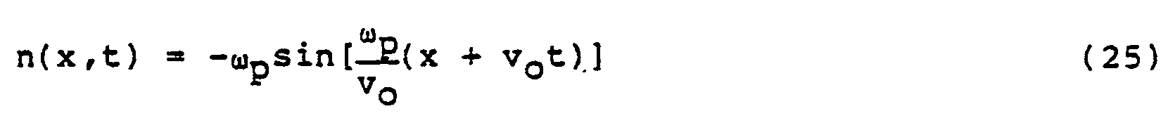
- the Green's function solution for n ⁇ (x + v o t) is considered, i.e., for a delta-function trough which is fixed in the frame of the grating.
- the solution to Equation 24 for this n a is:
- the frequency excited is ⁇ p .
- a sum over many ⁇ functions for n a gives the same frequency of excitation.
- the periodic space-charge structure above the grating has been seen to play an important role in giving high intensity radiation, other means of creating this structure can be considered besides scattering electrons from the grating.
- the periodic space-charge structure may be created by means other than scattering an electron beam from a grating, e.g., by using a periodic Pierce electrode structure to create sheets of charged particles transverse to beam as well as to create induced surface current.
- Periodic Pierce electrode structures are well known, e.g., "ICF Neutralized Light Ion Beam Studies with Ballistic Focusing, Time Compression and Low Temperature Source", D. B. Chang and W. Salisbury, 1980 IEEE International Conference on Plasma Science, May 19-21, 1980.
- a periodic Pierce electron gun may be employed which comprises an electron emitter, a low voltage, space-charge limited, extraction and acceleration gap, and a high voltage, source limited acceleration and focusing gap.
- This structure is illustrated in FIG. 5b, where the extraction and acceleration gap 110 is between the electron emitter 105 and extraction grid 115.
- the high voltage acceleration and focusing gap 120 is disposed between the extraction grid and the acceleration grid 125.
- the beam is perferably uniform in one dimension with a 1 mm periodic Pierce electron gun structure is analogous to the structure of periodic ion injectors designed for inertial confinement fusion applications.
- Another way to increase the radiation intensity is to place the beam-grating structure inside a cavity.
- An exemplary structure is shown in FIG. 6.
- An essential difference between this resulting cavity device and existing cavity devices such as the above-noted Orotron and Ledatron devices is that the periodic space-charge structure extending far above the grating would allow electrons distant from the grating to interact resonantly with the cavity field instead of just those electrons within a grating spacing of the grating. This results from the fact that, in these known devices, the electron beam does not impinge on the grating. With this technique, it is expected that higher electron densities and more clearly defined sheets of electrons with more sharply defined boundaries will be obtained. The electron sheets need not be perpendicular to the electrode structure.
- FIG. 7 An illustrative embodiment of a radiation source employing a superconducting cavity is shown in FIG. 7.
- the grating 200 and cavity 210 are disposed within evacuated helium dewar 220 to reduce the temperature of the cavity 210 to below 20K.
- the cavity 210 is fabricated from a superconductor material, such as Nb 3 Sn; alternatively, a thin film of superconductive material may be formed on the grating side of a substrate.
- the electron beam generator (not shown) need not be disposed within dewar 220, but rather may be disposed to communicate the electron beam 230 through an opening 225 so as to impinge on the grating at a glancing angle.
- the resulting radiation 250 may be emitted from the dewar through window port 240.
- the superconductive material has a near total loss of resistance at a critical temperature that is characteristic of each material.
- the cavity mirror becomes less lossy, enhancing the intensity of the emitted radiation.
- the cavity may also be constructed so that the reflecting faces capture the radiation at those angles for which maximum intensity occurs. This may require a cavity with three reflectors (including the grating), for instance, rather than two.
- An illustrative structure is shown in FIG. 8.
- a radiation source employing a planar mirror is illustrated.
- a planar mirror 300 is supported above the grating 310, with the mirror surface 305 facing the grating.
- the electron beam 320 is passed between the grating and mirror surface.
- the mirror may be placed very close to the grating so that the generated radiation 325 can be amplified in the slow wave space-charge sheets through a great number of bounces between the mirror and the grating.
- Another way to increase the intensity is to orient the blaze angle of the grating so as to enhance either a cavity mode or the radiation in the direction of maximum intensity. It may also be of advantage to make the grating depth equal to a quarter wavelength in order to force the radiation intensity to be larger in directions away from the grating.
- FIGS. 10-(a)-(c) illustrate graphically the determination of the angle at which maximum intensity occurs.
- FIG. 10(a) represents the amplitude of the radiation emitted as a result of induced surface currents as a function of the viewing angle 8 (Equation 7).
- FIG. 10(b) depicts the amplification of radiation passing through the space-charge structure, as a function of the viewing angle 8 and for a particular angular orientation of the space-charge structure in relation to the grating (Equation 25).
- FIG. 10(c) represents the produce of the emission amplitude (10(a)) and amplification factor (8(b)). The resulting product curve then has an amplitude peak at a particular observation angle 8 c .
- the amplification should be varied as a function of this angle, and the product of the amplification and emission amplitude recalculated to optimize the peak. This is illustrated by the three curves shown in FIG. 10(d), each representing the product resulting from a particular angular orientation of the space-charge sheets.
- the grating blaze angle may be selected so as to result in the space-charge sheets being directed in the angle for which the maximum intensity is obtained.
- the radiation source described above provides a means of simultaneously giving radiation at several different wavelengths, with the interesting feature that there would be a definite correlation between the phases of the radiation at different wavelengths. This can be done by using several beams of electrons of different energies, since the wavelength emitted by any electron depends on its velocity according to Equation 1. Alternatively, a wide electron beam may be employed which impacts on two or more gratings of different grating spacing widths, exploiting variation of another parameter of Equation 1. Yet another technique is to employ two or more gratings of the same grating spacing but with one or more oriented obliquely with respect to the beam direction so that the effective grating spacing is narrowed.
- the radiation from the radiation source can also be modulated, both in frequency and in amplitude.
- the former can be achieved easily by varying the acceleration voltage for the electron beam.
- the latter can be obtained by deflecting the beam transversely, so that the number of electrons impacting the grating may be varied. Transverse deflection can be achieved by applying a small voltage to the grating itself.
- the periodic space-charge structure can be obtained either by Bragg reflecting electrons from these lattices, or transmitting charged particles through the lattices to created sheets of space-charge. Channeling would help define the sheets in the latter case.
- the beam would have to be very well collimated in order that the space-charge periodicity would extend an appreciable distance from the grating.
- the surfaces of the crystal or semiconductor need to be conductive so as to set up the surface currents which create the radiation.
- the conductivity needs to be high enough to drain the charge from the grating to prevent the surface charge from repelling the electron beam. In the case of the semiconductor, its conductivity may be sufficient for this purpose.
- the electron beam would strike the grating at a grazing angle, to optimize the number of electrons which are reflected from the grating so as to set up the periodic space-charge structure. It has been found that if the electron beam strikes the grating at angles larger than grazing angles so that a significant number of electrons are trapped in the grating rather than being reflected, significant broadband noncoherent radiation is generated. Electrons which are trapped within the grating material are decelerated, and this change in velocity gives rise to Bremsstrahling radiation, a well-known phenomenon. This radiation is broadband and noncoherent. In fact, this type of radiation can be generated by impacting the electron beam onto a polished surface. This property can be exploited to provide an added capability to the radiation source of the present invention. Thus, in FIG. 1, the grating may simply be tilted to a significant angle with respect to the incident beam. Significant broadband radiation will be produced as a result.
Landscapes
- Physics & Mathematics (AREA)
- Electromagnetism (AREA)
- Engineering & Computer Science (AREA)
- Plasma & Fusion (AREA)
- Optics & Photonics (AREA)
- Particle Accelerators (AREA)
- Analysing Materials By The Use Of Radiation (AREA)
- Electron Sources, Ion Sources (AREA)
Abstract
Description
- The present invention relates to radiation sources employing an electron beam reflecting from a conductive grating.
- Radiation from electrons interacting with a diffraction grating has been studied both theoretically and experimentally since the early work of W. W. Salisbury described in U.S. Patent No. 2,634,372 and in J. Opt. Soc. Am., Vol. 60, page 1279 et seq. (1970), and the work of S. J. Smith and E. M. Purcell as described in Phys. Rev., Vol. 92, page 1069 et seq. (1953). As described in these references, an electron beam interacting with the surface of a metallic grating has been shown to generate electromagnetic radiation. This radiation source is easily tunable, with the wavelength X depending on the grating period a, electron speed vo and the angle 6 between the electron velocity and observation direction as shown in Equation 1, where c is the velocity of light.

- Past theoretical treatments of the radiation from an electron beam interacting with the surface of a metallic grating are understood to have assumed that the electrons do not collide with the grating. With this assumption, both incoherent and coherent radiation have been discussed.
- The incoherent radiation has been discussed in terms of dipole radiation from oscillating image changes (S. J. Smith and E. M. Purcell, Physics Review, Vol. 92, page 1069 (1953)), grating scattering of the evanescent waves tied to the electrons (E. Labor, Physics Review, Vol. A7, page 435 (1973); G. Toraldo di Francia, Nuovo Cimento, Vol. 16, page 61 (1960)), and rigorous Green's function formulations of the electromagnetic fields generated in the half-space grounded by the grating (C. W. Barnes and K. G. Dedrick, J. Appl. Phys., 37, 411 (1966); P. M. Van den Berg and T. H. Tan, J. Opt. Soc. Am., 64, 325 (1974)).
- The generation of coherent radiation has been discussed in connection with the situation when the electron beam and grating are placed within a resonant cavity. The resulting device has been called the oratron or ledatron. (F. S. Rusin and G. D. Bogomolov, JETP Lett., 4, 160 (1966); K. Mizuno, S. Ono, and Y. Shibata, IEEE Trans. Electron Devices, ED-20,749 (1973)). In that case, the coherent radiation produced has been treated by calculating the power transferred from an electron beam to a cavity mode which is perturbed by the periodic grating. R. P. Leavitt, D. E. Wortman, and C. A. Morrison, Appl. Phys. Lett., 35, 363 (1979); R. P. Leavitt and D. E. Wortman, J. Appl. Phys., 54, 2219 (1983).
- In none of the foregoing analyses are the electrons assumed to collide with the grating. There is, however, some experimental work indicating that electron collisions with the grating should make an appreciable difference. The early experiments of W. Salisbury with low divergence beams scattering off the grating, discussed in the paper "Generation of Light from Free Electrons", Winfield W. Salisbury, Journal of the Optical Society of America, Winfield W. Salisbury, Vol. 60, No. 10, Oct. 1970, pp. 1279-1284, disclosed the following significant differences from the Smith-Purcell-type experiments in which no electron collisions with the grating occurred.
- 1. The radiation intensity was much larger with very bright colors appearing even when overhead illumination was present;
- 2. electrons which were 1 mm from the grating contributed as much as electrons within a grating spacing of the grating; and
- 3. the radiation intensity was largest when the numbers of scattered and unscattered electrons were comparable.
- The second finding above is in direct contradiction to theoretical calculations which assume that no collisions with the grating occur. These calculations indicate that electrons which are farther away from the grating than one grating spacing should produce negligible radiation.
- Insofar as is known to applications, the above-referenced research efforts have not resulted in explanations of the underlying radiation phenomena, which has, in turn, limited the usefulness of the phenomena.
- It is, therefore, an aim of the present invention to provide a radiation source resulting from an understanding of the emission of radiation from the reflection of electrons from a grating.
- Preferably the present invention provides a radiation source which is easily tunable over a broad band of wavelengths and which can provide either coherent or noncoherent radiation.
- It is also preferable that the radiation source may be easily modulated both in frequency and in amplitude.
- According to the present invention there is provided a radiation source employing an electrically conductive grating, electron beam means for directing at least one beam of electrons above the grating so as to generate spontaneous radiation from the interaction of the electron beam and the conductive grating and means for providing a periodic space-charge structure of electrons above the grating such that the spontaneous radiation passes through said space-charge structure and thereby experiences an amplification gain, characterised in that said grating has a grating element spacing a; and said electron beam means directs a plurality of beams of electrons of different electron energies through said periodic space-charge structure, whereby spontaneous radiation of different wavelengths is generated from the interaction of the electron beams and the grating, and whereby the wavelengths of the radiation are dependent on the electron energies and the grating spacing a.
- According to another aspect of the present invention there is provided a radiation source employing an electrically conductive grating, electron beams means for directing a beam of electrons above the grating so as to generate spontaneous radiation from the interaction of the electron beam and the conductive grating and means for providing a periodic space-charge structure of electrons above the grating such that the spontaneous radiation passes through said space-charge structure and thereby experiences an amplification gain, characterised in that said electrically conductive grating has a plurality of grating elements having a first effective grating element spacing in a first region and a second effective grating element spacing in a second region of said grating; whereby spontaneous radiation of two different wavelengths is generated from the interaction of the electron beam and the two regions of the grating, and whereby the radiation wavelengths are dependent on the electron energy and the grating element spacings.
- Specific embodiments, features and advantages of the present invention are now described by way of example only with reference to the accompanying drawings, in which:-
- FIG. 1 is a general schematic diagram of a radiation source which employs the interaction of an electron beam and a grating;
- FIG. 2 is a graph which compares the angular distribution of the Smith-Purcell-type radiation density derived in accordance with the invention (solid curve) with the values obtained by known Green's function formulations (dashed curve);
- FIG. 3 illustrates a simple model of the structure for generating Salisbury-type radiation;
- FIGS. 4a-4c are graphs plotting the energy transfer from electrons to the radiation field in accordance with the invention for representative parameters.
- FIGS. 5a and 5b show simplified diagrams of an alternate embodiment of the invention, wherein the periodic space-charge structure is created by an accelerating grid structure oriented so as to inject sheets of electrons transverse to the radiating electron beam.
- FIG. 6 is a diagram of a radiation source employing a cavity in accordance with the invention.
- FIG. 7 is a simplified schematic drawing of a radiation source employing a cavity with a superconducting reflecting surface to increase the intensity of the emitted radiation.
- FIG. 8 is a diagram of a radiation source mounted in a cavity with reflecting faces adapted to capture radiation at predetermined angles.
- FIG. 9 is a simplified schematic view of a radiation source employing a planar mirror.
- FIGS. 10a-10d are graphs illustrating respectively the relationship between the observation angle and the amplitude of induced surface current radiation, the gain resulting from the space-charge structure and the product function of the amplitude and amplification functions, for a radiation source in accordance with the invention.
- FIGS. 11 a and 11b are simplified diagrams of features of a radiation source in accordance with the invention, wherein a crystalline and superlattice structure are respectively employed as the grating.
- The present invention comprises a novel radiation source. The following description is presented to enable any person skilled in the art to make and use the invention. Various modifications to the preferred embodiments will be readily apparent to those skilled in the art, and the generic principles defined herein may be applied to other embodiments and applications. Thus, the present invention is not intended to be limited to the embodiments shown, but is to be accorded the widest scope consistent with the principles and novel features disclosed herein.
- The invention comprises a radiation source employing the interaction of an electron beam with a conductive grating. FIG. 1 discloses a simplified schematic diagram of the system. The elements are enclosed in
chamber 20, which is evacuated preferably to a pressure of about 10-3 Torr or below (1 Torr = 133 Pa). Theconductive grating 10 is disposed in thechamber 20, mounted on adjustingscrews 15 which permit translating and tilting of the grating position from outside the vacuum chamber. - An
electron beam gun 30 is disposed withinchamber 20 and is adapted to generate anelectronic beam 40. In the disclosed embodiment, thegun 30 is a Pierce electron gun, comprising athermionic cathode 32 as a source of free electrons, an accelerating grid 34 andcollimating plates 36 for collimating theresultant electron beam 40. The acceleration voltage is adjustable. (In experiments conducted by applicants, acceleration voltages up to 150 kV have been used and higher accelerations would be beneficial in some applications.) - The
electron beam 40 is directed over thegrating 10. The distance between the beam and the grating, and the beam incidence angle, can be adjusted by translating and tilting the grating from outside the vacuum chamber. Anelectron catcher 50 is disposed in the chamber, opposite the grating from the electron gun so as to trap the unscattered electrons after passing the grating. Windows 60 are provided in the enclosure defining the evacuatedchamber 20 for escape of theradiation 70 generated by the electron beam. - As was discussed above, several theoretical discussions have appeared in the literature concerning the case with no electron collisions with the grating. This is the case when the
electron beam 40 as shown in FIG. 1 is not allowed to graze thegrating 10. These discussions range from the original idea of Smith and Purcell of dipole radiation from an oscillating image charge in the grating, though calculations of the scattering from the grating of the evanescent waves tied to the electrons, to rigorous Green's function formulations of the electromagnetic fields generated in the region bounded by the conduction grating. (S. J. Smith and E. M. Purcell, Phys. Rev., 92, 1069 (1953); E. Labor, Phys. Rev., A7, 435 (1973); G. Toraldo di Francia, Nuovo Cimento, 16, 61 (1960)TC. W. Barnes and K. G. Dedrick, J. Appl. Phys., 37, 411 (1966); P. M. Van Den Berg and T. H. Tan, J. Opt. Soc. Am., 64, 325 (1964)). - The angular distribution of the radiation intensity predicted by the simple oscillating image charge analog is quite different from that predicted by the rigorous Green's function calculations. The former gives a characteristic dipole radiation pattern with the major lobes in the directions defined by the electron path; as the electron energy increases, the lobe in the direction of the electron's motion increase, while the backward lobe decreases, (W. W. Salisbury, U.S. Patent No. 2,634,372 (1949); W. W. Salisbury, J. Opt. Soc. Am., 60, 1279 (1970)). On the other hand, the Green's function approach appears to give the main lobe in the backward direction. (P. M. Van den Berg, J. Opt. Soc. Am., 63, 1588 (1973)). The results of the rigorous Green's function treatments are expressed in terms of perturbation expansions, and these are sufficiently complex that the underlying physical occurrences can be obscured.
- One aspect of the invention is the provision of a simple model of the radiation mechanism which emphasizes the underlying physics and illustrates why the image charge and Green's function approaches lead to such different results.
- An approximate expression may be obtained for the surface current density


- If the undulating geometry of the diffraction grating is added as a simple sinusoidal perturbation of wave number


- For an observation point in the x-y plane defined by the electron velocity and the perpendicular to the grating at an angle e above the grating, this current density gives:


- FIG. 2 compares this simple expression with the numerical results obtained by the Green's function formulations. The angular distribution of intensity compares well. In FIG. 2, the solid curve represents the simple model of Equation 7 and the dashed curve depicts the results of the Green's function formulation.
- Following his early experiments, Salisbury proposed that the electrons reflected from the grating formed sheets of space-charge having the same periodicity as the grating. W. W. Salisbury, U.S. Patent No. 2,634,372 (1949); W. W. Salisbury, J. Opt. Soc. Am., 60, 1279 (1970). Other electrons passing through these sheets of space-charge would then be alternately accelerated and decelerated by the electrostatic forces between them and the electrons comprising the space-charge sheets. Since the space-charge would occupy the region even far from the grating, this would permit distant electrons to radiate as well as electrons that are close to the grating. Thus, in this hypothesis, in addition to the surface currents responsible for the radiation in the Smith-Purcell-type experiment (where the electrons do not scatter from the grating), bulk currents in the space above the grating can also contribute.
- To describe the characteristics of this "Salisbury" radiation, a simple model is considered in which electrons scatter off the surface at an angle e, creating potential troughs through which the unscattered electrons then move. This is illustrated in FIG. 3.
- For a grating of spatial period a, the troughs will have a period a in the x-direction and a period a/tan8 in the y-direction, where coordinate axes have chosen so that x lies parallel to the grating along the direction of the unscattered electron velocity, and the y-direction is perpendicular to this grating, and the y-direction is perpendicular to this grating. The basic features of the radiation to determine in this model can be calculated from a crude approximation by which the electrostatic potential ΦG of the troughs is given by only the lowest term in its harmonic expansion:


- Electrons moving through this potential will radiate, with the energy dεω radiated into the element of solid angle dn in the k-direction, in the form of waves with frequencies in the angular frequency interval dω. The incoherent portion dεinc of the radiation arises from the uncorrelated motion of the electrons. By similar analysis which led to Equation 7, it can be shown that:


- The spontaneous radiation due to surface currents is much greater in intensity than the spontaneous radiation arising from acceleration of the electrons in the potential troughs created by the scattered electrons. This is because the amplitude of the perturbations in the surface currents due to the grating is much larger than the perturbations in the electron trajectory due to the potential troughs. The former is of the order of b, the grating amplitude (equal to one-half the grating depth), while the latter is of the order of eδψ/mvoω where 30 is the potential due to the troughs, m is the electron mass, and ω is of the order of kgvo. From Poisson's equation, δψ~kg -2mse where ms is the density of scattered electrons. Thus, since the spontaneous radiation intensity is proportional to the square of the perturbation amplitude, the ratio of the surface current radiation to the trough radiation is of the order of magnitude given in Equation 16.

- For typical parameters in Salisbury's early experiments, b = 10-14 cm, kg = 104 cm-1, mv

- In order for an electron beam to amplify an electromagnetic wave, the electrons must interact resonantly with the wave, i.e., the wave must have a component with a phase velocity whose projection in the direction of the electron motion is equal to or less than the electron velocity. The periodic space charge created by the electrons reflecting from the grating makes possible this situation. Thus, an electromagnetic wave which in the absence of this periodic space-charge structure would have the dependence


- The phase velocity of the nth sideband is ω/|k + nk.1 and can be equal to or even less than an electron velocity. This permits resonant transfer of energy from the electrons to the waves, resulting in considerable amplification of the radiation. As an example, it is assumed that the unperturbed electron distribution is described by the distribution function:

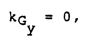
- This describes a group of electrons of temperature T and average density no drifting with velocity vo in the y-direction. Boltzmann's constant is indicated by k, and the presence of electrons scattered from the periodic grating surface is described by the ξ cos(kGxx+kGyy) term.
- Solution of Maxwell's equation with the equations of motion leads to the result that the energy transferred per second from the electrons in a unit volume to the radiation field is |A + B + C + D|, where:


- In the above it has been assumed that ω = (kx+kgx)vo + δv(kx+kGx) where δv is some fraction 0(1) of the thermal velocity. The above dispersion condition plus the radiation condition ω = kc implies that:


- FIGS. 4a, 4b, 4c show normalized plots of energy transfer from electrons to the radiation field for representative parameters and for different values of electron density, no. In the figures, the following list of parameters is used, with:
- a = 10-4 cm
- kGx = 2 f/a
- kGy = -10 kGx
- vo = 2 x 1010 cm/sec
- T = 100°k

- It is therefore apparent from the foregoing that coherent radiation can be obtained even in the absence of a cavity when electrons are reflected from a grating. The condition for the coherent radiation to dominate the incoherent radiation is that the spontaneous radiation from the induced surface currents must experience an (inverse Landau damping) amplification gain greater than unity on moving through the periodic space-charge structure above the grating. An amplification gain greater than unity occurs when the total average energy transfer from the electrons to the radiation field is greater than the energy radiated by the induced surface currents (given in Equation 7). The gain G is equal to the ratio I/Iinput, where:
- I = ∫ dv3[A + B + C + D]/r.
- Iinput is given by Equation 7 and is the radiation intensity from the induced surface currents.
- The amplification gain greater than unity occurs for reasonable parameter values when the electron beam is thick enough, dense enough, and well collimated enough to give a well defined periodic space-charge structure on reflection. By way of example only, the following are presently considered reasonable parameter values: .1 to 1 milliradian beam divergence, beam densities on the order of 108 particles/cm2, particle energies on the order of 100 kV, and grating spacings on the order of 1000 nm. These values are exemplary only; other values are also reasonable and attainable.
- If the space-charge structure is not well-defined, there would not be an effective mechanism to impart energy from the electron beam to the radiation generated by the grating surface currents.
- Coherent radiation can also arise from the correlated motion of the electrons.
Equation 20 gives the radiation vector potential as an integral over

-
Equation 20 shows that if


- To determine if electrons moving through the potential troughs can give rise to a large microscopic current variation of the form


- This occurs when these equations are solved through second order in ΦG.
- Solution of these equations give current densities which have spatial and time variations of the form:
- (a) e-i(ωst - ksxx - ksyY)
- (b) ei(kGxx + kGyY)
- (c) e-i(ωst - (ksx ± kGx)x - (ksy ± kGy)y)
- Thus, jω varies as

- ω = ωs (23a)
- kx = ksx ± kGx (23b)
- ky = ksy ± kGy (23c)
- this component will give rise to coherent radiation.
- To determine what frequencies ωs are likely to be excited in the beam of interaction with the troughs, the equation for the density of the beam in the frame x moving with the beam is considered.

- As a result, it is apparent that collective effects can be used to enhance the intensity of coherent radiation from an electron beam scattering off a diffraction grating. This will occur when the plasma frequency &)p of the beam is comparable to the radiation frequency. The latter is of the order of vJa, where vo is the electron velocity and a is the grating spacing. This is presently a practical condition for mm-wave frequencies.
- From the foregoing, additional ways may be seen to improve the performance of a radiation source based on the interaction of electrons with a conductive grating. Since the periodic space-charge structure above the grating has been seen to play an important role in giving high intensity radiation, other means of creating this structure can be considered besides scattering electrons from the grating. One way, for instance, to have an accelerating grid structure oriented so as to inject sheets of electrons transverse to the radiating electron beam. This is illustrated in FIG. 5a. Accordingly, the periodic space-charge structure may be created by means other than scattering an electron beam from a grating, e.g., by using a periodic Pierce electrode structure to create sheets of charged particles transverse to beam as well as to create induced surface current. Periodic Pierce electrode structures are well known, e.g., "ICF Neutralized Light Ion Beam Studies with Ballistic Focusing, Time Compression and Low Temperature Source", D. B. Chang and W. Salisbury, 1980 IEEE International Conference on Plasma Science, May 19-21, 1980. In this embodiment, for example, a periodic Pierce electron gun may be employed which comprises an electron emitter, a low voltage, space-charge limited, extraction and acceleration gap, and a high voltage, source limited acceleration and focusing gap. This structure is illustrated in FIG. 5b, where the extraction and
acceleration gap 110 is between theelectron emitter 105 andextraction grid 115. The high voltage acceleration and focusinggap 120 is disposed between the extraction grid and theacceleration grid 125. The beam is perferably uniform in one dimension with a 1 mm periodic Pierce electron gun structure is analogous to the structure of periodic ion injectors designed for inertial confinement fusion applications. - Another way to increase the radiation intensity is to place the beam-grating structure inside a cavity. An exemplary structure is shown in FIG. 6. An essential difference between this resulting cavity device and existing cavity devices such as the above-noted Orotron and Ledatron devices is that the periodic space-charge structure extending far above the grating would allow electrons distant from the grating to interact resonantly with the cavity field instead of just those electrons within a grating spacing of the grating. This results from the fact that, in these known devices, the electron beam does not impinge on the grating. With this technique, it is expected that higher electron densities and more clearly defined sheets of electrons with more sharply defined boundaries will be obtained. The electron sheets need not be perpendicular to the electrode structure.
- For these cavity devices several ways of increasing the intensity are apparent. An illustrative embodiment of a radiation source employing a superconducting cavity is shown in FIG. 7. The grating 200 and
cavity 210 are disposed within evacuated helium dewar 220 to reduce the temperature of thecavity 210 to below 20K. Thecavity 210 is fabricated from a superconductor material, such as Nb3Sn; alternatively, a thin film of superconductive material may be formed on the grating side of a substrate. The electron beam generator (not shown) need not be disposed within dewar 220, but rather may be disposed to communicate theelectron beam 230 through anopening 225 so as to impinge on the grating at a glancing angle. The resultingradiation 250 may be emitted from the dewar throughwindow port 240. - The superconductive material has a near total loss of resistance at a critical temperature that is characteristic of each material. Thus, as the cavity material is cooled below its critical temperature, the cavity mirror becomes less lossy, enhancing the intensity of the emitted radiation.
- With the Q of the cavity much larger than that of present devices, this will permit the resonant fields to increase so that more energy can be transferred between the beam electrons and the field.
- The cavity may also be constructed so that the reflecting faces capture the radiation at those angles for which maximum intensity occurs. This may require a cavity with three reflectors (including the grating), for instance, rather than two. An illustrative structure is shown in FIG. 8.
- Referring now to FIG. 9, a radiation source employing a planar mirror is illustrated. In this embodiment a
planar mirror 300 is supported above thegrating 310, with themirror surface 305 facing the grating. Theelectron beam 320 is passed between the grating and mirror surface. The mirror may be placed very close to the grating so that the generatedradiation 325 can be amplified in the slow wave space-charge sheets through a great number of bounces between the mirror and the grating. - Another way to increase the intensity is to orient the blaze angle of the grating so as to enhance either a cavity mode or the radiation in the direction of maximum intensity. It may also be of advantage to make the grating depth equal to a quarter wavelength in order to force the radiation intensity to be larger in directions away from the grating.
- To determine the direction of the maximum intensity, the magnitude of emitted radiation from induced surface currents must be considered as well as the radiation amplification in the space-charge sheets. The former factor is calculated by Equation 7; the latter factor results from the solution of Equation 25. FIGS. 10-(a)-(c) illustrate graphically the determination of the angle at which maximum intensity occurs. FIG. 10(a) represents the amplitude of the radiation emitted as a result of induced surface currents as a function of the viewing angle 8 (Equation 7). FIG. 10(b) depicts the amplification of radiation passing through the space-charge structure, as a function of the
viewing angle 8 and for a particular angular orientation of the space-charge structure in relation to the grating (Equation 25). FIG. 10(c) represents the produce of the emission amplitude (10(a)) and amplification factor (8(b)). The resulting product curve then has an amplitude peak at aparticular observation angle 8c. - Because the magnitude of the amplification through the space-charge sheets is dependent on their angular relationship to the grating, the amplification should be varied as a function of this angle, and the product of the amplification and emission amplitude recalculated to optimize the peak. This is illustrated by the three curves shown in FIG. 10(d), each representing the product resulting from a particular angular orientation of the space-charge sheets.
- Once the angular orientation of the space-charge sheets and the observation angle has been determined for which the maximum intensity is obtained, then the grating blaze angle may be selected so as to result in the space-charge sheets being directed in the angle for which the maximum intensity is obtained.
- The radiation source described above provides a means of simultaneously giving radiation at several different wavelengths, with the interesting feature that there would be a definite correlation between the phases of the radiation at different wavelengths. This can be done by using several beams of electrons of different energies, since the wavelength emitted by any electron depends on its velocity according to Equation 1. Alternatively, a wide electron beam may be employed which impacts on two or more gratings of different grating spacing widths, exploiting variation of another parameter of Equation 1. Yet another technique is to employ two or more gratings of the same grating spacing but with one or more oriented obliquely with respect to the beam direction so that the effective grating spacing is narrowed.
- The radiation from the radiation source can also be modulated, both in frequency and in amplitude. The former can be achieved easily by varying the acceleration voltage for the electron beam. The latter can be obtained by deflecting the beam transversely, so that the number of electrons impacting the grating may be varied. Transverse deflection can be achieved by applying a small voltage to the grating itself.
- It is of interest to consider the extension of this technique to x-ray wavelengths, e.g., to construct a compact x-ray laser. This requires a grating with a small spatial period. Crystals (e.g., Cu, Ni, Si) can be used for this purpose for spatial periods which are on the order of Angstroms. Superlattices can be used for 0(1-10 nm) periods. Exemplary structures are shown in FIGS. 11 (a) and 11 (b), respectively, employing the crystalline and superlattice structure. As is shown, the superlattice structure is a semiconductor doped with impurities (indicated by "x" in FIG. 11(b)). The periodic space-charge structure can be obtained either by Bragg reflecting electrons from these lattices, or transmitting charged particles through the lattices to created sheets of space-charge. Channeling would help define the sheets in the latter case. For the reflection mode of operation, the beam would have to be very well collimated in order that the space-charge periodicity would extend an appreciable distance from the grating. The surfaces of the crystal or semiconductor need to be conductive so as to set up the surface currents which create the radiation. The conductivity needs to be high enough to drain the charge from the grating to prevent the surface charge from repelling the electron beam. In the case of the semiconductor, its conductivity may be sufficient for this purpose.
- The above embodiments have contemplated that the electron beam would strike the grating at a grazing angle, to optimize the number of electrons which are reflected from the grating so as to set up the periodic space-charge structure. It has been found that if the electron beam strikes the grating at angles larger than grazing angles so that a significant number of electrons are trapped in the grating rather than being reflected, significant broadband noncoherent radiation is generated. Electrons which are trapped within the grating material are decelerated, and this change in velocity gives rise to Bremsstrahling radiation, a well-known phenomenon. This radiation is broadband and noncoherent. In fact, this type of radiation can be generated by impacting the electron beam onto a polished surface. This property can be exploited to provide an added capability to the radiation source of the present invention. Thus, in FIG. 1, the grating may simply be tilted to a significant angle with respect to the incident beam. Significant broadband radiation will be produced as a result.
- It is understood that the above-described embodiments are merely illustrative of the many possible specific embodiments which can represent principles of the present invention.
Claims (8)
Applications Claiming Priority (2)
| Application Number | Priority Date | Filing Date | Title |
|---|---|---|---|
| US06/777,893 US4727550A (en) | 1985-09-19 | 1985-09-19 | Radiation source |
| US777893 | 2004-02-12 |
Publications (2)
| Publication Number | Publication Date |
|---|---|
| EP0237559A1 EP0237559A1 (en) | 1987-09-23 |
| EP0237559B1 true EP0237559B1 (en) | 1991-12-27 |
Family
ID=25111626
Family Applications (1)
| Application Number | Title | Priority Date | Filing Date |
|---|---|---|---|
| EP86906048A Expired EP0237559B1 (en) | 1985-09-19 | 1986-09-08 | Radiation source |
Country Status (6)
| Country | Link |
|---|---|
| US (1) | US4727550A (en) |
| EP (1) | EP0237559B1 (en) |
| JP (1) | JPH0668560B2 (en) |
| DE (1) | DE3683147D1 (en) |
| IL (1) | IL79806A0 (en) |
| WO (1) | WO1987001873A1 (en) |
Cited By (23)
| Publication number | Priority date | Publication date | Assignee | Title |
|---|---|---|---|---|
| US7253426B2 (en) | 2005-09-30 | 2007-08-07 | Virgin Islands Microsystems, Inc. | Structures and methods for coupling energy from an electromagnetic wave |
| US7282776B2 (en) | 2006-02-09 | 2007-10-16 | Virgin Islands Microsystems, Inc. | Method and structure for coupling two microcircuits |
| US7646991B2 (en) | 2006-04-26 | 2010-01-12 | Virgin Island Microsystems, Inc. | Selectable frequency EMR emitter |
| US7655934B2 (en) | 2006-06-28 | 2010-02-02 | Virgin Island Microsystems, Inc. | Data on light bulb |
| US7656094B2 (en) | 2006-05-05 | 2010-02-02 | Virgin Islands Microsystems, Inc. | Electron accelerator for ultra-small resonant structures |
| US7659513B2 (en) | 2006-12-20 | 2010-02-09 | Virgin Islands Microsystems, Inc. | Low terahertz source and detector |
| US7679067B2 (en) | 2006-05-26 | 2010-03-16 | Virgin Island Microsystems, Inc. | Receiver array using shared electron beam |
| US7688274B2 (en) | 2006-02-28 | 2010-03-30 | Virgin Islands Microsystems, Inc. | Integrated filter in antenna-based detector |
| US7710040B2 (en) | 2006-05-05 | 2010-05-04 | Virgin Islands Microsystems, Inc. | Single layer construction for ultra small devices |
| US7714513B2 (en) | 2005-09-30 | 2010-05-11 | Virgin Islands Microsystems, Inc. | Electron beam induced resonance |
| US7718977B2 (en) | 2006-05-05 | 2010-05-18 | Virgin Island Microsystems, Inc. | Stray charged particle removal device |
| US7723698B2 (en) | 2006-05-05 | 2010-05-25 | Virgin Islands Microsystems, Inc. | Top metal layer shield for ultra-small resonant structures |
| US7728702B2 (en) | 2006-05-05 | 2010-06-01 | Virgin Islands Microsystems, Inc. | Shielding of integrated circuit package with high-permeability magnetic material |
| US7728397B2 (en) | 2006-05-05 | 2010-06-01 | Virgin Islands Microsystems, Inc. | Coupled nano-resonating energy emitting structures |
| US7732786B2 (en) | 2006-05-05 | 2010-06-08 | Virgin Islands Microsystems, Inc. | Coupling energy in a plasmon wave to an electron beam |
| US7741934B2 (en) | 2006-05-05 | 2010-06-22 | Virgin Islands Microsystems, Inc. | Coupling a signal through a window |
| US7746532B2 (en) | 2006-05-05 | 2010-06-29 | Virgin Island Microsystems, Inc. | Electro-optical switching system and method |
| US7791053B2 (en) | 2007-10-10 | 2010-09-07 | Virgin Islands Microsystems, Inc. | Depressed anode with plasmon-enabled devices such as ultra-small resonant structures |
| US7876793B2 (en) | 2006-04-26 | 2011-01-25 | Virgin Islands Microsystems, Inc. | Micro free electron laser (FEL) |
| US7986113B2 (en) | 2006-05-05 | 2011-07-26 | Virgin Islands Microsystems, Inc. | Selectable frequency light emitter |
| US7990336B2 (en) | 2007-06-19 | 2011-08-02 | Virgin Islands Microsystems, Inc. | Microwave coupled excitation of solid state resonant arrays |
| US8188431B2 (en) | 2006-05-05 | 2012-05-29 | Jonathan Gorrell | Integration of vacuum microelectronic device with integrated circuit |
| US8384042B2 (en) | 2006-01-05 | 2013-02-26 | Advanced Plasmonics, Inc. | Switching micro-resonant structures by modulating a beam of charged particles |
Families Citing this family (74)
| Publication number | Priority date | Publication date | Assignee | Title |
|---|---|---|---|---|
| BR8805263A (en) * | 1987-02-09 | 1989-08-15 | Tlv Co Ltd | OPERATING DETECTOR FOR CONDENSATION WATER SEPARATOR |
| JP2680369B2 (en) * | 1988-08-30 | 1997-11-19 | 浜松ホトニクス株式会社 | Electromagnetic wave device |
| US5044006A (en) * | 1990-04-27 | 1991-08-27 | Cyrulnik Reuven A | Microwave frequency modulation of x-ray beam for radio therapy treatment system |
| US5263043A (en) * | 1990-08-31 | 1993-11-16 | Trustees Of Dartmouth College | Free electron laser utilizing grating coupling |
| WO1992004747A1 (en) * | 1990-08-31 | 1992-03-19 | Trustees Of Dartmouth College | Semiconductor film free electron laser |
| US5268693A (en) * | 1990-08-31 | 1993-12-07 | Trustees Of Dartmouth College | Semiconductor film free electron laser |
| US6005916A (en) * | 1992-10-14 | 1999-12-21 | Techniscan, Inc. | Apparatus and method for imaging with wavefields using inverse scattering techniques |
| US5588032A (en) * | 1992-10-14 | 1996-12-24 | Johnson; Steven A. | Apparatus and method for imaging with wavefields using inverse scattering techniques |
| US5943422A (en) | 1996-08-12 | 1999-08-24 | Intertrust Technologies Corp. | Steganographic techniques for securely delivering electronic digital rights management control information over insecure communication channels |
| EP1643340B1 (en) * | 1995-02-13 | 2013-08-14 | Intertrust Technologies Corp. | Secure transaction management |
| US5892900A (en) * | 1996-08-30 | 1999-04-06 | Intertrust Technologies Corp. | Systems and methods for secure transaction management and electronic rights protection |
| US6157721A (en) * | 1996-08-12 | 2000-12-05 | Intertrust Technologies Corp. | Systems and methods using cryptography to protect secure computing environments |
| US6658568B1 (en) * | 1995-02-13 | 2003-12-02 | Intertrust Technologies Corporation | Trusted infrastructure support system, methods and techniques for secure electronic commerce transaction and rights management |
| US7841982B2 (en) * | 1995-06-22 | 2010-11-30 | Techniscan, Inc. | Apparatus and method for imaging objects with wavefields |
| US5889797A (en) * | 1996-08-26 | 1999-03-30 | The Regents Of The University Of California | Measuring short electron bunch lengths using coherent smith-purcell radiation |
| WO1998012667A2 (en) * | 1996-08-29 | 1998-03-26 | Johnson Steven A | Wavefield imaging using inverse scattering techniques |
| US5790585A (en) * | 1996-11-12 | 1998-08-04 | The Trustees Of Dartmouth College | Grating coupling free electron laser apparatus and method |
| JP2981543B2 (en) * | 1997-10-27 | 1999-11-22 | 金沢大学長 | Electron tube type one-way optical amplifier |
| US7092914B1 (en) * | 1997-11-06 | 2006-08-15 | Intertrust Technologies Corporation | Methods for matching, selecting, narrowcasting, and/or classifying based on rights management and/or other information |
| JP2972879B1 (en) * | 1998-08-18 | 1999-11-08 | 金沢大学長 | One-way optical amplifier |
| JP3057229B1 (en) * | 1999-05-20 | 2000-06-26 | 金沢大学長 | Electromagnetic wave amplifier and electromagnetic wave generator |
| US6909104B1 (en) | 1999-05-25 | 2005-06-21 | Nawotec Gmbh | Miniaturized terahertz radiation source |
| DE10006361A1 (en) * | 1999-05-25 | 2000-11-30 | Deutsche Telekom Ag | Miniaturized terahertz radiation source, has element such as field emitter, electrostatic lens, beam deflector, metal grid and second anode mounted on semiconducting chip by nanolithography |
| IL155030A0 (en) * | 2000-09-22 | 2003-10-31 | Vermont Photonics | Apparatuses and methods for generating coherent electromagnetic laser radiation |
| WO2002077607A2 (en) * | 2001-03-23 | 2002-10-03 | Vermont Photonics | Applying far infrared radiation to biological matter |
| US8228959B2 (en) * | 2002-09-27 | 2012-07-24 | The Trustees Of Dartmouth College | Free electron laser, and associated components and methods |
| US7771360B2 (en) * | 2003-04-09 | 2010-08-10 | Techniscan, Inc. | Breast scanning system |
| US20060009693A1 (en) * | 2004-04-08 | 2006-01-12 | Techniscan, Inc. | Apparatus for imaging and treating a breast |
| US20060062258A1 (en) * | 2004-07-02 | 2006-03-23 | Vanderbilt University | Smith-Purcell free electron laser and method of operating same |
| JP4206977B2 (en) * | 2004-07-05 | 2009-01-14 | 山田廣成 | Radiation generator |
| US20070034518A1 (en) * | 2005-08-15 | 2007-02-15 | Virgin Islands Microsystems, Inc. | Method of patterning ultra-small structures |
| US20060035173A1 (en) * | 2004-08-13 | 2006-02-16 | Mark Davidson | Patterning thin metal films by dry reactive ion etching |
| WO2007064358A2 (en) * | 2005-09-30 | 2007-06-07 | Virgin Islands Microsystems, Inc. | Structures and methods for coupling energy from an electromagnetic wave |
| US7579609B2 (en) * | 2005-12-14 | 2009-08-25 | Virgin Islands Microsystems, Inc. | Coupling light of light emitting resonator to waveguide |
| US7470920B2 (en) * | 2006-01-05 | 2008-12-30 | Virgin Islands Microsystems, Inc. | Resonant structure-based display |
| US20070152781A1 (en) * | 2006-01-05 | 2007-07-05 | Virgin Islands Microsystems, Inc. | Switching micro-resonant structures by modulating a beam of charged particles |
| US7619373B2 (en) * | 2006-01-05 | 2009-11-17 | Virgin Islands Microsystems, Inc. | Selectable frequency light emitter |
| US20070190794A1 (en) * | 2006-02-10 | 2007-08-16 | Virgin Islands Microsystems, Inc. | Conductive polymers for the electroplating |
| US20070200063A1 (en) * | 2006-02-28 | 2007-08-30 | Virgin Islands Microsystems, Inc. | Wafer-level testing of light-emitting resonant structures |
| US7605835B2 (en) * | 2006-02-28 | 2009-10-20 | Virgin Islands Microsystems, Inc. | Electro-photographic devices incorporating ultra-small resonant structures |
| US20070200646A1 (en) * | 2006-02-28 | 2007-08-30 | Virgin Island Microsystems, Inc. | Method for coupling out of a magnetic device |
| US20070200071A1 (en) * | 2006-02-28 | 2007-08-30 | Virgin Islands Microsystems, Inc. | Coupling output from a micro resonator to a plasmon transmission line |
| US7558490B2 (en) * | 2006-04-10 | 2009-07-07 | Virgin Islands Microsystems, Inc. | Resonant detector for optical signals |
| US20070252089A1 (en) * | 2006-04-26 | 2007-11-01 | Virgin Islands Microsystems, Inc. | Charged particle acceleration apparatus and method |
| US20070264023A1 (en) * | 2006-04-26 | 2007-11-15 | Virgin Islands Microsystems, Inc. | Free space interchip communications |
| US7492868B2 (en) * | 2006-04-26 | 2009-02-17 | Virgin Islands Microsystems, Inc. | Source of x-rays |
| US7359589B2 (en) * | 2006-05-05 | 2008-04-15 | Virgin Islands Microsystems, Inc. | Coupling electromagnetic wave through microcircuit |
| US7442940B2 (en) * | 2006-05-05 | 2008-10-28 | Virgin Island Microsystems, Inc. | Focal plane array incorporating ultra-small resonant structures |
| US7557647B2 (en) * | 2006-05-05 | 2009-07-07 | Virgin Islands Microsystems, Inc. | Heterodyne receiver using resonant structures |
| US20070258720A1 (en) * | 2006-05-05 | 2007-11-08 | Virgin Islands Microsystems, Inc. | Inter-chip optical communication |
| US7476907B2 (en) * | 2006-05-05 | 2009-01-13 | Virgin Island Microsystems, Inc. | Plated multi-faceted reflector |
| US7569836B2 (en) * | 2006-05-05 | 2009-08-04 | Virgin Islands Microsystems, Inc. | Transmission of data between microchips using a particle beam |
| US7436177B2 (en) * | 2006-05-05 | 2008-10-14 | Virgin Islands Microsystems, Inc. | SEM test apparatus |
| US7554083B2 (en) | 2006-05-05 | 2009-06-30 | Virgin Islands Microsystems, Inc. | Integration of electromagnetic detector on integrated chip |
| US20070258675A1 (en) * | 2006-05-05 | 2007-11-08 | Virgin Islands Microsystems, Inc. | Multiplexed optical communication between chips on a multi-chip module |
| US20070272931A1 (en) * | 2006-05-05 | 2007-11-29 | Virgin Islands Microsystems, Inc. | Methods, devices and systems producing illumination and effects |
| US7342441B2 (en) * | 2006-05-05 | 2008-03-11 | Virgin Islands Microsystems, Inc. | Heterodyne receiver array using resonant structures |
| US7583370B2 (en) * | 2006-05-05 | 2009-09-01 | Virgin Islands Microsystems, Inc. | Resonant structures and methods for encoding signals into surface plasmons |
| US20070257273A1 (en) * | 2006-05-05 | 2007-11-08 | Virgin Island Microsystems, Inc. | Novel optical cover for optical chip |
| US7443577B2 (en) * | 2006-05-05 | 2008-10-28 | Virgin Islands Microsystems, Inc. | Reflecting filtering cover |
| US7586167B2 (en) * | 2006-05-05 | 2009-09-08 | Virgin Islands Microsystems, Inc. | Detecting plasmons using a metallurgical junction |
| US20070258492A1 (en) * | 2006-05-05 | 2007-11-08 | Virgin Islands Microsystems, Inc. | Light-emitting resonant structure driving raman laser |
| US7573045B2 (en) * | 2006-05-15 | 2009-08-11 | Virgin Islands Microsystems, Inc. | Plasmon wave propagation devices and methods |
| US20070274365A1 (en) * | 2006-05-26 | 2007-11-29 | Virgin Islands Microsystems, Inc. | Periodically complex resonant structures |
| US7450794B2 (en) | 2006-09-19 | 2008-11-11 | Virgin Islands Microsystems, Inc. | Microcircuit using electromagnetic wave routing |
| US7560716B2 (en) * | 2006-09-22 | 2009-07-14 | Virgin Islands Microsystems, Inc. | Free electron oscillator |
| US7808636B2 (en) * | 2007-01-11 | 2010-10-05 | Rensselaer Polytechnic Institute | Systems, methods, and devices for handling terahertz radiation |
| US8366617B2 (en) * | 2007-05-15 | 2013-02-05 | CVUS Clinical Trials, LLC | Breast scanning system |
| JP5061063B2 (en) * | 2008-05-20 | 2012-10-31 | ギガフォトン株式会社 | Extreme ultraviolet light mirror and extreme ultraviolet light source device |
| JP5061069B2 (en) * | 2008-05-20 | 2012-10-31 | ギガフォトン株式会社 | Semiconductor exposure equipment using extreme ultraviolet light |
| KR101919417B1 (en) | 2012-02-07 | 2018-11-19 | 삼성전자주식회사 | Electromagnetic wave oscillator having multi-tunnel and Electromagnetic wave generating apparatus including the electromagnetic wave oscillator |
| RU2653567C1 (en) * | 2017-03-10 | 2018-05-11 | Федеральное государственное бюджетное учреждение "Национальный исследовательский центр "Курчатовский институт" | Method of creation of laser radiation and laser implementing this method |
| CN109916862B (en) * | 2019-02-27 | 2020-06-02 | 北京大学 | Enhanced multicolor coherent SPR device and control method thereof |
| US12015236B2 (en) * | 2021-07-22 | 2024-06-18 | National Tsing Hua University | Dielectric-grating-waveguide free-electron laser |
Family Cites Families (5)
| Publication number | Priority date | Publication date | Assignee | Title |
|---|---|---|---|---|
| US2634372A (en) * | 1953-04-07 | Super high-frequency electromag | ||
| JPS495289A (en) * | 1972-04-28 | 1974-01-17 | ||
| US4571726A (en) * | 1984-03-30 | 1986-02-18 | The United States Of America As Represented By The Secretary Of The Army | High performance orotron utilizing a dense electron beam |
| US4590596A (en) * | 1984-06-15 | 1986-05-20 | The United States Of America As Represented By The Secretary Of The Army | Method and apparatus for modulating a diffraction radiation generator |
| US4545056A (en) * | 1984-06-19 | 1985-10-01 | The United States Of America As Represented By The Secretary Of The Army | Depressed collector/ribbon electron beam analyzer for a diffraction radiation generator |
-
1985
- 1985-09-19 US US06/777,893 patent/US4727550A/en not_active Expired - Lifetime
-
1986
- 1986-08-22 IL IL79806A patent/IL79806A0/en not_active IP Right Cessation
- 1986-09-08 EP EP86906048A patent/EP0237559B1/en not_active Expired
- 1986-09-08 WO PCT/US1986/001821 patent/WO1987001873A1/en active IP Right Grant
- 1986-09-08 JP JP61505078A patent/JPH0668560B2/en not_active Expired - Lifetime
- 1986-09-08 DE DE8686906048T patent/DE3683147D1/en not_active Expired - Fee Related
Cited By (26)
| Publication number | Priority date | Publication date | Assignee | Title |
|---|---|---|---|---|
| US7758739B2 (en) | 2004-08-13 | 2010-07-20 | Virgin Islands Microsystems, Inc. | Methods of producing structures for electron beam induced resonance using plating and/or etching |
| US7791290B2 (en) | 2005-09-30 | 2010-09-07 | Virgin Islands Microsystems, Inc. | Ultra-small resonating charged particle beam modulator |
| US7791291B2 (en) | 2005-09-30 | 2010-09-07 | Virgin Islands Microsystems, Inc. | Diamond field emission tip and a method of formation |
| US7253426B2 (en) | 2005-09-30 | 2007-08-07 | Virgin Islands Microsystems, Inc. | Structures and methods for coupling energy from an electromagnetic wave |
| US7714513B2 (en) | 2005-09-30 | 2010-05-11 | Virgin Islands Microsystems, Inc. | Electron beam induced resonance |
| US8384042B2 (en) | 2006-01-05 | 2013-02-26 | Advanced Plasmonics, Inc. | Switching micro-resonant structures by modulating a beam of charged particles |
| US7282776B2 (en) | 2006-02-09 | 2007-10-16 | Virgin Islands Microsystems, Inc. | Method and structure for coupling two microcircuits |
| US7688274B2 (en) | 2006-02-28 | 2010-03-30 | Virgin Islands Microsystems, Inc. | Integrated filter in antenna-based detector |
| US7876793B2 (en) | 2006-04-26 | 2011-01-25 | Virgin Islands Microsystems, Inc. | Micro free electron laser (FEL) |
| US7646991B2 (en) | 2006-04-26 | 2010-01-12 | Virgin Island Microsystems, Inc. | Selectable frequency EMR emitter |
| US7718977B2 (en) | 2006-05-05 | 2010-05-18 | Virgin Island Microsystems, Inc. | Stray charged particle removal device |
| US7723698B2 (en) | 2006-05-05 | 2010-05-25 | Virgin Islands Microsystems, Inc. | Top metal layer shield for ultra-small resonant structures |
| US7728702B2 (en) | 2006-05-05 | 2010-06-01 | Virgin Islands Microsystems, Inc. | Shielding of integrated circuit package with high-permeability magnetic material |
| US7728397B2 (en) | 2006-05-05 | 2010-06-01 | Virgin Islands Microsystems, Inc. | Coupled nano-resonating energy emitting structures |
| US7732786B2 (en) | 2006-05-05 | 2010-06-08 | Virgin Islands Microsystems, Inc. | Coupling energy in a plasmon wave to an electron beam |
| US7741934B2 (en) | 2006-05-05 | 2010-06-22 | Virgin Islands Microsystems, Inc. | Coupling a signal through a window |
| US7746532B2 (en) | 2006-05-05 | 2010-06-29 | Virgin Island Microsystems, Inc. | Electro-optical switching system and method |
| US7710040B2 (en) | 2006-05-05 | 2010-05-04 | Virgin Islands Microsystems, Inc. | Single layer construction for ultra small devices |
| US7986113B2 (en) | 2006-05-05 | 2011-07-26 | Virgin Islands Microsystems, Inc. | Selectable frequency light emitter |
| US8188431B2 (en) | 2006-05-05 | 2012-05-29 | Jonathan Gorrell | Integration of vacuum microelectronic device with integrated circuit |
| US7656094B2 (en) | 2006-05-05 | 2010-02-02 | Virgin Islands Microsystems, Inc. | Electron accelerator for ultra-small resonant structures |
| US7679067B2 (en) | 2006-05-26 | 2010-03-16 | Virgin Island Microsystems, Inc. | Receiver array using shared electron beam |
| US7655934B2 (en) | 2006-06-28 | 2010-02-02 | Virgin Island Microsystems, Inc. | Data on light bulb |
| US7659513B2 (en) | 2006-12-20 | 2010-02-09 | Virgin Islands Microsystems, Inc. | Low terahertz source and detector |
| US7990336B2 (en) | 2007-06-19 | 2011-08-02 | Virgin Islands Microsystems, Inc. | Microwave coupled excitation of solid state resonant arrays |
| US7791053B2 (en) | 2007-10-10 | 2010-09-07 | Virgin Islands Microsystems, Inc. | Depressed anode with plasmon-enabled devices such as ultra-small resonant structures |
Also Published As
| Publication number | Publication date |
|---|---|
| JPS62502145A (en) | 1987-08-20 |
| US4727550A (en) | 1988-02-23 |
| EP0237559A1 (en) | 1987-09-23 |
| JPH0668560B2 (en) | 1994-08-31 |
| DE3683147D1 (en) | 1992-02-06 |
| IL79806A0 (en) | 1986-11-30 |
| WO1987001873A1 (en) | 1987-03-26 |
Similar Documents
| Publication | Publication Date | Title |
|---|---|---|
| EP0237559B1 (en) | Radiation source | |
| Morawitz | Self-coupling of a two-level system by a mirror | |
| Leemans et al. | Observation of terahertz emission from a laser-plasma accelerated electron bunch crossing a plasma-vacuum boundary | |
| Tomchuk et al. | Optical absorption by small metallic particles | |
| Bernhardt et al. | Artificial airglow excited by high-power radio waves | |
| Petelin | On the theory of ultrarelativistic cyclotron self-resonance masers | |
| US20210345477A1 (en) | Semiconductor laser accelerator and laser acceleration unit thereof | |
| Datz et al. | Resonant coherent excitation of N6+ and Mg11+ in planar channeling: anisotropies in ionization probabilities and X-ray emission | |
| EP0802705A2 (en) | Method and apparatus for generating high energy coherent electron beam and gamma-ray laser | |
| Wang et al. | Design of a two‐dimensional square mesh metal grating coupler for a miniband transport GaAs quantum‐well infrared photodetector | |
| Darbinian et al. | Unruh radiation in linear colliders and in collisions of TeV electrons with intense laser beams | |
| Chang et al. | Compact short-wavelength free-electron laser | |
| Nikitin et al. | Synchrotron radiation from ends of straight-linear interval | |
| Eckstein | Charge fractions of reflected particles | |
| Lozovik et al. | Stimulated light backscattering from exciton bose condensate | |
| JPH03156982A (en) | Structures with increased conductivity | |
| Baryshevsky et al. | Visible surface quasi-Cherenkov FEL | |
| Lin | Effects of a dense background plasma on the dispersion of backward wave oscillators | |
| Kostyukov et al. | Ultrahigh-intensity inverse bremsstrahlung | |
| Bae et al. | Energy modulation of nonrelativistic electrons with a CO 2 laser using a metal microslit | |
| Tsintsadze et al. | Generation of low-frequency electromagnetic waves by spectrally broad intense laser pulses in a plasma | |
| Csonka | Insertion devices, future developments, limitations | |
| Kozlov | Tunable far infrared semiconductor lasers | |
| Kalmykova | Mechanism of induced transition radiation in fields of regular waves | |
| Karapetyan et al. | Amplification of electromagnetic waves in a magnetically active plasma with a nonisotropic electron velocity distribution |
Legal Events
| Date | Code | Title | Description |
|---|---|---|---|
| PUAI | Public reference made under article 153(3) epc to a published international application that has entered the european phase |
Free format text: ORIGINAL CODE: 0009012 |
|
| 17P | Request for examination filed |
Effective date: 19870409 |
|
| AK | Designated contracting states |
Kind code of ref document: A1 Designated state(s): DE FR GB IT NL SE |
|
| 17Q | First examination report despatched |
Effective date: 19890927 |
|
| GRAA | (expected) grant |
Free format text: ORIGINAL CODE: 0009210 |
|
| AK | Designated contracting states |
Kind code of ref document: B1 Designated state(s): DE FR GB IT NL SE |
|
| ET | Fr: translation filed | ||
| REF | Corresponds to: |
Ref document number: 3683147 Country of ref document: DE Date of ref document: 19920206 |
|
| ITF | It: translation for a ep patent filed | ||
| PLBE | No opposition filed within time limit |
Free format text: ORIGINAL CODE: 0009261 |
|
| STAA | Information on the status of an ep patent application or granted ep patent |
Free format text: STATUS: NO OPPOSITION FILED WITHIN TIME LIMIT |
|
| 26N | No opposition filed | ||
| PGFP | Annual fee paid to national office [announced via postgrant information from national office to epo] |
Ref country code: FR Payment date: 19940808 Year of fee payment: 9 |
|
| PGFP | Annual fee paid to national office [announced via postgrant information from national office to epo] |
Ref country code: SE Payment date: 19940815 Year of fee payment: 9 Ref country code: GB Payment date: 19940815 Year of fee payment: 9 |
|
| PGFP | Annual fee paid to national office [announced via postgrant information from national office to epo] |
Ref country code: DE Payment date: 19940824 Year of fee payment: 9 |
|
| PGFP | Annual fee paid to national office [announced via postgrant information from national office to epo] |
Ref country code: NL Payment date: 19940930 Year of fee payment: 9 |
|
| EAL | Se: european patent in force in sweden |
Ref document number: 86906048.3 |
|
| PG25 | Lapsed in a contracting state [announced via postgrant information from national office to epo] |
Ref country code: GB Effective date: 19950908 |
|
| PG25 | Lapsed in a contracting state [announced via postgrant information from national office to epo] |
Ref country code: SE Effective date: 19950909 |
|
| PG25 | Lapsed in a contracting state [announced via postgrant information from national office to epo] |
Ref country code: NL Effective date: 19960401 |
|
| GBPC | Gb: european patent ceased through non-payment of renewal fee |
Effective date: 19950908 |
|
| PG25 | Lapsed in a contracting state [announced via postgrant information from national office to epo] |
Ref country code: FR Effective date: 19960531 |
|
| PG25 | Lapsed in a contracting state [announced via postgrant information from national office to epo] |
Ref country code: DE Effective date: 19960601 |
|
| NLV4 | Nl: lapsed or anulled due to non-payment of the annual fee |
Effective date: 19960401 |
|
| EUG | Se: european patent has lapsed |
Ref document number: 86906048.3 |
|
| REG | Reference to a national code |
Ref country code: FR Ref legal event code: ST |
|
| PG25 | Lapsed in a contracting state [announced via postgrant information from national office to epo] |
Ref country code: IT Free format text: LAPSE BECAUSE OF NON-PAYMENT OF DUE FEES;WARNING: LAPSES OF ITALIAN PATENTS WITH EFFECTIVE DATE BEFORE 2007 MAY HAVE OCCURRED AT ANY TIME BEFORE 2007. THE CORRECT EFFECTIVE DATE MAY BE DIFFERENT FROM THE ONE RECORDED. Effective date: 20050908 |