EP0237374B1 - Mémoire à bulles magnétique en technologie hybride - Google Patents
Mémoire à bulles magnétique en technologie hybride Download PDFInfo
- Publication number
- EP0237374B1 EP0237374B1 EP87400240A EP87400240A EP0237374B1 EP 0237374 B1 EP0237374 B1 EP 0237374B1 EP 87400240 A EP87400240 A EP 87400240A EP 87400240 A EP87400240 A EP 87400240A EP 0237374 B1 EP0237374 B1 EP 0237374B1
- Authority
- EP
- European Patent Office
- Prior art keywords
- implanted
- magnetic bubble
- zone
- magnetic
- propagation
- Prior art date
- Legal status (The legal status is an assumption and is not a legal conclusion. Google has not performed a legal analysis and makes no representation as to the accuracy of the status listed.)
- Expired - Lifetime
Links
Images
Classifications
-
- G—PHYSICS
- G11—INFORMATION STORAGE
- G11C—STATIC STORES
- G11C19/00—Digital stores in which the information is moved stepwise, e.g. shift registers
- G11C19/02—Digital stores in which the information is moved stepwise, e.g. shift registers using magnetic elements
- G11C19/08—Digital stores in which the information is moved stepwise, e.g. shift registers using magnetic elements using thin films in plane structure
- G11C19/0875—Organisation of a plurality of magnetic shift registers
- G11C19/0883—Means for switching magnetic domains from one path into another path, i.e. transfer switches, swap gates or decoders
- G11C19/0891—Means for switching magnetic domains from one path into another path, i.e. transfer switches, swap gates or decoders using hybrid structure, e.g. ion doped layers
Definitions
- the present invention relates to a magnetic bubble memory in hybrid technology, and more particularly relates to the junction allowing a magnetic bubble to propagate from an area with non-implanted patterns to an area with deposited patterns.
- IP implanted-permalloy junction
- the magnetic bubbles are contained in a monocrystalline magnetic layer, such as a magnetic garnet film, supported by an amagnetic monocrystalline garnet. These bubbles are in the form of isolated magnetic domains, generally cylindrical, having a magnetization opposite to that of the rest of the monocrystalline magnetic layer. These magnetic bubbles are stable by application of a continuous magnetic field Hp o i perpendicular to the plane of the magnetic layer. In practice, this magnetic field is created by a permanent magnet thus ensuring the non-volatility of the information contained in the bubble memory.
- the bubbles are displaced by applying a continuous rotating field Hr in a direction parallel to the surface of the magnetic layer.
- the bubbles are moved around so-called propagation patterns.
- These patterns in the form of discs, diamonds, triangles, T etc ... can be made of a material based on iron and nickel, deposited on an insulating layer covering the magnetic layer, or else obtained by implanting ions in the upper part of the magnetic layer, through a mask to define the shape of these patterns. In the latter case, since the ion implantation is carried out only around the patterns, these patterns are called non-implanted patterns.
- the reasons for propagation are generally contiguous; due to their shape, two adjacent patterns delimit between them two cavities or hollows.
- the displacement of the bubbles along these patterns is generally done for a duration equal to one third of the period of rotation of the plane magnetic field H T , the bubbles remaining stationary in the cavities defined between two adjacent patterns, during the rest of the cycle. These cavities constitute so-called stable positions. Shift registers are thus produced in which the binary information "1" is represented by the presence of a bubble and the binary information "0" by the absence of a bubble.
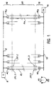
- FIG. 1 The known structure of a magnetic bubble memory is shown diagrammatically in FIG. 1. It comprises a set of loops, called minor loops, used for storing information, mutually parallel and arranged along an axis of easy magnetization 112 of the magnetic material. Each minor loop is connected by an exchange gate 4 1 , ..., 4n to a major writing loop 6 comprising at one end a magnetic bubble generator 8. The major writing loop 6 is aligned along an axis perpendicular to the axis of the minor loops; each exchange gate allows the recording of information in a minor loop.
- Each minor loop is also connected by a duplication gate 10 1 , ..., 10 n to a major read loop 12, parallel to the major write loop 6.
- the major read loop 12 ends with a detector 14 constituting a means of reading.
- a magnetic bubble memory in hybrid technology comprises two regions 16, 18 comprising deposited patterns, and a region 20 comprising non-implanted patterns. All the elements of the bubble memory are contained only in regions 16 and 18, with the exception of the minor loops which each extend over the three regions. Each minor loop therefore has four junctions, JPI-E, JIP-E, JIP-D and JPI-D, which constitute junctions between propagation paths located in different regions.
- the invention relates to junctions allowing a magnetic bubble to pass from a propagation path defined by non-implanted patterns towards a propagation path defined by deposited patterns, that is to say the junctions denoted JIP-E. and JIP-D in Figure 1.
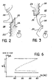
- FIGS. 2 and 3 show respectively IP-E and IP-D junctions according to the teaching of this document.
- a first propagation path is defined by a border 22 between an implanted zone 24 and a non-implanted zone 26, and a second propagation path is defined by a series of deposited patterns such as the deposited patterns 28, 30
- the two propagation paths have parallel general directions and overlap at the level of the first deposited pattern 28.
- the author proposes an improvement in the junction which consists in replacing the frank border between the implanted zone 24 and the non-implanted zone 26, where the density of implanted ions suddenly changes from a non-zero value in the implanted zone to a zero value in the non-implanted zone, by a softer border having a non-zero width or the density of implanted ions decreases linearly from a non-zero value in the implanted zone to a value zero in the non-implanted zone.
- the object of the invention is to produce a reliable IP junction, that is to say one having a large and reproducible H pol field margin without recourse to a soft border.
- a magnetic bubble passes from a propagation path defined by non-implanted patterns towards a propagation path defined by deposited patterns.
- the border between the implanted zone and the non-implanted zone is oriented perpendicular to an axis of easy magnetization of the magnetic material. Furthermore, in order to be less sensitive to the alignment between the technological levels defining the two propagation paths, the overlap area between the implanted area and the deposited pattern has an area substantially equal to that of the magnetic bubble.
- the pattern deposited it is known, to have a strong position on the pattern deposited at the level of the overlap zone, to use a pattern having the general shape of a chevron and of which one leg has a length and a particularly large width.
- this implanted zone has two functions: a first function is to limit the width of the non-implanted zone in the vicinity of the overlap zone, which weakens the stability of the magnetic bubble. On the first propagation path at this zone recovery; a second function is to push the magnetic bubble towards the end of the other leg of the rafter, while without this implanted zone the magnetic bubble tends, after having extended between the overlap zone and the end of the other leg of the rafter, to return to the overlap area if certain technological parameters vary.
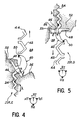
- a first propagation path is defined by the border 34 between an implanted area 36 and a non-implanted area 38
- a second propagation path is defined by a series of deposited patterns such as the patterns 40, 42 and 44.
- These two propagation paths have an identical general direction, parallel to an axis of easy magnetization 112 of the magnetic material of the memory.
- the overlap zone 46 between the paths has a surface substantially equal to the size of a magnetic bubble. This is particularly advantageous because, even in the event of poor alignment between the technological levels, it has been found experimentally that the surface of the overlap zone remains between 0.5 and 1.5 times the nominal size, and that these surface deviations do not appreciably affect the margin of the field Hp o i for crossing the magnetic bubble.
- the junction is defined so that the position of the magnetic bubble on the first propagation path in the overlap zone is a weak position for the phase of the rotating field corresponding to the crossing of the magnetic bubble, and so that the position of the magnetic bubble on the second propagation path in the overlap zone is a strong position for this phase of the rotating field.
- Obtaining a non-stable position in the implanted zone, at the level of the overlap, is obtained, according to the invention, by orienting the border 34 crossed by the magnetic bubble in a direction perpendicular to an axis of easy magnetization of the magnetic material of Memory.
- this border has a direction perpendicular to the axis 121.
- the length I of this border must be large enough to prevent the magnetic bubble from continuing to propagate along the border between the implanted area and the non-implanted area. This is obtained by choosing a length I at least equal to the step ⁇ between the non-implanted patterns defining the first propagation path.
- the strengthening of the stability of the position of the bubble on the second propagation path, at the level of the overlap zone is the result of known characteristics and of new characteristics.
- the so-called modified chevron shape of the deposited pattern 40 constituting the first deposited pattern of the second propagation path shown in FIG. 4 is known.
- the top of this chevron coincides with the overlap zone 46.
- This chevron has a large volume and has two asymmetrical legs, the leg 48 situated before the overlap zone 46 relative to the direction of propagation of the magnetic bubbles having an elongated shape to reinforce the stability of the position of a bubble located at the top of the rafter in the overlap zone.
- This known shape of the first deposited pattern 40 is not always sufficient to allow the propagation of the magnetic bubble on the second propagation path. Indeed, it has been observed that in certain cases the magnetic bubble after having stretched between the overlap zone 46 and the end 50 of the other leg of the rafter, under the influence of the rotating field H T , returns towards the overlap zone 46 instead of contracting towards the end 50 of the other leg of the rafter, if technological parameters vary.
- This drawback is eliminated in the junction of the invention by the production of an implanted area 52 extending under at least part of the wing 48 of the deposited pattern 40.
- This implanted area allows, when the bubble is stretched between the overlap zone 46 and the end 50 of the other wing of the deposited pattern 40, to create a repulsion pole towards the overlap zone 46 so that the bubble propagates by contracting towards the end 50 rather than towards the overlap zone 46.
- this implanted zone 52 extends sufficiently under the wing 48 so that the width a of the non-implanted zone in the vicinity of the overlap zone 46 is small, for example less than the pitch ⁇ between the non-implanted patterns. This thinning in fact contributes to reducing the stability of the position of the bubble on the first propagation path in the overlap zone 46.
- IP-E junction In a magnetic bubble memory in hybrid technology, two types of IP junctions are made on the minor loop. An IP-E junction is located in the vicinity of the exchange gate associated with the minor loop, and an IP-D junction is located in the vicinity of the duplication gate associated with this minor loop. The junction shown in FIG. 4 which has just been described is an IP-E junction.
- the first propagation path represented in FIG. 5 is defined by the border 34 between an implanted zone 36 and an unimplanted zone 38, and the second propagation path is defined by a series of deposited patterns such as the patterns 40, 42 and 44.
- the first deposited pattern 40 has a so-called modified chevron shape and the following patterns have a chevron shape.
- the two propagation paths have an identical general direction, parallel to an axis of easy magnetization 112 of the magnetic material of the memory.
- This axis has an identical direction but a direction opposite to the axis of propagation of the magnetic bubbles of FIG. 4.
- the overlap zone 46 has the same characteristics. dimensions (shape, size) as the overlap area shown in Figure 4.
- the border 34 between the implanted zone 36 and the non-implanted zone 38 which is crossed by the magnetic bubble has a length 1 which must be at least equal to the pitch ⁇ between the patterns non-implanted defining the first propagation path.
- This border is likewise perpendicular to the axis 112 of easy magnetization of the magnetic material of the memory.
- this border crossed by the magnetic bubble has a direction perpendicular to the general direction of propagation of the magnetic bubble, which was not the case in FIG. 4.
- this border has a direction perpendicular to the general direction of propagation of the magnetic bubble, which was not the case in FIG. 4.
- the magnetic bubble arrives in the overlap area, it tends to extend over the entire length I of the border, which can be harmful.
- the weakening of the position of the bubble on the first propagation path in the overlap zone and the strengthening of the position of this bubble on the second propagation path in the overlap zone are obtained in the same way as in the junction IP-E shown in FIG. 4.
- the first deposited pattern 40 is thus preferably a large volume pattern in the form of a chevron comprising a wing 48 creating a strong pole at the level of the overlap zone 46.
- an implanted area 52 is produced under at least a significant part of this wing 48 to further strengthen the position of the bubble on the second propagation path, in the overlap area.
- this implanted zone 52 also contributes to weakening the position of the bubble on the first propagation path.
- the implanted zone 52 makes it possible to push the magnetic bubble towards the end 50 of the deposited pattern 40 after this bubble has crossed the border between the implanted zone 36 and the non-implanted zone 38.
- the IP junction according to the invention makes it possible to significantly improve the field margin Hp o i when the magnetic bubble crosses the border between the implanted zone and the non-implanted zone.
- the diagram includes a first dashed line curve which defines the field margin Hp o i for a known junction.
- This H pol field margin is between 0% for an H T field from 45 Oersted to around 9% for a field at least equal to 60 Oersted.
- the field margin Hp o i for a junction according to the invention is represented by two solid lines. This field margin Hp o i is constant and of the order of 10% whatever the value of the field between 45 and 60 Oersted. It therefore appears that the junction according to the invention makes it possible to obtain a margin of field Hp o i clearly greater than in the known junctions.
Landscapes
- Thin Magnetic Films (AREA)
Description
- La présente invention a pour objet une mémoire à bulles magnétiques en technologie hybride, et concerne plus particulièrement la jonction permettant à une bulle magnétique de se propager d'une zone à motifs non-implantés vers une zone à motifs déposés.
- Dans la suite du texte, une telle jonction sera notée en abrégé jonction IP ou JIP, pour jonction implantée-permalloy.
- Dans une mémoire bulles magnétiques, les bulles magnétiques sont contenues dans une couche magnétique monocristalline, telle qu'un film de grenat magnétique, supportée par un grenat monocristallin amagnétique. Ces bulles se présentent sous la forme de domaines magnétiques isolés, généralement cylindriques, présentant une aimantation inverse de celle du reste de la couche magnétique monocristalline. Ces bulles magnétiques sont stables par application d'un champ magnétique continu Hpoi perpendiculaire au plan de la couche magnétique. Dans la pratique, ce champ magnétique est créé par un aimant permanent assurant ainsi la non volatilité des informations contenues dans la mémoire à bulles.
- Le déplacement des bulles est réalisé en appliquant un champ continu tournant Hr suivant une direction parallèle à la surface de la couche magnétique. Le déplacement des bulles se fait autour de motifs dits de propagation.
- Ces motifs présentant la forme de disques, de losanges, de triangles, de T etc... peuvent être réalisés en un matériau à base de fer et de nickel, déposé sur une couche isolante recouvrant la couche magnétique, ou bien obtenus en implantant des ions dans la partie supérieure de la couche magnétique, à travers un masque permettant de définir la forme de ces motifs. Dans ce dernier cas, étant donné que l'implantation ionique n'est effectuée qu'autour des motifs, ces motifs sont appelés des motifs non implantés. Les motifs de propagation sont généralement contigus ; du fait de leur forme, deux motifs adjacents délimitent entre eux deux cavités ou creux.
- Le déplacement des bulles le long de ces motifs se fait généralement pendant une durée égale au tiers de la période de rotation du champ magnétique HT plan, les bulles restant immobiles dans les cavités définies entre deux motifs adjacents, pendant le reste du cycle. Ces cavités constituent des positions dites stables. On réalise ainsi des registres à décalage dans lesquels l'information binaire "1" est représentée par la présence d'une bulle et l'information binaire "0" par l'absence d'une bulle.
- En plus de ces motifs de propagation, il est nécessaire d'utiliser des conducteurs électriques pour réaliser dans la mémoire à bulles, des fonctions d'écriture, d'enregistrement de l'information, de lecture non destructive, de transfert de registre à registre et d'effacement.
- On a représenté schématiquement sur la figure 1 la structure connue d'une mémoire à bulles magnétiques. Elle comprend un ensemble de boucles, dites boucles mineures, servant au stockage des informations, parallèles entre elles et disposées suivant un axe de facile aimantation 112 du matériau magnétique. Chaque boucle mineure est reliée par une porte d'échange 41, ..., 4n à une boucle majeure d'écriture 6 comportant à une extrémité un générateur de bulle magnétique 8. La boucle majeure d'écriture 6 est alignée suivant un axe perpendiculaire à l'axe des boucles mineures ; chaque porte d'échange permet l'inscription d'informations dans une boucle mineure.
- Chaque boucle mineure est également reliée par une porte de duplication 101, ..., 10n à une boucle majeure de lecture 12, parallèle à la boucle majeure d'écriture 6. La boucle majeure de lecture 12 se termine par un détecteur 14 constituant un moyen de lecture.
- Une mémoire à bulles magnétiques en technologie hybride comporte deux régions 16, 18 comprenant des motifs déposés, et une région 20 comprenant des motifs non-implantés. Tous les éléments de la mémoire à bulles sont contenus uniquement dans les régions 16 et 18, à l'exception des boucles mineures qui s'étendent chacune sur les trois régions. Chaque boucle mineure comporte donc quatre jonctions, JPI-E, JIP-E, JIP-D et JPI-D, qui constituent des jonctions entre des chemins de propagation situés dans des régions différentes.
- L'invention concerne les jonctions permettant à une bulle magnétique de passer d'un chemin de propagation défini par des motifs non-implantés vers un chemin de propagation défini par des motifs déposés, c'est-à-dire les jonctions notées JIP-E et JIP-D sur la figure 1.
- De telles jonctions sont décrites notamment dans la demande de brevet EP-A2-0 081 215 déposée le 3 décembre 1982 au nom de HITACHI. On a représenté respectivement sur les figures 2 et 3 des jonctions IP-E et IP-D suivant l'enseignement de ce document.
- Sur chaque figure, un premier chemin de propagation est défini par une frontière 22 entre une zone implantée 24 et une zone non-implantée 26, et un second chemin de propagation est défini par une suite de motifs déposés tels que les motifs déposés 28, 30. Les deux chemins de propagation ont des directions générales parallèles et se recouvrent au niveau du premier motif déposé 28.
- Dans la demande de brevet EP-A-0081215, il n'est donné aucune précision sur la forme ou sur la taille de la zone de recouvrement, ni sur l'orientation de la frontière entre la zone implantée et la zone non-implantée au niveau de cette zone de recouvrement.
- Cependant, des modes de réalisation particuliers de réalisation de cette jonction ont été décrits dans plusieurs autres documents.
- Dans l'article "Characteristics of junctions between ion-implanted and permalloy tracks in hybrid bubble devices" de N. KODAMA, et al. paru dans IEEE Transactions on Magnetics Vol. MAG20; no5 en Sept. 84, une jonction IP-E est représentée sur la figure 1. Cette jonction est proche de celle représentée sur la figure 2 mais la frontière entre la zone implantée et la zone non-implantée présente une marche au niveau de la zone de recouvrement 32 ; ensuite la frontière se poursuit comme sur la figure 2.
- L'auteur précise que cette jonction n'est pas très fiable. En effet, il a été constaté que la marge de champ Hpoi était difficilement reproductible et que sa valeur pouvait varier entre 4 et 10% selon les mémoires. Par ailleurs, l'alignement entre niveaux technologiques peut dégrader ces marges.
- L'auteur propose une amélioration de la jonction qui consiste à remplacer la frontière franche entre la zone implantée 24 et la zone non-implantée 26, où la densité d'ions implantés passe brusquement d'une valeur non nulle dans la zone implantée à une valeur nulle dans la zone non-implantée, par une frontière plus douce ayant une largeur non nulle ou la densité d'ions implantés diminue linéairement d'une valeur non nulle dans la zone implantée à une valeur nulle dans la zone non-implantée.
- Une jonction IP est également décrite dans le brevet US-A-4 546 452 délivré le 8 octobre 85 au nom de HITACHI. Dans cette jonction, le recouvrement entre les deux chemins de propagation est fait sur une longueur au moins égale à 2,5Â., où 1 est le pas des motifs non-implantés, et cette zone de recouvrement est dirigée suivant un axe perpendiculaire à la direction générale des deux chemins de propagation.
- L'invention a pour but de réaliser une jonction IP fiable, c'est-à-dire ayant une marge de champ Hpol importante et reproductible sans recours à une frontière douce.
- Dans une jonction IP, une bulle magnétique passe d'un chemin de propagation défini par des motifs non-implantés vers un chemin de propagation défini par des motifs déposés. Dans la zone de recouvrement des chemins de propagation, il faut donc avoir une position faible dans la zone implantée et une position plus forte sur le motif déposé, ceci pour la phase du champ tournant correspondant au passage de la bulle magnétique du premier chemin vers le second chemin.
- Selon l'invention, pour obtenir une position non stable en zone implantée au moment du passage de la bulle magnétique, la frontière entre la zone implantée et la zone non-implantée est orientée perpendiculairement à un axe de facile aimantation du matériau magnétique. Par ailleurs, afin d'être moins sensible à l'alignement entre les niveaux technologiques définissant les deux chemins de propagation, la zone de recouvrement entre la zone implantée et le motif déposé a une surface sensiblement égale à celle de la bulle magnétique.
- En ce qui concerne le motif déposé, il est connu, pour avoir une position forte sur le motif déposé au niveau de la zone de recouvrement, d'utiliser un motif ayant la forme générale d'un chevron et dont une jambe a une longueur et une largeur particulièrement importantes.
- Selon l'invention, on se propose d'augmenter le pôle magnétique créé au niveau de la zone de recouvrement par cette aile renforcée en réalisant une zone implantée sous une partie importante de cette jambe. Cette zone implantée a deux fonctions : une première fonction est de limiter la largeur de la zone non-implantée au voisinage de la zone de recouvrement, ce qui affaiblit la stabilité de la bulle magnétique .sur le premier chemin de propagation au niveau de cette zone de recouvrement ; une seconde fonction est de repousser la bulle magnétique vers l'extrémité de l'autre jambe du chevron, alors que sans cette zone implantée la bulle magnétique a tendance, après s'être étendue entre la zone de recouvrement et l'extrémité de l'autre jambe du chevron, à revenir vers la zone de recouvrement si certains paramètres technologiques varient.
- De manière précise, l'invention telle que revendiquée dans la revendication 1 comporte une mémoire à bulles magnétiques en technologie hybride comprenant une suite de motifs non-implantés, alignés suivant un axe de facile aimantation d'un matériau magnétique de la mémoire et définissant un premier chemin de propagation le long de la frontière entre une zone implantée et une zone non-implantée, et une suite de motifs déposés, alignés suivant le même axe et définissant un second chemin de propagation, une jonction étant réalisée entre lesdits chemins pour permettre le passage d'une bulle magnétique du premier chemin vers le second chemin, ladite jonction étant définie par un recouvrement des chemins et étant caractérisée en ce que :
- - la zone de recouvrement entre la zone implantée et un motif déposé a une surface sensiblement égale à la taille d'une bulle magnétique,
- - la frontière entre la zone implantée et la zone non-implantée franchie par la bulle magnétique lorsqu'elle passe du premier chemin vers le second chemin est orientée perpendiculairement à un axe de facile aimantation du matériau magnétique de la mémoire,
- - le premier motif déposé constituant une extrémité du second chemin de propagation a la forme générale d'un chevron dont le sommet coïncide avec la zone de recouvrement, une zone implantée supplémentaire étant réalisée sous au moins une partie importante de la jambe du chevron située avant la zone de recouvrement, par rapport au sens de propagation d'une bulle magnétique le long de ce motif déposé.
- Les caractéristiques et avantages de l'invention ressortiront mieux de la description qui va suivre, donnée à titre illustratif mais non limitatif, en référence aux dessins annexés sur lesquels :
- - la figure 1, déjà décrite, illustre schématiquement la structure classique d'une mémoire à bulles en technologie hybride,
- - la figure 2, déjà décrite, représente schématiquement une jonction IP-E au niveau d'une porte d'échange selon l'art antérieur,
- - la figure 3, déjà décrite, représente schématiquement une jonction IP-D au niveau d'une porte de duplication selon l'art antérieur,
- - la figure 4 représente schématiquement une jonction IP-E selon l'invention,
- - la figure 5 représente schématiquement une jonction IP-D selon l'invention, et
- - la figure 6 est un diagramme montrant la marge de phase du champ tournant au moment du passage d'une bulle magnétique du premier chemin de propagation vers le second chemin de propagation, pour une jonction selon l'art antérieur et pour une jonction conforme à l'invention.
- On a représenté schématiquement sur la figure 4 une jonction IP-E selon l'invention. Sur cette figure, un premier chemin de propagation est défini par la frontière 34 entre une zone implantée 36 et une zone non-implantée 38, et un second chemin de propagation est défini par une suite de motifs déposés tels que les motifs 40, 42 et 44. Ces deux chemins de propagation ont une direction générale identique, parallèle à un axe de facile aimantation 112 du matériau magnétique de la mémoire.
- De manière connue, pour permettre le passage d'une bulle magnétique du premier chemin de propagation vers le second chemin de propagation, ces chemins se recouvrent. Selon l'invention la zone de recouvrement 46 entre les chemins a une surface sensiblement égale à la taille d'une bulle magnétique. Ceci est particulièrement avantageux car, même en cas de mauvais alignement entre les niveaux technologiques, on a constaté expérimentalement que la surface de la zone de recouvrement reste comprise entre 0,5 et 1,5 fois la taille nominale, et que ces écarts de surface n'affectent pas sensiblement la marge du champ Hpoi pour le franchissement de la bulle magnétique.
- Comme on l'a déjà indiqué, et ceci est bien connu de l'homme de l'art, la jonction est définie de manière à ce que la position de la bulle magnétique sur le premier chemin de propagation dans la zone de recouvrement soit une position faible pour la phase du champ tournant correspondant au franchissement de la bulle magnétique, et de manière à ce que la position de la bulle magnétique sur le second chemin de propagation dans la zone de recouvrement soit une position forte pour cette phase du champ tournant.
- L'obtention d'une position non stable en zone implantée, au niveau du recouvrement, est obtenue, selon l'invention, en orientant la frontière 34 franchie par la bulle magnétique suivant une direction perpendiculaire à un axe de facile aimantation du matériau magnétique de la mémoire. Sur la figure, cette frontière a une direction perpendiculaire à l'axe 121 . La longueur I de cette frontière doit être suffisamment importante pour éviter que la bulle magnétique ne continue sa propagation le long de la frontière entre la zone implantée et la zone non-implantée. Ceci est obtenu en choisissant une longueur I au moins égale au pas λ entre les motifs non-implantés définissant le premier chemin de propagation.
- Par ailleurs, le renforcement de la stabilité de la position de la bulle sur le second chemin de propagation, au niveau de la zone de recouvrement, est le résultat de caractéristiques connues et de caractéristiques nouvelles. La forme, dite en chevron modifié, du motif déposé 40 constituant le premier motif déposé du second chemin de propagation représenté sur la figure 4 est connue. Le sommet de ce chevron coïncide avec la zone de recouvrement 46. Ce chevron présente un volume important et comporte deux jambes dissymétriques, la jambe 48 située avant la zone de recouvrement 46 par rapport au sens de propagation des bulles magnétiques ayant une forme allongée pour renforcer la stabilité de la position d'une bulle située au sommet du chevron dans la zone de recouvrement.
- Cette forme, connue, du premier motif déposé 40 ne suffit pas toujours pour permettre la propagation de la bulle magnétique sur le second chemin de propagation. En effet, il a été constaté que dans certains cas la bulle magnétique après s'être étirée entre la zone de recouvrement 46 et l'extrémité 50 de l'autre jambe du chevron, sous l'influence du champ tournant HT, revenait vers la zone de recouvrement 46 au lieu de se contracter vers l'extrémité 50 de l'autre jambe du chevron, si des paramètres technologiques varient.
- Cet inconvénient est supprimé dans la jonction de l'invention par la réalisation d'une zone implantée 52 s'étendant sous au moins une partie de l'aile 48 du motif déposé 40. Cette zone implantée permet, lorsque la bulle est étirée entre la zone de recouvrement 46 et l'extrémité 50 de l'autre aile du motif déposé 40, de créer un pôle de répulsion vers la zone de recouvrement 46 de manière à ce que la bulle se propage en se contractant vers l'extrémité 50 plutôt que vers la zone de recouvrement 46.
- Ajoutons que, de manière préférée, cette zone implantée 52 s'étend suffisamment sous l'aile 48 pour que la largeur a de la zone non-implantée au voisinage de la zone de recouvrement 46 soit faible, par exemple inférieure au pas λ entre les motifs non-implantés. Cet amincissement contribue en effet à diminuer la stabilité de la position de la bulle sur le premier chemin de propagation dans la zone de recouvrement 46.
- Dans une mémoire à bulles magnétiques en technologie hybride, deux types de jonctions IP sont réalisés sur la boucle mineure. Une jonction IP-E est située au voisinage de la porte d'échange associée à la boucle mineure, et une jonction IP-D est située au voisinage de la porte de duplication associée à cette boucle mineure. La jonction représentée sur la figure 4 qui vient d'être décrite est une jonction IP-E.
- On va maintenant décrire une jonction IP-D selon l'invention en référence à la figure 5. Sur cette figure, les éléments identiques à ceux de la figure 4 portent les mêmes références.
- Comme dans la figure 4, le premier chemin de propagation représenté sur la figure 5 est défini par la frontière 34 entre une zone implantée 36 et une zone non-implantée 38, et le second chemin de propagation est défini par une suite de motifs déposés tels que les motifs 40, 42 et 44. De préférence, le premier motif déposé 40 a une forme dite en chevron modifié et les motifs suivants ont une forme en chevron.
- Les deux chemins de propagation ont une direction générale identique, parallèle à un axe de facile aimantation 112 du matériau magnétique de la mémoire. Cet axe a une direction identique mais un sens opposé à l'axe de propagation des bulles magnétiques de la figure 4.
- Dans la jonction IP-D rerpésentée sur la figure 5, la zone de recouvrement 46 a les mêmes caractéristiques (forme, taille) que la zone de recouvrement représentée sur la figure 4.
- Comme dans la figure 4, et pour les mêmes raisons, la frontière 34 entre la zone implantée 36 et la zone non-implantée 38 qui est franchie par la bulle magnétique a une longueur 1 qui doit être au moins égale au pas λ entre les motifs non-implantés définissant le premier chemin de propagation. Cette frontière est de même perpendiculaire à l'axe 112 de facile aimantation du matériau magnétique de la mémoire.
- Cependant, sur la figure 5, cette frontière franchie par la bulle magnétique a une direction perpendiculaire à la direction générale de propagation de la bulle magnétique, ce qui n'était pas le cas sur la figure 4. Dans cette situation, lorsque la bulle magnétique arrive dans la zone de recouvrement, elle a tendance à s'étendre sur toute la longueur I de la frontière, ce qui peut être néfaste. Pour éviter celà, on dispose une barrière non-implantée 53 à l'extrémité de cette frontière de longueur I. Cette barrière constitue un arrêt qui limite l'extension de la bulle.
- L'affaiblissement de la position de la bulle sur le premier chemin de propagation dans la zone de recouvrement et le renforcement de la position de cette bulle sur le second chemin de propagation dans la zone de recouvrement sont obtenus de la même manière que dans la jonction IP-E représentée sur la figure 4. Le premier motif déposé 40 est ainsi de préférence un motif à volume important en forme de chevron comprenant une aile 48 créant un pôle fort au niveau de la zone de recouvrement 46.
- Selon l'invention, une zone implantée 52 est réalisée sous au moins une partie importante de cette aile 48 pour renforcer encore la position de la bulle sur le second chemin de propagation, dans la zone de recouvrement. En limitant la largeur a de la zone non-implantée au voisinage de cette zone de recouvrement, cette zone implantée 52 contribue également à affaiblir la position de la bulle sur le premier chemin de propagation.
- Enfin, la zone implantée 52 permet de repousser la bulle magnétique vers l'extrémité 50 du motif déposé 40 après que cette bulle a franchi la frontière entre la zone implantée 36 et la zone non-implantée 38.
- La jonction IP selon l'invention permet d'améliorer notablement la marge de champ Hpoi lors du franchissement par la bulle magnétique de la frontière entre la zone implantée et la zone non-implantée. Ceci apparaît clairement sur le diagramme de la figure 6 dans lequel on a représenté la marge de Hpoi en fonction de la valeur du champ tournant HT. Le diagramme comprend une première courbe en trait tire- té qui définit la marge de champ Hpoi pour une jonction connue. Cette marge de champ Hpol est comprise entre 0% pour un champ HT de 45 Oersted à environ 9% pour un champ au moins égal à 60 Oersted.
- La marge de champ Hpoi pour une jonction conforme à l'invention est représentée par deux traits pleins. Cette marge de champ Hpoi est constante et de l'ordre de 10% quelle que soit la valeur du champ entre 45 et 60 Oersted. Il apparaît donc que la jonction selon l'invention permet d'obtenir une marge de champ Hpoi nettement plus importante que dans les jonctions connues.
Claims (5)
Applications Claiming Priority (2)
| Application Number | Priority Date | Filing Date | Title |
|---|---|---|---|
| FR8601573A FR2593956B1 (fr) | 1986-02-05 | 1986-02-05 | Memoire a bulles magnetiques en technologie hybride |
| FR8601573 | 1986-02-05 |
Publications (2)
| Publication Number | Publication Date |
|---|---|
| EP0237374A1 EP0237374A1 (fr) | 1987-09-16 |
| EP0237374B1 true EP0237374B1 (fr) | 1990-05-16 |
Family
ID=9331831
Family Applications (1)
| Application Number | Title | Priority Date | Filing Date |
|---|---|---|---|
| EP87400240A Expired - Lifetime EP0237374B1 (fr) | 1986-02-05 | 1987-02-03 | Mémoire à bulles magnétique en technologie hybride |
Country Status (5)
| Country | Link |
|---|---|
| US (1) | US4773054A (fr) |
| EP (1) | EP0237374B1 (fr) |
| JP (1) | JPS62185294A (fr) |
| DE (1) | DE3762784D1 (fr) |
| FR (1) | FR2593956B1 (fr) |
Families Citing this family (1)
| Publication number | Priority date | Publication date | Assignee | Title |
|---|---|---|---|---|
| US5359267A (en) * | 1993-09-03 | 1994-10-25 | Thomson Consumer Electronics, Inc. | Vertical deflection with vertical shrink mode |
Family Cites Families (5)
| Publication number | Priority date | Publication date | Assignee | Title |
|---|---|---|---|---|
| JPS5896705A (ja) * | 1981-12-04 | 1983-06-08 | Hitachi Ltd | 磁気バブルメモリ素子 |
| JPS58108085A (ja) * | 1981-12-18 | 1983-06-28 | Hitachi Ltd | 磁気バブル素子 |
| JPS58125289A (ja) * | 1982-01-22 | 1983-07-26 | Hitachi Ltd | 磁気バブル素子 |
| JPS5975485A (ja) * | 1982-10-22 | 1984-04-28 | Hitachi Ltd | 磁気バブル素子 |
| JPS59175088A (ja) * | 1983-03-25 | 1984-10-03 | Hitachi Ltd | 複合型磁気バブルメモリ素子 |
-
1986
- 1986-02-05 FR FR8601573A patent/FR2593956B1/fr not_active Expired
-
1987
- 1987-01-29 US US07/008,181 patent/US4773054A/en not_active Expired - Fee Related
- 1987-02-03 DE DE8787400240T patent/DE3762784D1/de not_active Expired - Lifetime
- 1987-02-03 EP EP87400240A patent/EP0237374B1/fr not_active Expired - Lifetime
- 1987-02-05 JP JP62023737A patent/JPS62185294A/ja active Pending
Also Published As
| Publication number | Publication date |
|---|---|
| JPS62185294A (ja) | 1987-08-13 |
| DE3762784D1 (de) | 1990-06-21 |
| FR2593956B1 (fr) | 1988-04-08 |
| US4773054A (en) | 1988-09-20 |
| FR2593956A1 (fr) | 1987-08-07 |
| EP0237374A1 (fr) | 1987-09-16 |
Similar Documents
| Publication | Publication Date | Title |
|---|---|---|
| EP1808862B1 (fr) | Dispositif magnétique à jonction tunnel magnétique, mémoire et procédés d'écriture et de lecture utilisant ce dispositif | |
| EP1223585B1 (fr) | Dispositif magnétique à polarisation de spin et à empilement(s) tri-couche(s) et mémoire utilisant ce dispositif | |
| EP1225593B1 (fr) | Dispositif magnétique à polarisation de spin et à rotation d'aimantation, mémoire et procédé d'écriture utilisant ce dispositif | |
| EP2073210B1 (fr) | Mémoire magnétique à écriture assistée thermiquement | |
| EP3245653B1 (fr) | Point mémoire magnétique | |
| EP2436035A1 (fr) | Dispositif de memoire magnetique a polarisation de spin et son procede d'utilisation | |
| EP1825477A1 (fr) | Dispositif a electronique de spin | |
| EP0237374A1 (fr) | Mémoire à bulles magnétique en technologie hybride | |
| EP0238370B1 (fr) | Mémoire à bulles magnétiques en technologie hybride | |
| FR2944910A1 (fr) | Dispositif de memorisation magnetique a vortex | |
| EP0028177B1 (fr) | Transducteur magnétique intégré | |
| EP0130128B1 (fr) | Mémoire à bulles magnétiques | |
| EP0038754B1 (fr) | Mémoire à bulles magnétiques | |
| EP0038755B1 (fr) | Mémoire à bulles magnétiques | |
| FR2562706A1 (fr) | Duplicateur dans une memoire a bulles a motifs non implantes, procede pour la mise en oeuvre dudit duplicateur et memoire a bulles de type serie-parallele comportant au moins un desdits duplicateurs | |
| EP0652549B1 (fr) | Tête magnétique d'enregistrement/lecture | |
| EP0203849B1 (fr) | Générateur de bulles magnétiques pour mémoire à bulles en technologie hybride | |
| EP0120719B1 (fr) | Mémoire à bulles magnétiques à motifs non implantés et son procédé de commande | |
| EP0102257B1 (fr) | Mémoire à bulles magnétiques à motifs non implantés et son application à la duplication par élément binaire et par bloc d'éléments binaires | |
| BE837647A (fr) | Dispositif de propagation de domaines magnetiques | |
| FR2587823A1 (fr) | Dispositif de memoire a bulles magnetiques | |
| FR2514930A1 (fr) | Dispositif lamellaire a domaines magnetiques notamment pour memoire | |
| FR2584524A1 (fr) | Dispositif hybride de memoire magnetique a bulles | |
| FR2563039A1 (fr) | Porte d'echange dans une memoire a bulles magnetiques a motifs non implantes et memoire a bulles de type serie-parallele comportant au moins une desdites portes d'echange | |
| FR2645321A1 (fr) | Dispositif de detection pour memoire a bulles magnetiques |
Legal Events
| Date | Code | Title | Description |
|---|---|---|---|
| PUAI | Public reference made under article 153(3) epc to a published international application that has entered the european phase |
Free format text: ORIGINAL CODE: 0009012 |
|
| AK | Designated contracting states |
Kind code of ref document: A1 Designated state(s): DE GB NL |
|
| 17P | Request for examination filed |
Effective date: 19880222 |
|
| 17Q | First examination report despatched |
Effective date: 19890808 |
|
| GRAA | (expected) grant |
Free format text: ORIGINAL CODE: 0009210 |
|
| AK | Designated contracting states |
Kind code of ref document: B1 Designated state(s): DE GB NL |
|
| REF | Corresponds to: |
Ref document number: 3762784 Country of ref document: DE Date of ref document: 19900621 |
|
| GBT | Gb: translation of ep patent filed (gb section 77(6)(a)/1977) | ||
| PLBE | No opposition filed within time limit |
Free format text: ORIGINAL CODE: 0009261 |
|
| STAA | Information on the status of an ep patent application or granted ep patent |
Free format text: STATUS: NO OPPOSITION FILED WITHIN TIME LIMIT |
|
| 26N | No opposition filed | ||
| PGFP | Annual fee paid to national office [announced via postgrant information from national office to epo] |
Ref country code: GB Payment date: 19920127 Year of fee payment: 6 |
|
| PGFP | Annual fee paid to national office [announced via postgrant information from national office to epo] |
Ref country code: DE Payment date: 19920129 Year of fee payment: 6 |
|
| PGFP | Annual fee paid to national office [announced via postgrant information from national office to epo] |
Ref country code: NL Payment date: 19920229 Year of fee payment: 6 |
|
| PG25 | Lapsed in a contracting state [announced via postgrant information from national office to epo] |
Ref country code: GB Effective date: 19930203 |
|
| PG25 | Lapsed in a contracting state [announced via postgrant information from national office to epo] |
Ref country code: NL Effective date: 19930901 |
|
| GBPC | Gb: european patent ceased through non-payment of renewal fee |
Effective date: 19930203 |
|
| NLV4 | Nl: lapsed or anulled due to non-payment of the annual fee | ||
| PG25 | Lapsed in a contracting state [announced via postgrant information from national office to epo] |
Ref country code: DE Effective date: 19931103 |