EP0234689B1 - Thin film magnetic head - Google Patents
Thin film magnetic head Download PDFInfo
- Publication number
- EP0234689B1 EP0234689B1 EP87300200A EP87300200A EP0234689B1 EP 0234689 B1 EP0234689 B1 EP 0234689B1 EP 87300200 A EP87300200 A EP 87300200A EP 87300200 A EP87300200 A EP 87300200A EP 0234689 B1 EP0234689 B1 EP 0234689B1
- Authority
- EP
- European Patent Office
- Prior art keywords
- coil
- thin film
- coil turns
- magnetic head
- film magnetic
- Prior art date
- Legal status (The legal status is an assumption and is not a legal conclusion. Google has not performed a legal analysis and makes no representation as to the accuracy of the status listed.)
- Expired - Lifetime
Links
- 239000010409 thin film Substances 0.000 title claims abstract description 22
- 230000007704 transition Effects 0.000 claims abstract description 8
- 230000002463 transducing effect Effects 0.000 claims abstract description 7
- 239000000758 substrate Substances 0.000 claims description 7
- 239000011810 insulating material Substances 0.000 claims description 3
- 239000000463 material Substances 0.000 claims description 3
- 238000009413 insulation Methods 0.000 description 21
- 229910052802 copper Inorganic materials 0.000 description 7
- 239000010949 copper Substances 0.000 description 7
- RYGMFSIKBFXOCR-UHFFFAOYSA-N Copper Chemical compound [Cu] RYGMFSIKBFXOCR-UHFFFAOYSA-N 0.000 description 6
- TWNQGVIAIRXVLR-UHFFFAOYSA-N oxo(oxoalumanyloxy)alumane Chemical compound O=[Al]O[Al]=O TWNQGVIAIRXVLR-UHFFFAOYSA-N 0.000 description 6
- 238000000034 method Methods 0.000 description 5
- 238000004544 sputter deposition Methods 0.000 description 5
- 238000000151 deposition Methods 0.000 description 4
- 230000008569 process Effects 0.000 description 4
- 230000008021 deposition Effects 0.000 description 3
- 229920002120 photoresistant polymer Polymers 0.000 description 3
- VYZAMTAEIAYCRO-UHFFFAOYSA-N Chromium Chemical compound [Cr] VYZAMTAEIAYCRO-UHFFFAOYSA-N 0.000 description 2
- XEEYBQQBJWHFJM-UHFFFAOYSA-N Iron Chemical compound [Fe] XEEYBQQBJWHFJM-UHFFFAOYSA-N 0.000 description 2
- PXHVJJICTQNCMI-UHFFFAOYSA-N Nickel Chemical compound [Ni] PXHVJJICTQNCMI-UHFFFAOYSA-N 0.000 description 2
- RTAQQCXQSZGOHL-UHFFFAOYSA-N Titanium Chemical compound [Ti] RTAQQCXQSZGOHL-UHFFFAOYSA-N 0.000 description 2
- 239000000919 ceramic Substances 0.000 description 2
- 229910052804 chromium Inorganic materials 0.000 description 2
- 239000011651 chromium Substances 0.000 description 2
- 230000008878 coupling Effects 0.000 description 2
- 238000010168 coupling process Methods 0.000 description 2
- 238000005859 coupling reaction Methods 0.000 description 2
- 238000005530 etching Methods 0.000 description 2
- 230000004907 flux Effects 0.000 description 2
- 230000000873 masking effect Effects 0.000 description 2
- 229910052719 titanium Inorganic materials 0.000 description 2
- 239000010936 titanium Substances 0.000 description 2
- 229910001030 Iron–nickel alloy Inorganic materials 0.000 description 1
- 229910000990 Ni alloy Inorganic materials 0.000 description 1
- 238000003486 chemical etching Methods 0.000 description 1
- 230000007547 defect Effects 0.000 description 1
- PCHJSUWPFVWCPO-UHFFFAOYSA-N gold Chemical compound [Au] PCHJSUWPFVWCPO-UHFFFAOYSA-N 0.000 description 1
- 229910052737 gold Inorganic materials 0.000 description 1
- 239000010931 gold Substances 0.000 description 1
- 238000009499 grossing Methods 0.000 description 1
- 229910052742 iron Inorganic materials 0.000 description 1
- 238000003754 machining Methods 0.000 description 1
- 238000004519 manufacturing process Methods 0.000 description 1
- 229910052759 nickel Inorganic materials 0.000 description 1
- 229910000889 permalloy Inorganic materials 0.000 description 1
- 238000000206 photolithography Methods 0.000 description 1
- 230000004044 response Effects 0.000 description 1
- 238000000992 sputter etching Methods 0.000 description 1
- 238000004804 winding Methods 0.000 description 1
Images


Classifications
-
- G—PHYSICS
- G11—INFORMATION STORAGE
- G11B—INFORMATION STORAGE BASED ON RELATIVE MOVEMENT BETWEEN RECORD CARRIER AND TRANSDUCER
- G11B5/00—Recording by magnetisation or demagnetisation of a record carrier; Reproducing by magnetic means; Record carriers therefor
- G11B5/127—Structure or manufacture of heads, e.g. inductive
- G11B5/31—Structure or manufacture of heads, e.g. inductive using thin films
- G11B5/3109—Details
- G11B5/313—Disposition of layers
Abstract
Description
- This invention relates to a thin film magnetic head as used for reading and writing data on a magnetic medium.
- In US―A―4295173 there is disclosed a thin film magnetic head comprising a nonmagnetic substrate; first and second magnetic pole piece layers deposited over said substrate; nonmagnetic insulating material disposed between said pole piece layers, said material forming a transducing gap and said pole piece layers being connected to form a back gap closure; and an electrically conductive coil assembly co-operating with said transducing gap via said pole piece layers and including a central layer of a multiplicity of coil turns, said central layer being bifilar.
- In this known head the bifilar central layer of coil turns provides a winding having a centre tap.
- In the production of such thin film magnetic heads, one objective is to provide high signal amplitude during reading of data which is recorded on the magnetic medium. It is known that by increasing the number of turns of a coil assembly incorporated in the magnetic head, a significant increase in signal amplitude is obtained.
- Thin film heads have been made with one coil or two superimposed layers of coils each having a multiplicity of turns. However, the geometry and available space of the design of thin film heads tend to limit the number of turns that can be formed.
- According to this invention a head as set out above is characterised in that said coil assembly also includes upper and lower layers of coil turns, the central layer of coil turns being disposed between said upper and lower layers of coil turns.
- Preferably the three superimposed layers of coil turns are interconnected in a substantially symmetrical configuration, with the total number of turns in the coil assembly being an even number. Then, during use for writing the upper or lower layer of coil turns and one-half of the central layer of coil turns are energized by an applied electrical current to generate a magnetic flux representing transitions of one polarity, while the other of the upper and lower layers of coil turns and the other half of the central layer of coil turns are energized to generate transitions of the opposite polarity, so that data represented by such transitions can be recorded on the magnetic medium. During use for reading, all three interconnected layers of coil turns cooperate to produce current in response to magnetic flux sensed by the transducing gap of the head that is positioned closely adjacent to a moving magnetic medium, which may be a rotating magnetic disc. In this way, a high signal amplitude can be obtained with a relatively compact thin film head.
- The invention will now be described by way of example with reference to the drawings in which:-
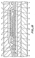
- Figures 1A and 1B together show a cross- sectional side view of a thin film magnetic head in accordance with the invention; and
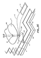
- Figures 2A through 2C together show an exploded perspective view of a thin film magnetic head in accordance with the invention.
- With reference to the drawings, a thin film magnetic head is made by first preparing a
ceramic substrate 30 for deposition thereon of the different layers that form the magnetic head. The ceramic substrate is polished to present a smooth surface on which an insulating layer ofaluminum oxide 20 having a thickness of about 15 micrometers is deposited by r.f. sputtering for example. The insulatingoxide layer 20 is lapped and polished to a thickness of about 12 micrometers to eliminate defects. To form the first pole piece P1, a nickel alloy having about 81% nickel and 19% iron is deposited by r.f. sputtering to a thickness of about 1 x 10⁻⁷ m (1,000 A) over the entire substrate. A mask is used with standard photolithographic processes to form the pattern of the bottom pole piece P1 and anadjoining interconnect layer 13. Thelayer 13 connects a bonding pad A, which is formed at a later process step, to oneend 31 of a first orlower coil 6 of a coil assembly. The P1 pole piece and theinterconnect layer 13 are then plated to the desired thickness. Following another masking sequence, undesired NiFe in the field as well as the seed layer are removed using a standard etching process. - After deposition of the first pole piece P1, a transducing
gap 4 is formed by deposition of a thin layer of aluminum oxide, which may be 0.25x10⁻³ mm to 1×10⁻³ mm (10 to 40 microinches) thick. The aluminum oxide is deposited over the entire surface of the P1 pole piece layer. The portion of the aluminum oxide in the area of theback gap 3, and at the via 14a formed ininterconnect 13, and thevia 24 at the bonding pad A is removed by standard masking and etching steps. - A
first insulation layer 9 is then deposited. The insulation may be formed by baking and hardening the photoresist layer used to define the geometric pattern of the insulation layer. Theinsulation layer 9 is made slightly larger than the pattern of the coil assembly to be deposited, and is opened at via 14a of theinterconnect 13 and via 23 of theback gap closure 3, so thatvias 25 and 14b respectively are formed to allow the necessary interconnections.Insulation layer 9 also serves as a smoothing layer fabricated after forming the pole piece P1 and the interconnects for the coil assembly. - The first or
lower layer 6 of spiral coil turns of the coil assembly is fabricated by first depositing a seed layer, which may be a layer of titanium or chromium about 0.5x10⁻⁷ m―1×10⁻⁷ m (500―1,000 Å) thick on which a copper layer about 1x10⁻⁷ m (1,000 A) thick is deposited by r.f. sputtering. The titanium or chromium acts as an adhesion layer for the copper. The lower coil pattern is defined by photolithography, in a well known manner and the coil is plated to a thickness of about two to three micrometers. The photoresist is then stripped off and the seed layer is removed by chemical etching, ion milling or back sputtering, thereby leaving the desired pattern oflower coil 6. One end of thecoil 6 begins at interconnect 13, via 14a and the other end of thecoil 6 is connected through via 15 tocoil end 33. - The
second insulation layer 10 is then fabricated similarly to thefirst insulation layer 9, but is made slightly smaller than the first insulation layer in order to provide a proper gentle slope at the edges of the layer. Theinsulation layer 10 covers thecoil 6, except at the location ofvia 15 and theback gap closure 3. - A second or
central layer 7 of coil turns is then deposited, in a manner similar to thefirst coil 6. - However, the
second coil layer 7 is formed as a bifilar structure, so that the coil assembly may be used as a center-tapped device. - A
third insulation layer 11 is then deposited to cover thecentral bifilar coil 7 and all other lower structures, excepting theback closure 3 and via 16a, via 18a and via 19a. - A third or
upper layer 8 of coil turns is fabricated in the same manner as described with respect tocoil 6 andcoil 7.Insulation layer 12 is then deposited over the entire coil structure, excepting for theback closure 3, via 16b and via 18b. The upper pole piece P2 is then fabricated together withinterconnect 17 which is made of the same Permalloy material as pole piece P2, and connected to bonding pad B, which is formed at a later step. - Bonding pads A, B and C are plated by a photoresist process with copper, by way of example, to a height substantially above the highest point of the magnetic yoke structure, which is about 40 micrometers in this embodiment. The thin film head is then completed by encapsulating the entire structure with a relatively thick aluminum
oxide insulating layer 21, which is r.f. sputter deposited to a thickness of about 40-45 micrometers. Theovercoat layer 21 provides structural strength to the magnetic structure and protection during machining of the air bearing slider associated with the thin film transducer and during lapping for obtaining the proper desired throat height. - During r.f. sputtering of the aluminum
oxide overcoat layer 21, the copper studs or bonding pads A, B and C are covered. Therefore, the structure is put through a lapping process to reexpose the copper bonding pads for connection to electrical circuitry. To facilitate bonding of wires to the copper pads, the copper is coated with gold to a thickness of about 3-5 micrometers. - With reference to Figs. 2A-:-2C, circuit connection for a continuous flow path for current through the coil assembly is accomplished by alignment of the vias and interconnects formed with the coils and interposed layers allowing coupling of the coils to bonding pads A, B, C for further connection to external circuitry. To this end, the
inner terminal 31 ofcoil 6 is connected withinterconnect 13 through vias 14a and 14b. Theouter end 32 of thelower coil 6 is coupled to theouter terminal 33 of the bifilar coil portion 7a through via 15 ofinsulation layer 10. Theinner end 34 of coil portion 7a is coupled to bonding pad B through via 16a in theinsulation layer 11, via 16b in theinsulation layer 12, and the inner end 16c of theinterconnect 17 which is joined to bonding pad B. The connection from coil portion 7b at itsinner end 36 is made through via 19a formed in theinsulation layer 11 and to theinner terminal 38 of theupper coil 8, while the outer end of coil portion 7b is connected by theinterconnect 35 to bonding pad B through via 35a, via 18a ofinsulation layer 11, via 18b ofinsulation layer 12, and portion 18c of theinterconnect 17. Coupling between the pole pieces P1 and P2 is provided through alignedvias 23 formed by the A1203 gap layer in the P1 pole piece, via 25 in thefirst insulation layer 9, via 26 in thesecond insulation layer 10, via 27 in thethird insulation layer 11, via 28 in thefourth insulation layer 12 andportion 29 in pole piece'P2. - The outer leg of the
upper coil 8 is joined to theinterconnect 42 which leads to bonding pad C. The bonding pads in turn are connected through electrical contacts and leads to external circuitry for processing data signals directed to and from the record medium. - It should be noted that for simplicity and convenience, the drawings show a limited number of coil turns. In a preferred implementation, the upper and lower coils each have eleven turns and the central bifilar coil has five turns in each portion (a total of ten), making a complete three layer coil configuration of 32 turns. For symmetry and balance, the total number of turns of the three coils is an even number.
- There has been disclosed herein a thin film magnetic head having a coil assembly which is characterized by symmetry and which gives increased signal amplitude. The three coil arrangement including a central bifilar coil which has one portion connected to the lower coil and the other portion connected to the upper coil ensures an electrical and magnetic field balance. Positive and negative transitions respectively are processed separately by one portion of the bifilar coil in conjunction with one adjacent coil, and by the second portion of the bifilar coil in conjunction with the other adjacent coil.
Claims (8)
Priority Applications (1)
| Application Number | Priority Date | Filing Date | Title |
|---|---|---|---|
| AT87300200T ATE54034T1 (en) | 1986-01-10 | 1987-01-09 | THIN FILM MAGNETIC HEAD. |
Applications Claiming Priority (2)
| Application Number | Priority Date | Filing Date | Title |
|---|---|---|---|
| US06/817,621 US4694368A (en) | 1986-01-10 | 1986-01-10 | Thin film magnetic head with three superimposed coils |
| US817621 | 1986-01-10 |
Publications (2)
| Publication Number | Publication Date |
|---|---|
| EP0234689A1 EP0234689A1 (en) | 1987-09-02 |
| EP0234689B1 true EP0234689B1 (en) | 1990-06-20 |
Family
ID=25223479
Family Applications (1)
| Application Number | Title | Priority Date | Filing Date |
|---|---|---|---|
| EP87300200A Expired - Lifetime EP0234689B1 (en) | 1986-01-10 | 1987-01-09 | Thin film magnetic head |
Country Status (5)
| Country | Link |
|---|---|
| US (1) | US4694368A (en) |
| EP (1) | EP0234689B1 (en) |
| JP (1) | JPS62264413A (en) |
| AT (1) | ATE54034T1 (en) |
| DE (1) | DE3763348D1 (en) |
Families Citing this family (12)
| Publication number | Priority date | Publication date | Assignee | Title |
|---|---|---|---|---|
| JPH02122410A (en) * | 1988-10-31 | 1990-05-10 | Yamaha Corp | Thin film magnetic head |
| JPH0413212A (en) * | 1990-05-07 | 1992-01-17 | Mitsubishi Electric Corp | Thin-film magnetic head |
| US5472736A (en) * | 1991-06-03 | 1995-12-05 | Read-Rite Corporation | Method of making a bi-level coil for a thin film magnetic transducer |
| US5875080A (en) * | 1997-09-05 | 1999-02-23 | International Business Machines Corporation | Write head with second coil above pole having coil density less electrically connected first coil below the pole |
| US6483662B1 (en) | 1999-07-09 | 2002-11-19 | Read-Rite Corporation | High density multi-coil magnetic write head having a reduced yoke length and short flux rise time |
| US6496330B1 (en) | 1999-09-09 | 2002-12-17 | Read-Rite Corporation | Magnetic write head having a splitcoil structure |
| US6621660B2 (en) * | 2001-01-16 | 2003-09-16 | International Business Machines Corporation | Thin film magnetic head |
| US6560864B1 (en) * | 2001-11-14 | 2003-05-13 | Headway Technologies, Inc. | Process for manufacturing a flat coil |
| US8797684B1 (en) | 2011-12-20 | 2014-08-05 | Western Digital (Fremont), Llc | Magnetic writer configured for high data rate recording |
| US8786983B1 (en) | 2012-06-25 | 2014-07-22 | Western Digital (Fremont), Llc | Magnetic writer having a low aspect ratio two layer coil |
| US9245545B1 (en) | 2013-04-12 | 2016-01-26 | Wester Digital (Fremont), Llc | Short yoke length coils for magnetic heads in disk drives |
| US9196275B1 (en) | 2014-03-12 | 2015-11-24 | Western Digital Technologies, Inc. | Magnetic head separator fin material to prevent particulate contamination on slider |
Family Cites Families (10)
| Publication number | Priority date | Publication date | Assignee | Title |
|---|---|---|---|---|
| US3685144A (en) * | 1967-09-18 | 1972-08-22 | Ncr Co | Method of making a magnetic transducer |
| US3945038A (en) * | 1971-12-22 | 1976-03-16 | Compagnie Internationale Pour L'informatique | Read-write magnetoresistive transducer having a plurality of MR elements |
| JPS51117020A (en) * | 1975-04-07 | 1976-10-14 | Hitachi Ltd | Magnetic head and production method of it |
| FR2455330A1 (en) * | 1979-04-25 | 1980-11-21 | Cii Honeywell Bull | MAGNETIC RESISTANCE TRANSDUCTION DEVICE |
| JPS5616932A (en) * | 1979-07-18 | 1981-02-18 | Olympus Optical Co Ltd | Recording and reproducing head for vertical magnetic recording and manufacture of this recording and reproducing head and recording and reproducing unit using this recording and reproducing head |
| US4295173A (en) * | 1979-10-18 | 1981-10-13 | International Business Machines Corporation | Thin film inductive transducer |
| FR2468183A1 (en) * | 1979-10-25 | 1981-04-30 | Cii Honeywell Bull | INTEGRATED MAGNETIC TRANSDUCER |
| US4343026A (en) * | 1980-07-09 | 1982-08-03 | Spin Physics, Inc. | Magnetoresistive head employing field feedback |
| JPS5850013A (en) * | 1981-09-18 | 1983-03-24 | Toyota Motor Corp | Constant-speed running device for vehicle |
| US4593334A (en) * | 1983-05-02 | 1986-06-03 | International Business Machines Corporation | Thin film transducer |
-
1986
- 1986-01-10 US US06/817,621 patent/US4694368A/en not_active Expired - Fee Related
-
1987
- 1987-01-09 DE DE8787300200T patent/DE3763348D1/en not_active Expired - Fee Related
- 1987-01-09 AT AT87300200T patent/ATE54034T1/en not_active IP Right Cessation
- 1987-01-09 EP EP87300200A patent/EP0234689B1/en not_active Expired - Lifetime
- 1987-01-09 JP JP62003083A patent/JPS62264413A/en active Pending
Also Published As
| Publication number | Publication date |
|---|---|
| US4694368A (en) | 1987-09-15 |
| ATE54034T1 (en) | 1990-07-15 |
| JPS62264413A (en) | 1987-11-17 |
| EP0234689A1 (en) | 1987-09-02 |
| DE3763348D1 (en) | 1990-07-26 |
Similar Documents
| Publication | Publication Date | Title |
|---|---|---|
| EP0131716B1 (en) | Composite thin film transducer head | |
| US5995342A (en) | Thin film heads having solenoid coils | |
| EP0234689B1 (en) | Thin film magnetic head | |
| US5173826A (en) | Thin film head with coils of varying thickness | |
| US6034848A (en) | Low profile multi-layer coil merged thin film magnetic head | |
| JPS638527B2 (en) | ||
| JPH0628626A (en) | Thin-film magnetic head and its manufacture | |
| JP2001118216A (en) | Magnetic writing head having divided coil structure, thin-film magnetic writing head and its manufacturing method | |
| JP2003030803A (en) | Magnetic head assembly and its manufacturing method | |
| JP3345588B2 (en) | Thin film magnetic head and method of manufacturing the same | |
| EP0514600B1 (en) | Thin film transducer/transformer assembly | |
| JPH07201010A (en) | Magnetic head and its production | |
| US7336445B2 (en) | Conductive stud for magnetic recording devices and method of making the same | |
| JP2002343639A (en) | Thin-film coil, magnet head, method of manufacturing the coil, and method of manufacturing the head | |
| US5312644A (en) | Method of making a magnetoresistive head with integrated bias and magnetic shield layer | |
| KR0178305B1 (en) | Process for forming vertical gap in a thin film magnetic transducer | |
| JPS59195311A (en) | Vertical magnetic head | |
| JPS58118017A (en) | Magnetic head | |
| JP2000195016A (en) | Thin film magnetic head | |
| JPH05114116A (en) | Integrated magnetic lead/writing head/ flexible body/conductor structure | |
| JPH04356707A (en) | Thin film magnetic head | |
| JPH08287407A (en) | Composite type magnetic head and its production | |
| JPH11191203A (en) | Magnetic head and manufacture therefor | |
| JPH07311917A (en) | Thin film magnetic head | |
| JP2551749B2 (en) | Method of manufacturing thin film magnetic head |
Legal Events
| Date | Code | Title | Description |
|---|---|---|---|
| PUAI | Public reference made under article 153(3) epc to a published international application that has entered the european phase |
Free format text: ORIGINAL CODE: 0009012 |
|
| AK | Designated contracting states |
Kind code of ref document: A1 Designated state(s): AT BE CH DE ES FR GB GR IT LI LU NL SE |
|
| 17P | Request for examination filed |
Effective date: 19880114 |
|
| 17Q | First examination report despatched |
Effective date: 19890623 |
|
| GRAA | (expected) grant |
Free format text: ORIGINAL CODE: 0009210 |
|
| AK | Designated contracting states |
Kind code of ref document: B1 Designated state(s): AT BE CH DE ES FR GB GR IT LI LU NL SE |
|
| PG25 | Lapsed in a contracting state [announced via postgrant information from national office to epo] |
Ref country code: SE Effective date: 19900620 Ref country code: NL Effective date: 19900620 Ref country code: GR Free format text: LAPSE BECAUSE OF FAILURE TO SUBMIT A TRANSLATION OF THE DESCRIPTION OR TO PAY THE FEE WITHIN THE PRESCRIBED TIME-LIMIT Effective date: 19900620 |
|
| REF | Corresponds to: |
Ref document number: 54034 Country of ref document: AT Date of ref document: 19900715 Kind code of ref document: T |
|
| REF | Corresponds to: |
Ref document number: 3763348 Country of ref document: DE Date of ref document: 19900726 |
|
| ET | Fr: translation filed | ||
| ITF | It: translation for a ep patent filed |
Owner name: FUMERO BREVETTI S.N.C. |
|
| PG25 | Lapsed in a contracting state [announced via postgrant information from national office to epo] |
Ref country code: ES Free format text: LAPSE BECAUSE OF FAILURE TO SUBMIT A TRANSLATION OF THE DESCRIPTION OR TO PAY THE FEE WITHIN THE PRESCRIBED TIME-LIMIT Effective date: 19901001 |
|
| NLV1 | Nl: lapsed or annulled due to failure to fulfill the requirements of art. 29p and 29m of the patents act | ||
| PGFP | Annual fee paid to national office [announced via postgrant information from national office to epo] |
Ref country code: GB Payment date: 19901228 Year of fee payment: 5 |
|
| PGFP | Annual fee paid to national office [announced via postgrant information from national office to epo] |
Ref country code: CH Payment date: 19910111 Year of fee payment: 5 |
|
| PGFP | Annual fee paid to national office [announced via postgrant information from national office to epo] |
Ref country code: BE Payment date: 19910115 Year of fee payment: 5 |
|
| PGFP | Annual fee paid to national office [announced via postgrant information from national office to epo] |
Ref country code: FR Payment date: 19910130 Year of fee payment: 5 Ref country code: AT Payment date: 19910130 Year of fee payment: 5 |
|
| ITTA | It: last paid annual fee | ||
| PG25 | Lapsed in a contracting state [announced via postgrant information from national office to epo] |
Ref country code: LU Free format text: LAPSE BECAUSE OF NON-PAYMENT OF DUE FEES Effective date: 19910131 |
|
| PGFP | Annual fee paid to national office [announced via postgrant information from national office to epo] |
Ref country code: DE Payment date: 19910320 Year of fee payment: 5 |
|
| PLBE | No opposition filed within time limit |
Free format text: ORIGINAL CODE: 0009261 |
|
| STAA | Information on the status of an ep patent application or granted ep patent |
Free format text: STATUS: NO OPPOSITION FILED WITHIN TIME LIMIT |
|
| 26N | No opposition filed | ||
| PG25 | Lapsed in a contracting state [announced via postgrant information from national office to epo] |
Ref country code: GB Effective date: 19920109 Ref country code: AT Effective date: 19920109 |
|
| PG25 | Lapsed in a contracting state [announced via postgrant information from national office to epo] |
Ref country code: LI Effective date: 19920131 Ref country code: CH Effective date: 19920131 Ref country code: BE Effective date: 19920131 |
|
| BERE | Be: lapsed |
Owner name: READ-RITE CORP. Effective date: 19920131 |
|
| GBPC | Gb: european patent ceased through non-payment of renewal fee | ||
| PG25 | Lapsed in a contracting state [announced via postgrant information from national office to epo] |
Ref country code: FR Effective date: 19920930 |
|
| REG | Reference to a national code |
Ref country code: CH Ref legal event code: PL |
|
| PG25 | Lapsed in a contracting state [announced via postgrant information from national office to epo] |
Ref country code: DE Effective date: 19921001 |
|
| REG | Reference to a national code |
Ref country code: FR Ref legal event code: ST |
|
| PG25 | Lapsed in a contracting state [announced via postgrant information from national office to epo] |
Ref country code: IT Free format text: LAPSE BECAUSE OF NON-PAYMENT OF DUE FEES;WARNING: LAPSES OF ITALIAN PATENTS WITH EFFECTIVE DATE BEFORE 2007 MAY HAVE OCCURRED AT ANY TIME BEFORE 2007. THE CORRECT EFFECTIVE DATE MAY BE DIFFERENT FROM THE ONE RECORDED. Effective date: 20050109 |