EP0232427A1 - Optical recording medium - Google Patents
Optical recording medium Download PDFInfo
- Publication number
- EP0232427A1 EP0232427A1 EP86904931A EP86904931A EP0232427A1 EP 0232427 A1 EP0232427 A1 EP 0232427A1 EP 86904931 A EP86904931 A EP 86904931A EP 86904931 A EP86904931 A EP 86904931A EP 0232427 A1 EP0232427 A1 EP 0232427A1
- Authority
- EP
- European Patent Office
- Prior art keywords
- group
- optical recording
- recording member
- substituted
- member according
- Prior art date
- Legal status (The legal status is an assumption and is not a legal conclusion. Google has not performed a legal analysis and makes no representation as to the accuracy of the status listed.)
- Granted
Links
Classifications
-
- G—PHYSICS
- G11—INFORMATION STORAGE
- G11B—INFORMATION STORAGE BASED ON RELATIVE MOVEMENT BETWEEN RECORD CARRIER AND TRANSDUCER
- G11B7/00—Recording or reproducing by optical means, e.g. recording using a thermal beam of optical radiation by modifying optical properties or the physical structure, reproducing using an optical beam at lower power by sensing optical properties; Record carriers therefor
- G11B7/24—Record carriers characterised by shape, structure or physical properties, or by the selection of the material
- G11B7/241—Record carriers characterised by shape, structure or physical properties, or by the selection of the material characterised by the selection of the material
- G11B7/242—Record carriers characterised by shape, structure or physical properties, or by the selection of the material characterised by the selection of the material of recording layers
- G11B7/244—Record carriers characterised by shape, structure or physical properties, or by the selection of the material characterised by the selection of the material of recording layers comprising organic materials only
- G11B7/246—Record carriers characterised by shape, structure or physical properties, or by the selection of the material characterised by the selection of the material of recording layers comprising organic materials only containing dyes
- G11B7/248—Record carriers characterised by shape, structure or physical properties, or by the selection of the material characterised by the selection of the material of recording layers comprising organic materials only containing dyes porphines; azaporphines, e.g. phthalocyanines
-
- Y—GENERAL TAGGING OF NEW TECHNOLOGICAL DEVELOPMENTS; GENERAL TAGGING OF CROSS-SECTIONAL TECHNOLOGIES SPANNING OVER SEVERAL SECTIONS OF THE IPC; TECHNICAL SUBJECTS COVERED BY FORMER USPC CROSS-REFERENCE ART COLLECTIONS [XRACs] AND DIGESTS
- Y10—TECHNICAL SUBJECTS COVERED BY FORMER USPC
- Y10S—TECHNICAL SUBJECTS COVERED BY FORMER USPC CROSS-REFERENCE ART COLLECTIONS [XRACs] AND DIGESTS
- Y10S430/00—Radiation imagery chemistry: process, composition, or product thereof
- Y10S430/146—Laser beam
Definitions
- This invention relates to an optical recording member containing phthalocyanine type coloring matter in its information recording layer.
- the invention is concerned with such optical recording member that performs recording of information utilizing changes in the state of substance due to light energy having an oscillating wavelength of a semiconductor laser.
- optical disc As one example of such optical recording, there may be mentioned an optical disc.
- the optical disc carries out high density recording of information by irradiation of laser beam which has been collimated to a beam diameter of 1 ⁇ m or so onto a thin recording layer provided on a circular base member.
- the information recording is effected by thermal deformation of the recording layer such as its decomposition, evaporation, dissolution, and others which take place at particular portions of the recording layer owing to its absorption of the laser energy as irradiated onto it.
- the reproduction of the recorded information is done by reading of a difference in the reflection factor between the portion where the deformation has taken place by the laser beam and the portion where no deformation has occurred.
- the recording member therefore, it is necessary to have high absorptivity to the laser beam of a particular wavelength to be used for the recording, because the recording member is required to absorb energy of the laser beam with good efficiency, and also to have high reflection factor to the laser beam of a particular wavelength for use in the reproduction so as to carry out the accurate reproduction of the recorded information.
- inorganic compounds such as metals, metal compounds, chalcogenides, and so on.
- the thin films made of these inorganic compounds have various disadvantages such that they are susceptible to oxidation in the air, difficult to preserve over a long period of time, sensitive to the ultraviolet part or the visible part of the light rays, not durable against the sun light and other lights, and so forth.
- the organic compounds to be used for the recording member there have so far been proposed cyanine type coloring matter, squalerium type coloring matter, naphthoquinone type coloring matter, phthalocyanine type coloring matter, and so on.
- the phthalocyanine type coloring matter is highly stable to the ultraviolet part and the visible part of the light rays, while it is remarkably inferior in its solubility to organic solvents, hence it has a shortcoming such that the economically advantageous coating method cannot be adopted for the thin film forming.
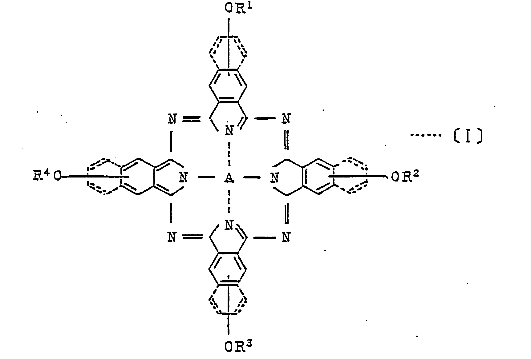
- the present invention has its gist in an optical recording member comprising a substrate; and a recording layer which contains therein a light absorbing substance to be represented by the following general formula [I]:
- General Formula [I] (where: R 1 , R 2 , R 3 and R represent the alkyl group having C 1 to C 22 which may be substituted, or or (x denoting halogen atom; Y representing hydrogen atom, aryl group, or alkyl group which may be substituted; n indicating an integer of from 1 to 4; m indicating an integer of 0, 1 or 2; and Z denotig hydrogen atom, carboxylic acid group, carboxylic acid ester group, aryl group, alkyl group which may be substituted, or alkoxy group which may be substituted); and A represents metals belonging to I-B group, II-A group, II-B group, III-A group, III-B group, IV-A group, IV-B group, V-B group and VIII group of the Periodic Table, or compounds containing
- the compound to be used as the light absorbing substance for the optical recording member according to the present invention is represented by the above general formula [I].
- the halogen atom represented by X in this light absorbing substance of the above-mentioned general formula [I] there may be exemplified fluorine, chlorine, bromine, iodine, and so forth;
- Y there may be enumerated hydrogen, aryl group such as phenyl group, etc., or alkyl group having C 1 to C 25 which may be substituted by hydroxyl group, carboxylic acid group or carboxylic acid ester group, among them, lower alkyl group having C 1 to C 4 such as methyl, ethyl, butyl, etc.
- Z there may be enumerated hydrogen; carboxylic acid; carboxylic acid ester group; aryl group such as phenyl group, etc.;.alkyl group having C 1 to C 25 which may be substituted by hydroxyl group, phenyl group, carboxylic acid group or carboxylic acid ester group; and alkoxy group which may be substituted by alkoxy group, alkoxy-alkoxy group, or alkoxy-alkoxy-alkoxy group, and so forth.
- substituent group of the alkyl group having C 1 to C 22 and which may be substituted by those groups as represented by R l , R 2 , R 3 and R 4 there may be exemplified hydroxyl group, carboxylic acid group or carboxylic acid ester group, and so on.
- the metals for A belonging to I-B group, II-A group, III-A group, III-B group, IV-A group, IV-B group, V-B group and VIII group of the Periodic Table there are Cu, Mg, Zn, Ge, Sn, Si, Pb, Fe, Co and Ni.
- the compounds containing such metals there are A1C1, InCl, TiO, VO, GeCl 2 , SnCl 2 , SnBr 2 , SnF 2 , SnI 2 and so on.
- R 1 , R 2 , R 3 and R4 should preferably be lower alkoxy lower alkyl group. Concrete examples of these are methoxy ethyl group and butoxy ethyl group.
- the examples of A should preferably be VO, Ni and Cu. Among them VO is particularly favorable.
- R has the same definition for R l , R 2 , R 3 or R 4 mentioned above.
- the material for the base plate according to the present invention there may be exemplified glass, plastics, and so forth. Of these various substrate materials, plastics is preferable from the standpoint of its stability and light weight. Examples of the plastics are: acrylic resin, methacrylic resin, polycarbonate resin, vinyl chloride resin, vinyl acetate resin, polyester resin, polyethylene resin, polypropylene resin, polyamide resin, polystyrene resin, epoxy resin, and so forth.
- the film forming method for the recording layer there may be enumerated various known methods such as vacuum deposition of the thin film on the base plate; mixing of the thin film material with a resin solution and applying the mixed solution on the base plate; dissolution of the thin film material in a solvent and coating the solution on the base plate; or immersing the base plate into the coating liquid; and others.
- the compound of the present invention is suited for the coating method, since it has good solubility to the solvent.
- the film forming by the application of the coating liquid may be attained by dissolving the compound as represented by the foregoing general formula [1] as the light absorbing substance into a solvent, for instance, with addition of a binder, as the case may be, and spin-coating the coating liquid onto the base plate.
- a binder there may be exemplified polyimide resin, polyamide resin, polystyrene resin, acrylic resin, polyester resin, polycarbonate resin, cellulosic resin, and so forth.
- a ratio of such light absorbing substance to the resin should desirably be 10 % by weight or above.
- the solvent there may be used dimethyl formamide, methyl ethyl ketone, methylcellosolve, ethanol, tetrahydrofuran, dichloromethane, chlorobenzene, and various others.
- the recording layer for the optical recording member according to the present invention may be provided on both surfaces of the base plate or on one surface thereof.
- Recording of information onto the recording member which has been obtained in the above-described manner is effected by irradiating a laser beam, preferably a semiconductor laser beam collimated to a beam diameter of 1 ⁇ m or so onto the recording layer provided on both surfaces or one surface of the substrate. Those portions of the recording layer irradiated by the laser beam bring about thermal deformation such as decomposition, evaporation, fusion, etc. owing to its absorption of the laser energy.
- a laser beam preferably a semiconductor laser beam collimated to a beam diameter of 1 ⁇ m or so onto the recording layer provided on both surfaces or one surface of the substrate.
- Reproduction of the recorded information is done by reading of a difference in the reflection factor between the portion where the thermal deformation has occurred by the laser beam and the portion where such thermal deformation has not taken place.
- the light source various lasers such as He-Ne laser, Ar laser, semiconductor laser, etc. may be used.
- the semiconductor laser is particularly preferable in respect of the price and the size of the laser device.
- the semiconductor laser to be used may have its central wavelength of 830 nm, 780 nm, and a wavelenght shorter than these.
- o.4 g of o-dicyano compound to be represented by the following structural formula: and 0.25 g of PbO were mixed and melted at an elevated temperature of 210°C under a reduced pressure, and then the molten mixture was agitated at this temperature level for 14 hours.
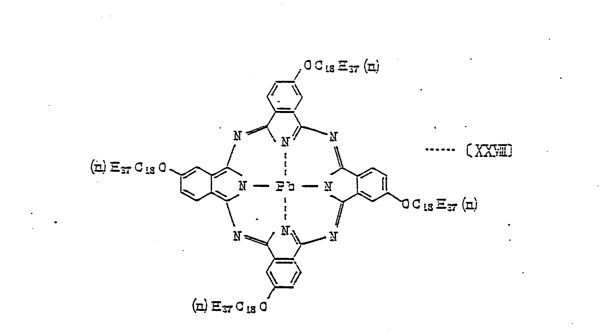
- the thus obtained crude crystals were refined by a column chromatography to obtain 0.18 g of dark blue crystals of the light absorbing substance according to the present invention (m.p. 243 0 C to 244°C) as represented by the following general formula [III].
- the maximum absorbing wavelength ⁇ max of this substance in the chloroform solvent was 723 nm.
- the light absorbing substance of the present invention as represented by the above formula [III] was dissolved into methyl ethyl ketone, and the solution was coated onto the base plate of methacrylic resin by the spin-coating technique (at the number of revolution of 2,000 rpm) to obtain a thin film of 2,500 A thick.
- the maximum absorbing wavelength of this thin film was 730 nm, indicating that it had a broad peak.
- the semiconductor laser beam having its central wavelength of 780 nm was irradiated with a beam diameter of about 1 ⁇ m and an output of 4 mW, whereupon pits of very clear and distinct profile, each having a width of about 1 ⁇ m and a pit length of about 2 ⁇ m were formed.
- the C/N (carrier level/ noise level) ratio thereof was 52 dB.
- Table 1 below indicates the writing performance (C/N ratio) of this thin film by the semiconductor laser, after the same was preserved for ten days in a constant temperature and humidity vessel at 60°C and 80 % (of relative humidity).
- the light absorbing substances of the present invention represented by the following formulas [IV] to [XXXVI], and synthesized in accordance with Example 1 above were each formed into their respective films on an individual base plate of methacrylic resin under the substantially same conditions as in Example 1 above.
- Table 1 shows, along with the results of Example 1 above, the maximum absorbing wavelength, the C/N ratio at the time of recording by the semiconductor laser, and the storage stability of the thin films of the light absorbing substances according to the present invention.
- the storage stability thereof is shown in terms of the writing performance (C/N ratio) by the semiconductor laser, after the thin films were preserved for ten days in a constant temperature and humidity vessel at 60°C and 80 % (of relative humidity).
- 0.2 g of the light absorbing substance according to the present invention as represented by the formula [III] was dissolved into 10 % of methyl ethyl ketone, and then 1 g of nitrocellulose solution (manufactured by Dicel K.K., Japan: 25 % by weight solution of methyl ethyl ketone) as a binder was added to be dissolved into it.
- the solution was coated on the base plate of methacrylic resin by the spin-coating technique (at the number of 0 revolution of 1,500 rpm) to obtain a thin film of 1,200 A thick.
- the maximum absorbing wavelength of this thin film was 730 nm, which indicates that it had a broad peak.
- the semiconductor laser beam having its central wavelength of 780 nm was irradiated with a beam diameter of about 1 ⁇ m at an output of 4 mW, whereupon pits of very clear and distinct profiles, each having a width of about 1 ⁇ m and a pit length of about 2 ⁇ m were formed.
- the C/N (carrier level/noise level) ratio thereof was 53 dB.
- the writing performance (C/N ratio) of this thin film by the semiconductor laser after the same was preserved for ten days in a constant temperature and humidity vessel at 60°C and 80 % (of relative humidity) was 53 dB.
- 0.2 g of the light absorbing substance according to the present invention as represented by the formula [III] was dissolved into 10 g of methyl ethyl ketone, and then 0.2 g of acetyl cellulose ("L-20" - manufactured by Dicel K.K., Japan) as a binder was added to be dissolved into it.
- the solution was coated on the base plate of methacrylic resin by the spin-coating technique (at the number of revolution of 1,500 rpm) to obain a thin film 0 of 1,500 A thick.
- the maximum absorbing wavelength of this thin film was 730 nm, which indicates that it had a broad peak.
- the semiconductor laser beam having its central wavelength of 780 nm was irradiated with a beam diameter of about 1 ⁇ m at an output of 4 mW, whereupon pits of very clear and distinct profiles, each having a width of about 1 ⁇ m and a pit length of about 2 ⁇ m were formed.
- the C/N (carrier level/noise level) ratio thereof was 52 dB.
- the optical recording member of the present invention can also be manufactured by the coating method, in which the light absorbing substance is applied onto the base plate.
- the obtained optical recording member according to the present invention has high reflection factor, on account of which its contrast is satisfactory as indicated by the C/N ratio, with the consequence that the information recorded in the optical recording member can be easily and clearly reproduced.
Landscapes
- Thermal Transfer Or Thermal Recording In General (AREA)
- Optical Record Carriers And Manufacture Thereof (AREA)
Abstract
Description
- This invention relates to an optical recording member containing phthalocyanine type coloring matter in its information recording layer.
- More specifically, the invention is concerned with such optical recording member that performs recording of information utilizing changes in the state of substance due to light energy having an oscillating wavelength of a semiconductor laser.
- Development in the optical recording which utilizes the laser technology has been desired particularly in recent years owing to its capability of preservation and reproduction of,information recorded in high density.
- As one example of such optical recording, there may be mentioned an optical disc.
- In general, the optical disc carries out high density recording of information by irradiation of laser beam which has been collimated to a beam diameter of 1 µm or so onto a thin recording layer provided on a circular base member.
- The information recording is effected by thermal deformation of the recording layer such as its decomposition, evaporation, dissolution, and others which take place at particular portions of the recording layer owing to its absorption of the laser energy as irradiated onto it. On the other hand, the reproduction of the recorded information is done by reading of a difference in the reflection factor between the portion where the deformation has taken place by the laser beam and the portion where no deformation has occurred.
- For the recording member, therefore, it is necessary to have high absorptivity to the laser beam of a particular wavelength to be used for the recording, because the recording member is required to absorb energy of the laser beam with good efficiency, and also to have high reflection factor to the laser beam of a particular wavelength for use in the reproduction so as to carry out the accurate reproduction of the recorded information.
- For such optical recording member, there have so far been proposed various inorganic compounds such as metals, metal compounds, chalcogenides, and so on. However, the thin films made of these inorganic compounds have various disadvantages such that they are susceptible to oxidation in the air, difficult to preserve over a long period of time, sensitive to the ultraviolet part or the visible part of the light rays, not durable against the sun light and other lights, and so forth.
- As the organic compounds to be used for the recording member, there have so far been proposed cyanine type coloring matter, squalerium type coloring matter, naphthoquinone type coloring matter, phthalocyanine type coloring matter, and so on. Of these various coloring matters, the phthalocyanine type coloring matter is highly stable to the ultraviolet part and the visible part of the light rays, while it is remarkably inferior in its solubility to organic solvents, hence it has a shortcoming such that the economically advantageous coating method cannot be adopted for the thin film forming.
- It is an object of the present invention to provide an optical recording member of an organic substance which has high sensitivity to writing by the laser beam, particularly the semiconductor laser beam, has good stability in its preservation, and yet, is capable of forming the thin film by the coating method.
- The present invention has its gist in an optical recording member comprising a substrate; and a recording layer which contains therein a light absorbing substance to be represented by the following general formula [I]: General Formula [I]


- The compound to be used as the light absorbing substance for the optical recording member according to the present invention is represented by the above general formula [I]. For the halogen atom represented by X in this light absorbing substance of the above-mentioned general formula [I], there may be exemplified fluorine, chlorine, bromine, iodine, and so forth; for Y, there may be enumerated hydrogen, aryl group such as phenyl group, etc., or alkyl group having C1 to C25 which may be substituted by hydroxyl group, carboxylic acid group or carboxylic acid ester group, among them, lower alkyl group having C1 to C4 such as methyl, ethyl, butyl, etc. is preferable; for Z, there may be enumerated hydrogen; carboxylic acid; carboxylic acid ester group; aryl group such as phenyl group, etc.;.alkyl group having C1 to C25 which may be substituted by hydroxyl group, phenyl group, carboxylic acid group or carboxylic acid ester group; and alkoxy group which may be substituted by alkoxy group, alkoxy-alkoxy group, or alkoxy-alkoxy-alkoxy group, and so forth. For the substituent group of the alkyl group having C1 to C22 and which may be substituted by those groups as represented by Rl, R2, R3 and R4, there may be exemplified hydroxyl group, carboxylic acid group or carboxylic acid ester group, and so on.
- As the example of the metals for A belonging to I-B group, II-A group, III-A group, III-B group, IV-A group, IV-B group, V-B group and VIII group of the Periodic Table, there are Cu, Mg, Zn, Ge, Sn, Si, Pb, Fe, Co and Ni. As the example of the compounds containing such metals, there are A1C1, InCl, TiO, VO, GeCl2, SnCl2, SnBr2, SnF2, SnI2 and so on. In the compound to be represented by the general formula [1], R1, R2, R3 and R4 should preferably be lower alkoxy lower alkyl group. Concrete examples of these are methoxy ethyl group and butoxy ethyl group. Also, the examples of A should preferably be VO, Ni and Cu. Among them VO is particularly favorable.
- These compounds can be easily produced by a known method from o-dicyano compound to be represented by the following general formula [II] and a metal or a metal compound. (vide: for example, "Journal of American Chemical Society, Vol. 106, No. 174706-4711(1984)" - article by A.W. Snow and N.L. Jarvis)

- Where R has the same definition for R l, R 2, R 3 or R 4 mentioned above. As the material for the base plate according to the present invention, there may be exemplified glass, plastics, and so forth. Of these various substrate materials, plastics is preferable from the standpoint of its stability and light weight. Examples of the plastics are: acrylic resin, methacrylic resin, polycarbonate resin, vinyl chloride resin, vinyl acetate resin, polyester resin, polyethylene resin, polypropylene resin, polyamide resin, polystyrene resin, epoxy resin, and so forth.
- As the film forming method for the recording layer, there may be enumerated various known methods such as vacuum deposition of the thin film on the base plate; mixing of the thin film material with a resin solution and applying the mixed solution on the base plate; dissolution of the thin film material in a solvent and coating the solution on the base plate; or immersing the base plate into the coating liquid; and others. In particular, the compound of the present invention is suited for the coating method, since it has good solubility to the solvent.
- The film forming by the application of the coating liquid may be attained by dissolving the compound as represented by the foregoing general formula [1] as the light absorbing substance into a solvent, for instance, with addition of a binder, as the case may be, and spin-coating the coating liquid onto the base plate. As the binder, there may be exemplified polyimide resin, polyamide resin, polystyrene resin, acrylic resin, polyester resin, polycarbonate resin, cellulosic resin, and so forth. In this case, use of a mixture of phthalocyanine type compound and naphthalocyanine type compound out of the coating compounds represented by the foregoing general formula [I] is preferable. A ratio of such light absorbing substance to the resin should desirably be 10 % by weight or above.
- As the solvent, there may be used dimethyl formamide, methyl ethyl ketone, methylcellosolve, ethanol, tetrahydrofuran, dichloromethane, chlorobenzene, and various others.
- The recording layer for the optical recording member according to the present invention may be provided on both surfaces of the base plate or on one surface thereof.
- Recording of information onto the recording member which has been obtained in the above-described manner is effected by irradiating a laser beam, preferably a semiconductor laser beam collimated to a beam diameter of 1 µm or so onto the recording layer provided on both surfaces or one surface of the substrate. Those portions of the recording layer irradiated by the laser beam bring about thermal deformation such as decomposition, evaporation, fusion, etc. owing to its absorption of the laser energy.
- Reproduction of the recorded information is done by reading of a difference in the reflection factor between the portion where the thermal deformation has occurred by the laser beam and the portion where such thermal deformation has not taken place.
- As the light source, various lasers such as He-Ne laser, Ar laser, semiconductor laser, etc. may be used. Among them, the semiconductor laser is particularly preferable in respect of the price and the size of the laser device.
- The semiconductor laser to be used may have its central wavelength of 830 nm, 780 nm, and a wavelenght shorter than these.
- o.4 g of o-dicyano compound to be represented by the following structural formula:


- The light absorbing substance of the present invention as represented by the above formula [III] was dissolved into methyl ethyl ketone, and the solution was coated onto the base plate of methacrylic resin by the spin-coating technique (at the number of revolution of 2,000 rpm) to obtain a thin film of 2,500 A thick. The maximum absorbing wavelength of this thin film was 730 nm, indicating that it had a broad peak.
- To this thin film, the semiconductor laser beam having its central wavelength of 780 nm was irradiated with a beam diameter of about 1 µm and an output of 4 mW, whereupon pits of very clear and distinct profile, each having a width of about 1 µm and a pit length of about 2 µm were formed. The C/N (carrier level/ noise level) ratio thereof was 52 dB. Table 1 below indicates the writing performance (C/N ratio) of this thin film by the semiconductor laser, after the same was preserved for ten days in a constant temperature and humidity vessel at 60°C and 80 % (of relative humidity).
- The light absorbing substances of the present invention represented by the following formulas [IV] to [XXXVI], and synthesized in accordance with Example 1 above were each formed into their respective films on an individual base plate of methacrylic resin under the substantially same conditions as in Example 1 above.
- Table 1 shows, along with the results of Example 1 above, the maximum absorbing wavelength, the C/N ratio at the time of recording by the semiconductor laser, and the storage stability of the thin films of the light absorbing substances according to the present invention. In the Table, the storage stability thereof is shown in terms of the writing performance (C/N ratio) by the semiconductor laser, after the thin films were preserved for ten days in a constant temperature and humidity vessel at 60°C and 80 % (of relative humidity).




- 0.2 g of the light absorbing substance according to the present invention as represented by the formula [III] was dissolved into 10 % of methyl ethyl ketone, and then 1 g of nitrocellulose solution (manufactured by Dicel K.K., Japan: 25 % by weight solution of methyl ethyl ketone) as a binder was added to be dissolved into it. The solution was coated on the base plate of methacrylic resin by the spin-coating technique (at the number of 0 revolution of 1,500 rpm) to obtain a thin film of 1,200 A thick. The maximum absorbing wavelength of this thin film was 730 nm, which indicates that it had a broad peak.
- To this thin film, the semiconductor laser beam having its central wavelength of 780 nm was irradiated with a beam diameter of about 1 µm at an output of 4 mW, whereupon pits of very clear and distinct profiles, each having a width of about 1 µm and a pit length of about 2 µm were formed. The C/N (carrier level/noise level) ratio thereof was 53 dB. The writing performance (C/N ratio) of this thin film by the semiconductor laser after the same was preserved for ten days in a constant temperature and humidity vessel at 60°C and 80 % (of relative humidity) was 53 dB.
- 0.2 g of the light absorbing substance according to the present invention as represented by the formula [III] was dissolved into 10 g of methyl ethyl ketone, and then 0.2 g of acetyl cellulose ("L-20" - manufactured by Dicel K.K., Japan) as a binder was added to be dissolved into it. The solution was coated on the base plate of methacrylic resin by the spin-coating technique (at the number of revolution of 1,500 rpm) to obain a thin film 0 of 1,500 A thick. The maximum absorbing wavelength of this thin film was 730 nm, which indicates that it had a broad peak.
- To this thin film, the semiconductor laser beam having its central wavelength of 780 nm was irradiated with a beam diameter of about 1 µm at an output of 4 mW, whereupon pits of very clear and distinct profiles, each having a width of about 1 µm and a pit length of about 2 µm were formed. The C/N (carrier level/noise level) ratio thereof was 52 dB.
- The writing performance (C/N ratio) of this thin film by the semiconductor laser after the same was preserved for ten days in a constant temperature and humidity vessel at 60°C and 80 % (of relative humidity) was 52 dB.
- Besides the method of producing it by the evaporative deposition of phthalocyanine type coloring matter represented by a particular strucutral formula onto the base plate, the optical recording member of the present invention can also be manufactured by the coating method, in which the light absorbing substance is applied onto the base plate. The obtained optical recording member according to the present invention has high reflection factor, on account of which its contrast is satisfactory as indicated by the C/N ratio, with the consequence that the information recorded in the optical recording member can be easily and clearly reproduced.
Claims (6)


Applications Claiming Priority (2)
| Application Number | Priority Date | Filing Date | Title |
|---|---|---|---|
| JP60178221A JPH0749231B2 (en) | 1985-08-13 | 1985-08-13 | Optical recording body |
| JP178221/85 | 1985-08-13 |
Publications (3)
| Publication Number | Publication Date |
|---|---|
| EP0232427A1 true EP0232427A1 (en) | 1987-08-19 |
| EP0232427A4 EP0232427A4 (en) | 1988-04-26 |
| EP0232427B1 EP0232427B1 (en) | 1992-07-15 |
Family
ID=16044705
Family Applications (1)
| Application Number | Title | Priority Date | Filing Date |
|---|---|---|---|
| EP86904931A Expired EP0232427B1 (en) | 1985-08-13 | 1986-08-12 | Optical recording medium |
Country Status (5)
| Country | Link |
|---|---|
| US (1) | US4769307A (en) |
| EP (1) | EP0232427B1 (en) |
| JP (1) | JPH0749231B2 (en) |
| DE (1) | DE3686044T2 (en) |
| WO (1) | WO1987001076A1 (en) |
Cited By (8)
| Publication number | Priority date | Publication date | Assignee | Title |
|---|---|---|---|---|
| EP0213923A3 (en) * | 1985-08-27 | 1988-07-20 | Mitsui Toatsu Chemicals, Incorporated | Optical recording medium and method of recording |
| EP0484027A1 (en) * | 1990-11-02 | 1992-05-06 | Zeneca Limited | Polysubstituted phthalocyanines |
| EP0519423A3 (en) * | 1991-06-19 | 1994-03-09 | Mitsui Toatsu Chemicals | |
| EP0619345A1 (en) * | 1993-04-09 | 1994-10-12 | MITSUI TOATSU CHEMICALS, Inc. | Phthalocyanine compound and optical recording medium containing it |
| US5380842A (en) * | 1991-06-20 | 1995-01-10 | Mitsui Toatsu Chemicals, Incorporated | Phthalocyanine compounds and usage thereof |
| WO1995026381A1 (en) * | 1994-03-25 | 1995-10-05 | The Secretary Of State For Defence | Substituted phthalocyanines |
| US7625621B2 (en) | 2004-07-29 | 2009-12-01 | Clariant Finance (Bvi) Limited | Amino antipyrine based azo ligands and their metal complexes for use as optical recording media |
| EP1917313A4 (en) * | 2005-07-05 | 2010-11-03 | Silverbrook Res Pty Ltd | Red-shifted water-dispersible naphthalocyanine dyes |
Families Citing this family (32)
| Publication number | Priority date | Publication date | Assignee | Title |
|---|---|---|---|---|
| JPS5945046A (en) * | 1982-09-08 | 1984-03-13 | Kubota Ltd | Crankshaft manufacturing method |
| US4904567A (en) * | 1985-08-13 | 1990-02-27 | Mitsubishi Kasei Corporation | Optical recording member |
| JPH0741740B2 (en) * | 1985-09-18 | 1995-05-10 | ティーディーケイ株式会社 | Optical recording medium |
| JPH0745259B2 (en) * | 1986-09-16 | 1995-05-17 | 株式会社日立製作所 | Optical information recording medium |
| JPS6394893A (en) * | 1986-10-09 | 1988-04-25 | Kao Corp | Optical information recording medium |
| KR960013076B1 (en) * | 1987-02-13 | 1996-09-30 | 더 세크 레터리 오브 스테이트 퍼 디펜스 인 허 브리태닉 머제스티스 가번먼트 오브 더 유나이티드 킹덤 오브 그레이트 브리튼 앤드 노던 아일랜드 | Substituted phthalocyanines |
| GB8720417D0 (en) * | 1987-08-28 | 1987-10-07 | Minnesota Mining & Mfg | Recording medium for optical data storage |
| JPS6475489A (en) * | 1987-09-17 | 1989-03-22 | Dainippon Ink & Chemicals | Phthalocyanine derivative |
| EP0313943B1 (en) * | 1987-10-20 | 1993-08-04 | MITSUI TOATSU CHEMICALS, Inc. | 1,2-naphtalocyanine near-infrared absorbent and recording/display materials using same |
| US5270463A (en) * | 1988-12-15 | 1993-12-14 | Mitsui Toatsu Chemicals, Incorporated | Halogenated alkoxyphthalocyanines |
| CA2005520A1 (en) * | 1988-12-15 | 1990-06-15 | Hisato Itoh | Near infrared absorbent and display/recording materials prepared by using same |
| US5087390A (en) * | 1989-04-04 | 1992-02-11 | Hoechst Celanese Corp. | Tetraazaporphyrin dye mixtures |
| KR910005252A (en) * | 1989-08-30 | 1991-03-30 | 미다 가쓰시게 | Optical information recording medium |
| DE69227729T2 (en) * | 1991-06-21 | 1999-06-02 | Mitsui Chemicals, Inc., Tokio/Tokyo | Amorphous phthalocyanine compound or a mixture of amorphous phthalocyanine compounds and a process for their preparation |
| ES2095494T3 (en) * | 1991-11-08 | 1997-02-16 | Eastman Chem Co | METHOD FOR MARKING THERMOPLASTIC MATERIALS WITH FLUOROPHORES IN THE INFRARED. |
| EP0575816B1 (en) | 1992-06-12 | 1999-09-22 | Mitsui Chemicals, Inc. | Light-absorbing compound and optical recording medium containing same |
| JP2901477B2 (en) * | 1993-03-24 | 1999-06-07 | 株式会社日本触媒 | Optical recording medium |
| TW454009B (en) | 1994-12-27 | 2001-09-11 | Mitsui Chemicals Inc | Near infrared light-absorbing dye of phthalocyanine compounds and optical recording media comprising them |
| JP3623039B2 (en) * | 1996-02-22 | 2005-02-23 | 株式会社リコー | Optical recording medium |
| US5959296A (en) * | 1996-06-24 | 1999-09-28 | Eastman Chemical Company | Scanners for reading near infrared fluorescent marks |
| US6444807B1 (en) * | 1998-09-21 | 2002-09-03 | Ciba Specialty Chemicals Corporation | Substituted phthalocyanine |
| JP2002074740A (en) * | 2000-08-25 | 2002-03-15 | Hayashibara Biochem Lab Inc | Optical recording medium |
| US6737143B2 (en) | 2001-06-14 | 2004-05-18 | Ricoh Company Ltd. | Optical recording medium, optical recording method and optical recording device |
| JP4137691B2 (en) | 2003-04-30 | 2008-08-20 | 株式会社リコー | Optical recording medium |
| US7122076B2 (en) * | 2004-08-09 | 2006-10-17 | Silverbrook Research Pty Ltd | Synthetically expedient water-dispersible IR dyes |
| EP1778698A4 (en) | 2004-08-09 | 2009-07-15 | Silverbrook Res Pty Ltd | Synthetically expedient water-dispersible ir dyes having improved lightfastness |
| US7622192B2 (en) * | 2005-12-30 | 2009-11-24 | E.I. Du Pont De Nemours And Company | Solar control laminates |
| US20070228341A1 (en) * | 2005-12-30 | 2007-10-04 | Hayes Richard A | Solar control laminates |
| US20080057185A1 (en) * | 2005-12-30 | 2008-03-06 | Wall Jason S | Solar control laminates |
| KR101577693B1 (en) | 2013-12-27 | 2015-12-15 | 나노씨엠에스(주) | -Poly oxo crosslinked phthalocyanine compound method for production thereof and near infrared absorbing and reflecting composition using the same |
| JP6651300B2 (en) * | 2015-04-23 | 2020-02-19 | 山本化成株式会社 | Phthalocyanine compound, near-infrared cut filter containing the same |
| CN117903607A (en) * | 2024-01-16 | 2024-04-19 | 大连理工大学 | High-solubility phthalocyanine dye, synthesis method thereof and color filter |
Family Cites Families (16)
| Publication number | Priority date | Publication date | Assignee | Title |
|---|---|---|---|---|
| FR816859A (en) * | 1936-01-30 | 1937-08-19 | Ig Farbenindustrie Ag | New phthalocyanines of the benzene series |
| US2795583A (en) * | 1953-07-14 | 1957-06-11 | Gen Aniline & Film Corp | Phthalocyanine derivatives |
| US2859219A (en) * | 1956-02-20 | 1958-11-04 | Gen Aniline & Film Corp | Hydrocarbon-soluble phthalocyanine dyes |
| CA1030959A (en) * | 1973-11-27 | 1978-05-09 | Jost Von Der Crone | Halogen-containing metal phthalocyanines and a process for their manufacture |
| JPS5686795A (en) * | 1979-11-29 | 1981-07-14 | Rca Corp | Melting removing type optical recording medium |
| GB2066489B (en) * | 1979-11-29 | 1983-10-19 | Rca Corp | Ablative optical recording medium |
| JPS5782093A (en) * | 1980-11-12 | 1982-05-22 | Ricoh Co Ltd | Optical information recording medium |
| JPS60184565A (en) * | 1984-03-05 | 1985-09-20 | Yamamoto Kagaku Gosei Kk | Naphthalocyanine compound |
| US4622179A (en) * | 1983-07-19 | 1986-11-11 | Yamamoto Kagaku Gosei Co., Ltd. | Naphthalocyanine compounds |
| US4492750A (en) * | 1983-10-13 | 1985-01-08 | Xerox Corporation | Ablative infrared sensitive devices containing soluble naphthalocyanine dyes |
| JPS61177287A (en) * | 1985-02-04 | 1986-08-08 | ヘキスト・セラニーズ・コーポレーション | Information record medium containing chromophore |
| JPS61197280A (en) * | 1985-02-27 | 1986-09-01 | Tdk Corp | Optical recording medium |
| JPS61215663A (en) * | 1985-03-20 | 1986-09-25 | Yamamoto Kagaku Gosei Kk | Naphthalocyanine compound |
| JPS61254392A (en) * | 1985-05-07 | 1986-11-12 | Kanegafuchi Chem Ind Co Ltd | Optical information-recording medium |
| JPS61254391A (en) * | 1985-05-07 | 1986-11-12 | Kanegafuchi Chem Ind Co Ltd | Optical information-recording medium |
| JP2826917B2 (en) * | 1991-09-26 | 1998-11-18 | キヤノン株式会社 | Sheet feeding device |
-
1985
- 1985-08-13 JP JP60178221A patent/JPH0749231B2/en not_active Expired - Lifetime
-
1986
- 1986-08-12 WO PCT/JP1986/000412 patent/WO1987001076A1/en not_active Ceased
- 1986-08-12 DE DE8686904931T patent/DE3686044T2/en not_active Expired - Lifetime
- 1986-08-12 EP EP86904931A patent/EP0232427B1/en not_active Expired
- 1986-08-12 US US07/030,868 patent/US4769307A/en not_active Expired - Lifetime
Cited By (17)
| Publication number | Priority date | Publication date | Assignee | Title |
|---|---|---|---|---|
| EP0213923A3 (en) * | 1985-08-27 | 1988-07-20 | Mitsui Toatsu Chemicals, Incorporated | Optical recording medium and method of recording |
| US5608053A (en) * | 1990-11-02 | 1997-03-04 | Zeneca Limited | Poly-substituted phthalocyanines |
| EP0484027A1 (en) * | 1990-11-02 | 1992-05-06 | Zeneca Limited | Polysubstituted phthalocyanines |
| US5730759A (en) * | 1990-11-02 | 1998-03-24 | Zeneca Limited | Poly-substituted phthalocyanines |
| US5486274A (en) * | 1990-11-02 | 1996-01-23 | Zeneca, Limited | Poly-substituted phthalocyanines |
| EP0519423A3 (en) * | 1991-06-19 | 1994-03-09 | Mitsui Toatsu Chemicals | |
| US5695911A (en) * | 1991-06-19 | 1997-12-09 | Mitsui Toatsu Chemicals, Incorporated | Optical recording medium |
| US5380842A (en) * | 1991-06-20 | 1995-01-10 | Mitsui Toatsu Chemicals, Incorporated | Phthalocyanine compounds and usage thereof |
| US5646273A (en) * | 1993-04-09 | 1997-07-08 | Mitsui Toatsu Chemicals, Inc. | Phthalocyanine compound and optical recording medium containing it |
| EP0619345A1 (en) * | 1993-04-09 | 1994-10-12 | MITSUI TOATSU CHEMICALS, Inc. | Phthalocyanine compound and optical recording medium containing it |
| GB2302095A (en) * | 1994-03-25 | 1997-01-08 | Secr Defence | Substituted phthalocyanines |
| WO1995026381A1 (en) * | 1994-03-25 | 1995-10-05 | The Secretary Of State For Defence | Substituted phthalocyanines |
| US5792860A (en) * | 1994-03-25 | 1998-08-11 | The Secretary Of State For Defence In Her Majesty's Government Of The United Kingdom Of Great Britain And Northern Ireland Of Defence Evaulation Research Agency | Substituted phthalocyanides with sulfonyl substituted with amino or carboxyl groups |
| GB2302095B (en) * | 1994-03-25 | 1998-12-16 | Secr Defence | Substituted phthalocyanines |
| US7625621B2 (en) | 2004-07-29 | 2009-12-01 | Clariant Finance (Bvi) Limited | Amino antipyrine based azo ligands and their metal complexes for use as optical recording media |
| EP1917313A4 (en) * | 2005-07-05 | 2010-11-03 | Silverbrook Res Pty Ltd | Red-shifted water-dispersible naphthalocyanine dyes |
| US8346024B2 (en) | 2005-07-05 | 2013-01-01 | Silverbrook Research Pty Ltd | Method of initiating requested action via substrate printed with naphthalocyanine dye |
Also Published As
| Publication number | Publication date |
|---|---|
| DE3686044T2 (en) | 1993-01-14 |
| WO1987001076A1 (en) | 1987-02-26 |
| EP0232427B1 (en) | 1992-07-15 |
| JPH0749231B2 (en) | 1995-05-31 |
| US4769307A (en) | 1988-09-06 |
| JPS6239286A (en) | 1987-02-20 |
| EP0232427A4 (en) | 1988-04-26 |
| DE3686044D1 (en) | 1992-08-20 |
Similar Documents
| Publication | Publication Date | Title |
|---|---|---|
| EP0232427B1 (en) | Optical recording medium | |
| US4977064A (en) | Optical recording medium and process for fabricating the same | |
| EP0191970B1 (en) | Recording information media comprising chromophores | |
| EP0212907A2 (en) | Process for fabricating optical recording media | |
| US5260435A (en) | Derivative of naphthalocyanine containing perfluoroalkyl group, process for preparing the same and optical recording medium | |
| KR960010332B1 (en) | Optical recording medium | |
| US4904567A (en) | Optical recording member | |
| JPS6339388A (en) | Optical information recording medium | |
| US4485168A (en) | Photochromic photosensitive composition | |
| EP0224261B1 (en) | Optical recording medium | |
| JP2708565B2 (en) | Silicon naphthalocyanine having unsaturated ligand and optical recording medium using the same | |
| EP0279426B1 (en) | Optical recording member | |
| JPS63227569A (en) | Metal-containing indoaniline compounds | |
| JPH0696347B2 (en) | Optical recording body | |
| EP0587425A2 (en) | Optical recording medium | |
| JPS62124987A (en) | optical recording medium | |
| JP2633846B2 (en) | Manufacturing method of optical recording medium | |
| EP0403739A2 (en) | Photosensitive compounds and their preparation and use | |
| JPH06320869A (en) | Optical recording medium | |
| JP2585459B2 (en) | Optical information recording medium | |
| JPS62233288A (en) | Optical information recording medium | |
| JP3121910B2 (en) | Manufacturing method of optical recording disk | |
| JPS62146687A (en) | Optical information recording medium | |
| JPS6256194A (en) | optical recording medium | |
| JPS62216795A (en) | Optical recording medium |
Legal Events
| Date | Code | Title | Description |
|---|---|---|---|
| PUAI | Public reference made under article 153(3) epc to a published international application that has entered the european phase |
Free format text: ORIGINAL CODE: 0009012 |
|
| 17P | Request for examination filed |
Effective date: 19870219 |
|
| AK | Designated contracting states |
Kind code of ref document: A1 Designated state(s): DE FR GB NL |
|
| A4 | Supplementary search report drawn up and despatched |
Effective date: 19880426 |
|
| RAP1 | Party data changed (applicant data changed or rights of an application transferred) |
Owner name: MITSUBISHI KASEI CORPORATION |
|
| 17Q | First examination report despatched |
Effective date: 19891124 |
|
| GRAA | (expected) grant |
Free format text: ORIGINAL CODE: 0009210 |
|
| AK | Designated contracting states |
Kind code of ref document: B1 Designated state(s): DE FR GB NL |
|
| REF | Corresponds to: |
Ref document number: 3686044 Country of ref document: DE Date of ref document: 19920820 |
|
| ET | Fr: translation filed | ||
| PLBE | No opposition filed within time limit |
Free format text: ORIGINAL CODE: 0009261 |
|
| STAA | Information on the status of an ep patent application or granted ep patent |
Free format text: STATUS: NO OPPOSITION FILED WITHIN TIME LIMIT |
|
| 26N | No opposition filed | ||
| PGFP | Annual fee paid to national office [announced via postgrant information from national office to epo] |
Ref country code: NL Payment date: 19970619 Year of fee payment: 12 |
|
| PG25 | Lapsed in a contracting state [announced via postgrant information from national office to epo] |
Ref country code: NL Free format text: LAPSE BECAUSE OF NON-PAYMENT OF DUE FEES Effective date: 19990301 |
|
| NLV4 | Nl: lapsed or anulled due to non-payment of the annual fee |
Effective date: 19990301 |
|
| REG | Reference to a national code |
Ref country code: GB Ref legal event code: IF02 |
|
| PGFP | Annual fee paid to national office [announced via postgrant information from national office to epo] |
Ref country code: GB Payment date: 20050801 Year of fee payment: 20 |
|
| PGFP | Annual fee paid to national office [announced via postgrant information from national office to epo] |
Ref country code: FR Payment date: 20050812 Year of fee payment: 20 |
|
| REG | Reference to a national code |
Ref country code: GB Ref legal event code: PE20 |
|
| PGFP | Annual fee paid to national office [announced via postgrant information from national office to epo] |
Ref country code: DE Payment date: 20051012 Year of fee payment: 20 |
|
| PG25 | Lapsed in a contracting state [announced via postgrant information from national office to epo] |
Ref country code: GB Free format text: LAPSE BECAUSE OF EXPIRATION OF PROTECTION Effective date: 20060811 |