EP0231917B1 - Current-type converter with overvoltage protection - Google Patents
Current-type converter with overvoltage protection Download PDFInfo
- Publication number
- EP0231917B1 EP0231917B1 EP87101368A EP87101368A EP0231917B1 EP 0231917 B1 EP0231917 B1 EP 0231917B1 EP 87101368 A EP87101368 A EP 87101368A EP 87101368 A EP87101368 A EP 87101368A EP 0231917 B1 EP0231917 B1 EP 0231917B1
- Authority
- EP
- European Patent Office
- Prior art keywords
- converter
- self
- reactor
- dcl
- overvoltage
- Prior art date
- Legal status (The legal status is an assumption and is not a legal conclusion. Google has not performed a legal analysis and makes no representation as to the accuracy of the status listed.)
- Expired - Lifetime
Links
Images


Classifications
-
- H—ELECTRICITY
- H02—GENERATION; CONVERSION OR DISTRIBUTION OF ELECTRIC POWER
- H02M—APPARATUS FOR CONVERSION BETWEEN AC AND AC, BETWEEN AC AND DC, OR BETWEEN DC AND DC, AND FOR USE WITH MAINS OR SIMILAR POWER SUPPLY SYSTEMS; CONVERSION OF DC OR AC INPUT POWER INTO SURGE OUTPUT POWER; CONTROL OR REGULATION THEREOF
- H02M7/00—Conversion of AC power input into DC power output; Conversion of DC power input into AC power output
-
- H—ELECTRICITY
- H02—GENERATION; CONVERSION OR DISTRIBUTION OF ELECTRIC POWER
- H02M—APPARATUS FOR CONVERSION BETWEEN AC AND AC, BETWEEN AC AND DC, OR BETWEEN DC AND DC, AND FOR USE WITH MAINS OR SIMILAR POWER SUPPLY SYSTEMS; CONVERSION OF DC OR AC INPUT POWER INTO SURGE OUTPUT POWER; CONTROL OR REGULATION THEREOF
- H02M1/00—Details of apparatus for conversion
- H02M1/08—Circuits specially adapted for the generation of control voltages for semiconductor devices incorporated in static converters
- H02M1/084—Circuits specially adapted for the generation of control voltages for semiconductor devices incorporated in static converters using a control circuit common to several phases of a multi-phase system
- H02M1/0845—Circuits specially adapted for the generation of control voltages for semiconductor devices incorporated in static converters using a control circuit common to several phases of a multi-phase system digitally controlled (or with digital control)
-
- H—ELECTRICITY
- H02—GENERATION; CONVERSION OR DISTRIBUTION OF ELECTRIC POWER
- H02H—EMERGENCY PROTECTIVE CIRCUIT ARRANGEMENTS
- H02H7/00—Emergency protective circuit arrangements specially adapted for specific types of electric machines or apparatus or for sectionalised protection of cable or line systems, and effecting automatic switching in the event of an undesired change from normal working conditions
- H02H7/10—Emergency protective circuit arrangements specially adapted for specific types of electric machines or apparatus or for sectionalised protection of cable or line systems, and effecting automatic switching in the event of an undesired change from normal working conditions for converters; for rectifiers
- H02H7/12—Emergency protective circuit arrangements specially adapted for specific types of electric machines or apparatus or for sectionalised protection of cable or line systems, and effecting automatic switching in the event of an undesired change from normal working conditions for converters; for rectifiers for static converters or rectifiers
- H02H7/125—Emergency protective circuit arrangements specially adapted for specific types of electric machines or apparatus or for sectionalised protection of cable or line systems, and effecting automatic switching in the event of an undesired change from normal working conditions for converters; for rectifiers for static converters or rectifiers for rectifiers
- H02H7/1252—Emergency protective circuit arrangements specially adapted for specific types of electric machines or apparatus or for sectionalised protection of cable or line systems, and effecting automatic switching in the event of an undesired change from normal working conditions for converters; for rectifiers for static converters or rectifiers for rectifiers responsive to overvoltage in input or output, e.g. by load dump
-
- H—ELECTRICITY
- H02—GENERATION; CONVERSION OR DISTRIBUTION OF ELECTRIC POWER
- H02M—APPARATUS FOR CONVERSION BETWEEN AC AND AC, BETWEEN AC AND DC, OR BETWEEN DC AND DC, AND FOR USE WITH MAINS OR SIMILAR POWER SUPPLY SYSTEMS; CONVERSION OF DC OR AC INPUT POWER INTO SURGE OUTPUT POWER; CONTROL OR REGULATION THEREOF
- H02M7/00—Conversion of AC power input into DC power output; Conversion of DC power input into AC power output
- H02M7/02—Conversion of AC power input into DC power output without possibility of reversal
- H02M7/04—Conversion of AC power input into DC power output without possibility of reversal by static converters
- H02M7/12—Conversion of AC power input into DC power output without possibility of reversal by static converters using discharge tubes with control electrode or semiconductor devices with control electrode
- H02M7/145—Conversion of AC power input into DC power output without possibility of reversal by static converters using discharge tubes with control electrode or semiconductor devices with control electrode using devices of a thyratron or thyristor type requiring extinguishing means
- H02M7/155—Conversion of AC power input into DC power output without possibility of reversal by static converters using discharge tubes with control electrode or semiconductor devices with control electrode using devices of a thyratron or thyristor type requiring extinguishing means using semiconductor devices only
- H02M7/162—Conversion of AC power input into DC power output without possibility of reversal by static converters using discharge tubes with control electrode or semiconductor devices with control electrode using devices of a thyratron or thyristor type requiring extinguishing means using semiconductor devices only in a bridge configuration
- H02M7/1623—Conversion of AC power input into DC power output without possibility of reversal by static converters using discharge tubes with control electrode or semiconductor devices with control electrode using devices of a thyratron or thyristor type requiring extinguishing means using semiconductor devices only in a bridge configuration with control circuit
- H02M7/1626—Conversion of AC power input into DC power output without possibility of reversal by static converters using discharge tubes with control electrode or semiconductor devices with control electrode using devices of a thyratron or thyristor type requiring extinguishing means using semiconductor devices only in a bridge configuration with control circuit with automatic control of the output voltage or current
Definitions
- the present invention relates to a current-type converter with overvoltage protection and particularly to an apparatus suitable for protecting a current-type converter from occurrence of an overvoltage due to employment of self-extinction elements in the converter.
- GB-A-2 116 786 discloses a current-type AC-DC converter in accordance with the first part of claim 1.
- the known circuit is designed to suppress overvoltages which may occur due to a time lag between the application of the turn-on signal to the self-extinction elements and the start of the DC current flow. To this end, a current path is established by applying the turn-on signal previously, thereby preventing the occurrence of an overvoltage.
- the invention provides an AC-DC converter as characterized in claim 1. Accordingly, an overvoltage due to the DC reactor is detected and the self-extinction elements are accordingly controlled to form a closed circuit including the DC reactor, thereby suppressing the overvoltage.
- the converter remains operable continuously after such overvoltage occurrence.
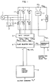
- Fig. 1 is a circuit diagram showing a first embodiment of the present invention.
- the circuit arrangement includes an AC power source 1, input end capacitors 2, a gate circuit 3, a pulse selecting circuit 4, a pulse width modulation (hereinafter abbreviated to PWM) control circuit 5, a comparator circuit 6, a DC potential transformer (hereinafter abbreviated to DCPT) 7, a load 8, and gate turn-off silicon controlled rectifiers (hereinafter abbreviated to GTOs) 11-16 which are a kind of self-extinction elements.
- the GTOs 11-16 constitute a converter unit in the form of a bridge circuit and the AC power source 1 is connected to the input side of the converter unit.
- the input end capacitors 2 are connected to the way between the AC power source 1 and the converter unit.
- the load 8 is connected to the output side of the converter unit through a DC reactor DCL.
- the DCPT 7 detects a voltage e' DCL across the DC reactor DCL to produce an output signal EDCL .
- the comparator circuit 6 compares the output signal e DCL with a predetermined overvoltage setting value e ov so as to produce an output signal P ov only when the signal e DCL is larger than the overvoltage setting value e ov , the signal P ov being applied to the pulse selecting circuit 4.
- the converter unit constituted by the bridge circuit of the GTOs 11-16 is controlled by the PWM control circuit 5, the pulse selecting circuit 4, and the gate circuit 3.
- Fig. 2 is a circuit diagram showing a specific arrangement of the pulse selecting circuit 4 shown in Fig. 1.
- the pulse selecting circuit 4 is constituted by six OR circuits 41-46. Ths output signal P ov is applied to one input of each of the OR circuits 41-46, and gate signal patterns P u -P z are applied from the PWM control circuit 5 to the respective other inputs of the OR circuits 41-46.
- the OR circuits 41-46 respectively produce output signals P GU- P GZ which are applied to the gate circuit 3.
- Fig. 3 is a time chart for explaining the operation of the PWM control circuit 5 and the pulse selecting circuit 4 shown in Fig. 1.
- V u , V v , and V w represent respective phase voltages of the AC power source 1
- e c and e m represent respectively a carrier wave and a modulating wave for forming a PWM basic pattern PTN.
- PTN represents an inverted signal of the PWM basic pattern PTN.
- An unequal-period triangular wave e' m is synchronized with the rising and falling of the PWM basic pattern PTN and is compared, as shown in the drawing, with a DC voltage command value e d * applied to the PWM control circuit 5, so as to obtain a shoot-through pulse S.
- D l -D 6 represent distribution signals and P F and P, represent PWM patterns having a period of 60 degrees for actually forming gate signals.
- the PWM patterns P, and P R and the shoot-through pulse S are distributed to the respective phases in accordance with the distribution signals D l -D 6 to thereby obtain the gate signal patterns P u -P z which are applied to the pulse selecting circuit 4 as shown in Figs. 1 and 2.
- the gate signal patterns P u -P z are ORed with the output signal P ov of the comparator circuit 6 through the OR circuits 41-46 to thereby form the gate circuit input signals P GU ⁇ P Gz .
- Such a technique to form the gate signal patterns P u- P z as described above is well known conventionally.
- the inductance value of the DC reactor used in the current-type converter is large, for example, several tens mH, so zhat the voltage e' DCL generated across the DC reactor in accordance with the above equation is very large.
- the output signal e DCL of the DCPT 7 proportional to the DC reactor terminal voltage e' DCL is compared with the overvoltage setting value e ov in the comparator circuit 6, so that the output signal P ov of the comparator circuit 6 is made high ("H") when e DCL ⁇ e ov while made low (“L”) when e DCL ⁇ e ov.
- the terminal voltage of the DC reactor DCL is detected by means of the DCPT 7 and compared with the overvoltage setting value in the comparator circuit 6 so as to make it possible to select pulses in the pulse selecting circuit 4, so that in case of occurrence of an overvoltage, the overvoltage can be suppressed by applying a turn-on signal to all the self-extinction elements GTOs 11-16 to thereby shoot-through the DC circuit. Accordingly, it is possible to protect the converter by means of a very simple arrangement and to carry out continuous operation of the converter.
- Fig. 4 shows a second embodiment of the present invention and in Fig. 4 the same parts as those in Fig. 1 are correspondingly referenced.
- the second embodiment is featured in that in addition to the gate signal patterns P u -P z from the PWM control circuit 5 and the output signal P ov from the comparator circuit 6, auxiliary signals P' u -P' z obtained from the PWM control circuit 5 are applied to the pulse selecting circuit 4.
- Fig. 5 shows a specific example of the pulse selecting circuit 4 shown in Fig. 4.
- the pulse selecting circuit 4 is constituted by OR circuits 41-46 and AND circuits 47-58.
- the gate signal patterns P u -P z are selected so as to be the input signals P GU -P GZ to the gate circuit 3 when the output P ov of the comparator circuit 6 is "L”, while the auxiliary signals P' u -P' z are selected so as to be the input signals PGU-PGZ to the gate circuit 3 when the output P ov of the comparator circuit 6 is "H".
- Fig. 6 is a time chart for explaining an operation of the second embodiment of Fig. 4.
- the process to the production of the gate signal patterns P u -P z is the same as that in the foregoing first embodiment.
- the auxiliary signals P' u ⁇ P' z are produced in the following manner.
- the auxiliary signal P' u is set to be a signal which is "H" in the period where the instantaneous voltage Vu ofthe U phase of the AC power source is higher than the instantaneous voltages of any other phases, and similarly to this, the auxiliary signals P' v and P' w are set respectively corresponding to the instantaneous voltages v v and v w .
- the auxiliary signal P' x is set to be a signal which is "H" in the period where the instantaneous voltage Vu of the U phase of the AC power source is lower than the instantaneous voltages of any other phases, and similarly to this, the auxiliary signals P'y and P' z are set respectively corresponding to the instantaneous voltages v v and v w .
- auxiliary signals P' u- P' z act to turn on the self-extinction element of the phase having the highest instantaneous source voltage among those self-extinction elements of the positive polarity arms of the bridge circuit of the converter unit, while act to turn on the self-extinction element of the phase having the lowest instantaneous source voltage among those self-extinction elements of the negative polarity arms of the bridge circuit of the same converter unit.
- the gate circuit input signals P GU ⁇ P GZ are switched over to the auxiliary signals P' u -P' z by the pulse selecting circuit 4 so that the respective self-extinction elements of the phases having the highest and lowest instantaneous phase voltages are turned off at this point in time. Accordingly, a closed circuit from the AC power source 1 to the same through the self-extinction elements in the on-state, the DC reactor DCL, and the load 8 so as to increase the current flowing into the load 8 is formed so that an overvoltage generated at the DC reactor DCL can be suppressed.
- the second embodiment is suitable to a converter employing self-extinction elements having a small withstand voltage in comparison with the current capacity thereof because the two self-extinction elements having the largest potential difference therebetween are turned on so that the overvoltage can be suppressed while the load current is increased.
- the auxiliary pulse signals are selected by means of the pulse selecting circuit 4 so as to suppress an overvoltage at the DC reactor DCL so that it is possible to achieve proper protection of the converter in accordance with the instantaneous values of the source phase voltage and it is possible to carry out continuous operation of the converter.
- the auxiliary signals P' u -P' z are arranged such that a turn-on signal is applied to the self-extinction element having the highest instantaneous source voltage among the self-extinction elements in the positive polarity arms of the converter unit and to the self-extinction element having the lowest instantaneous source voltage among the self-extinction elements in the negative polarity arms of the converter unit in the foregoing second embodiment
- the auxiliary signals may be arranged such that a turn-on signal is applied to the self-extinction element having the lowest instantaneous source voltage among the self-extinction elements in the positive polarity arms and to the self-extinction element having the highest instantaneous source voltage among the self-extinction elements in the negative polarity arms.
- the operation in this modification is shown in the time chart of Fig.
- this modification is suitable to a current-type converter which employs a self-extinction elements having a small current capacity in comparison with the withstand voltage thereof.
- Fig. 8 is a time chart showing the operation of another modification of the second embodiment illustrated in Figs. 4 and 5, in which auxiliary signals P' u- P' z different in form from those used in the second embodiment are employed.
- the auxiliary signals P' u -P' z can be formed in the following manner. That is, the PWM basic pattern PTN is distributed in accordance with the distribution signals D 1 ⁇ D 8 to thereby obtain the auxiliary signals P' u- P' z . In this case, the shoot-through pulse is not distributed. In the period I, for example, the signals P' u and P' w have respective patterns logically inverted from each other.
- the gate circuit input signals P GU -P GZ are switched over to the auxiliary signals P' u -P' z by the pulse selecting circuit 4 so that the converter is operated with the patterns P' u -P' z in the state where the width of the shoot-through pulse is zero. Accordingly, a current flows from the AC power source 1 into the load 8 through the turned-on self-extinction elements in the two arms so that an overvoltage at the DC reactor can be suppressed.
- the auxiliary signals P' u -P' z are selected by the pulse selecting circuit 4 so that an overvoltage at the DC reactor can be suppressed.
- the PWM control is also carried out so that the protection and continuous operation of the converter can be carried out without disturbing the power source current waveform.
- Fig. 9 shows a circuit arrangement of a third embodiment of the present invention.
- the self-extinction elements GTOs 11-16 are employed as elements constituting the main circuit of the converter in the first and second embodiments
- switching elements SW u -SW z having the following characteristics are employed as the constituent elements 11'-16' of the main circuit in this third embodiment.
- Zener breakdown is caused in the elements owing to the foregoing characteristic (2) so as to make the elements conductive to form a closed current circuit including the DC reactor so that the overvoltage generated at the DC reactor can be suppressed.
- Such a switching element having the foregoing characteristics (1) and (2) may be constituted by a GTO and varisters or Zener diodes connected to the GTO in parallel thereto in the forward and backward directions as shown by a reference numeral 13' representatively.
- the elements can be protected without providing any protecting device for the suppression of an overvoltage, so that the main circuit and the control circuit can be made extremely simple in arrangement. Further, an overvoltage has been suppressed, the elements return to their normal operating state from Zener breakdown so that the converter can be continuously operated.
- the overvoltage is detected by means of the DCPT and the gate signals are controlled by the pulse selecting circuit, so that the converter can be protected from the overvoltage and the operation of the converter can be continuously carried out when the overvoltage has been suppressed.
Landscapes
- Engineering & Computer Science (AREA)
- Power Engineering (AREA)
- Rectifiers (AREA)
- Dc-Dc Converters (AREA)
- Inverter Devices (AREA)
Description
- The present invention relates to a current-type converter with overvoltage protection and particularly to an apparatus suitable for protecting a current-type converter from occurrence of an overvoltage due to employment of self-extinction elements in the converter.
- Generally, as a system for converting AC power into DC one, there have been used voltage-type converters and current-type converters.
- Recently, various trials have been carried out for improving a power factor or the like by using self-extinction elements in such converters. For example, a voltage-type converter employing self-extinction elements have been proposed in US 4,361,866, etc.
- On the other hand, various current-type converters employing self-extinction elements have been proposed. In such current-type converters, however, there is a problem that an overvoltage is caused when a current is cut off. Protection of a current-type converter from such an overvoltage is discussed in a paper by Yoshioka et al, "PWM GTO Converter of New Commutation Energy System" (The Institute of Electrical Engineers of Japan, Semiconductor Power Conversion Society, Material SPC-84-60). In this paper, no sufficient consideration has been made onto a point how to protect main circuit elements of the current-type converter from an overvoltage caused across a DC reactor provided at the output side of the converter, when an erroneous turn-off pulse is mixed at any point in time into a gate signal due to noises or the like. This is because the protecting apparatus disclosed in the above paper is for overvoltage suppression and energy feeding back in commutation of the main circuit current and cannot cope with an overvoltage caused in any point in time, so that the period in which an overvoltage can be suppressed is limited to the time of commutation. Further, in the conventional converter protecting apparatus, there has been another problem that the arrangement of the protecting apparatus is complicated because a diode bridge, capacitors, self-extinction elements are used.
- GB-A-2 116 786 discloses a current-type AC-DC converter in accordance with the first part of
claim 1. The known circuit is designed to suppress overvoltages which may occur due to a time lag between the application of the turn-on signal to the self-extinction elements and the start of the DC current flow. To this end, a current path is established by applying the turn-on signal previously, thereby preventing the occurrence of an overvoltage. - It is an object of the present invention to protect a current-type AC-DC converter comprising self-extinction elements against overvoltages caused by erroneous gate pulses.
- To meet this object, the invention provides an AC-DC converter as characterized in
claim 1. Accordingly, an overvoltage due to the DC reactor is detected and the self-extinction elements are accordingly controlled to form a closed circuit including the DC reactor, thereby suppressing the overvoltage. The converter remains operable continuously after such overvoltage occurrence. - Above and other objects and features of the present invention will become more apparent when read the following description about preferred embodiments of the invention in conjunction with the accompanying drawings.
-
- Fig. 1 is a circuit diagram showing a first embodiment of the current-type converter according to the present invention;
- Fig. 2 is a circuit diagram showing the pulse selecting circuit in the first embodiment of Fig. 1;
- Fig. 3 is a time chart for explaining the operation of the first embodiment of Fig. 1;
- Fig. 4 is a circuit diagram showing a second embodiment of the current-type converter according to the present invention;
- Fig. 5 is a circuit diagram showing the pulse selecting circuit in the second embodiment of Fig. 4;
- Fig. 6 is a time chart for explaining an example of the operation of the embodiment of Fig. 4;
- Fig. 7 is a time chart for explaining another example of the operation of the embodiment of Fig. 4;
- Fig. 8 is a time chart for explaining a further example of the operation of the embodiment of Fig. 4; and
- Fig. 9 is a circuit diagram showing a third embodiment of the current-type converter according to the present invention.
- Referring to the drawings, the invention will be described more in detail hereunder with respect to various embodiments thereof.
- Fig. 1 is a circuit diagram showing a first embodiment of the present invention. In Fig. 1, the circuit arrangement includes an
AC power source 1,input end capacitors 2, agate circuit 3, apulse selecting circuit 4, a pulse width modulation (hereinafter abbreviated to PWM)control circuit 5, acomparator circuit 6, a DC potential transformer (hereinafter abbreviated to DCPT) 7, aload 8, and gate turn-off silicon controlled rectifiers (hereinafter abbreviated to GTOs) 11-16 which are a kind of self-extinction elements. As shown in the drawing, the GTOs 11-16 constitute a converter unit in the form of a bridge circuit and theAC power source 1 is connected to the input side of the converter unit. Theinput end capacitors 2 are connected to the way between theAC power source 1 and the converter unit. Theload 8 is connected to the output side of the converter unit through a DC reactor DCL. Under the condition, the DCPT 7 detects a voltage e'DCL across the DC reactor DCL to produce an output signal EDCL. Thecomparator circuit 6 compares the output signal eDCL with a predetermined overvoltage setting value eov so as to produce an output signal Pov only when the signal eDCL is larger than the overvoltage setting value eov, the signal Pov being applied to thepulse selecting circuit 4. The converter unit constituted by the bridge circuit of the GTOs 11-16 is controlled by thePWM control circuit 5, thepulse selecting circuit 4, and thegate circuit 3. - Fig. 2 is a circuit diagram showing a specific arrangement of the
pulse selecting circuit 4 shown in Fig. 1. As shown in the drawing, thepulse selecting circuit 4 is constituted by six OR circuits 41-46. Ths output signal Pov is applied to one input of each of the OR circuits 41-46, and gate signal patterns Pu-Pz are applied from thePWM control circuit 5 to the respective other inputs of the OR circuits 41-46. The OR circuits 41-46 respectively produce output signals PGU-PGZ which are applied to thegate circuit 3. - Fig. 3 is a time chart for explaining the operation of the
PWM control circuit 5 and thepulse selecting circuit 4 shown in Fig. 1. In Fig. 3, Vu, Vv, and Vw represent respective phase voltages of theAC power source 1, and ec and em represent respectively a carrier wave and a modulating wave for forming a PWM basic pattern PTN. PTN represents an inverted signal of the PWM basic pattern PTN. An unequal-period triangular wave e'm is synchronized with the rising and falling of the PWM basic pattern PTN and is compared, as shown in the drawing, with a DC voltage command value ed * applied to thePWM control circuit 5, so as to obtain a shoot-through pulse S. Dl-D6 represent distribution signals and PF and P, represent PWM patterns having a period of 60 degrees for actually forming gate signals. The PWM patterns P, and PR and the shoot-through pulse S are distributed to the respective phases in accordance with the distribution signals Dl-D6 to thereby obtain the gate signal patterns Pu-Pz which are applied to thepulse selecting circuit 4 as shown in Figs. 1 and 2. In thepulse selecting circuit 4 shown in Fig. 2, the gate signal patterns Pu-Pz are ORed with the output signal Pov of thecomparator circuit 6 through the OR circuits 41-46 to thereby form the gate circuit input signals PGU―PGz. Such a technique to form the gate signal patterns Pu-Pz as described above is well known conventionally. - Assume now that, for example, an erroneous turn-off pulse is mixed into the gate signal pattern Pu to thereby turn the
GTO 11 off at the point intime ① in Fig. 3. At the point intime ①, therefore, only the GTO 15 is in the on-state among all the GTOs constituting the converter unit. Accordingly, the circuit including theload 8 is opened and the voltage e'DCL as shown in the following equation is generated across the DC reactor DCL due to the energy which has been stored in the DC reactor DCL.
- Generally, the inductance value of the DC reactor used in the current-type converter is large, for example, several tens mH, so zhat the voltage e'DCL generated across the DC reactor in accordance with the above equation is very large. The output signal eDCL of the DCPT 7 proportional to the DC reactor terminal voltage e'DCL is compared with the overvoltage setting value eov in the
comparator circuit 6, so that the output signal Pov of thecomparator circuit 6 is made high ("H") when eDCL≧eov while made low ("L") when eDCL<eov. When the output signal Pov is "H", all the respective outputs of the OR circuits 41-46, that is, all the gate circuit input signals PGU―PGz become "H". Accordingly, all the GTOs 11-16 are fed with on-gate signals so that the DC circuit becomes a shoot-through state to thereby suppress the overvoltage which has been so far generated across the DC reactor. - As described above, in the first embodiment illustrated in Fig. 1, the terminal voltage of the DC reactor DCL is detected by means of the DCPT 7 and compared with the overvoltage setting value in the
comparator circuit 6 so as to make it possible to select pulses in thepulse selecting circuit 4, so that in case of occurrence of an overvoltage, the overvoltage can be suppressed by applying a turn-on signal to all the self-extinction elements GTOs 11-16 to thereby shoot-through the DC circuit. Accordingly, it is possible to protect the converter by means of a very simple arrangement and to carry out continuous operation of the converter. - Fig. 4 shows a second embodiment of the present invention and in Fig. 4 the same parts as those in Fig. 1 are correspondingly referenced. The second embodiment is featured in that in addition to the gate signal patterns Pu-Pz from the
PWM control circuit 5 and the output signal Pov from thecomparator circuit 6, auxiliary signals P'u-P'z obtained from thePWM control circuit 5 are applied to thepulse selecting circuit 4. Fig. 5 shows a specific example of thepulse selecting circuit 4 shown in Fig. 4. In Fig. 5, thepulse selecting circuit 4 is constituted by OR circuits 41-46 and AND circuits 47-58. In thepulse selecting circuit 4 shown in Fig. 5, the gate signal patterns Pu-Pz are selected so as to be the input signals PGU-PGZ to thegate circuit 3 when the output Pov of thecomparator circuit 6 is "L", while the auxiliary signals P'u-P'z are selected so as to be the input signals PGU-PGZ to thegate circuit 3 when the output Pov of thecomparator circuit 6 is "H". - Fig. 6 is a time chart for explaining an operation of the second embodiment of Fig. 4. In Fig. 6, the process to the production of the gate signal patterns Pu-Pz is the same as that in the foregoing first embodiment. The auxiliary signals P'u―P'z are produced in the following manner. For example, the auxiliary signal P'u is set to be a signal which is "H" in the period where the instantaneous voltage Vu ofthe U phase of the AC power source is higher than the instantaneous voltages of any other phases, and similarly to this, the auxiliary signals P'v and P'w are set respectively corresponding to the instantaneous voltages vv and vw. On the contray, the auxiliary signal P'x is set to be a signal which is "H" in the period where the instantaneous voltage Vu of the U phase of the AC power source is lower than the instantaneous voltages of any other phases, and similarly to this, the auxiliary signals P'y and P'z are set respectively corresponding to the instantaneous voltages vv and vw. Those auxiliary signals P'u-P'z act to turn on the self-extinction element of the phase having the highest instantaneous source voltage among those self-extinction elements of the positive polarity arms of the bridge circuit of the converter unit, while act to turn on the self-extinction element of the phase having the lowest instantaneous source voltage among those self-extinction elements of the negative polarity arms of the bridge circuit of the same converter unit. When an erroneous turn-off pulse is mixed into any one of the PWM patterns Pu-Pz, the gate circuit input signals PGU―PGZ are switched over to the auxiliary signals P'u-P'z by the
pulse selecting circuit 4 so that the respective self-extinction elements of the phases having the highest and lowest instantaneous phase voltages are turned off at this point in time. Accordingly, a closed circuit from theAC power source 1 to the same through the self-extinction elements in the on-state, the DC reactor DCL, and theload 8 so as to increase the current flowing into theload 8 is formed so that an overvoltage generated at the DC reactor DCL can be suppressed. Specifically, the second embodiment is suitable to a converter employing self-extinction elements having a small withstand voltage in comparison with the current capacity thereof because the two self-extinction elements having the largest potential difference therebetween are turned on so that the overvoltage can be suppressed while the load current is increased. - As described above, according to the second embodiment of the present invention, the auxiliary pulse signals are selected by means of the
pulse selecting circuit 4 so as to suppress an overvoltage at the DC reactor DCL so that it is possible to achieve proper protection of the converter in accordance with the instantaneous values of the source phase voltage and it is possible to carry out continuous operation of the converter. - Although the auxiliary signals P'u-P'z are arranged such that a turn-on signal is applied to the self-extinction element having the highest instantaneous source voltage among the self-extinction elements in the positive polarity arms of the converter unit and to the self-extinction element having the lowest instantaneous source voltage among the self-extinction elements in the negative polarity arms of the converter unit in the foregoing second embodiment, the auxiliary signals may be arranged such that a turn-on signal is applied to the self-extinction element having the lowest instantaneous source voltage among the self-extinction elements in the positive polarity arms and to the self-extinction element having the highest instantaneous source voltage among the self-extinction elements in the negative polarity arms. The operation in this modification is shown in the time chart of Fig. 7. In this modification, a closed circuit is formed such that a decreased load current flows from the AC power source through the turned-on self-extinction elements in the converter unit so that an overvoltage at the DC reactor DCL can be suppressed. Accordingly, on the contrary to the embodiment of Fig. 6, this modification is suitable to a current-type converter which employs a self-extinction elements having a small current capacity in comparison with the withstand voltage thereof.
- Fig. 8 is a time chart showing the operation of another modification of the second embodiment illustrated in Figs. 4 and 5, in which auxiliary signals P'u-P'z different in form from those used in the second embodiment are employed. In Fig. 8, the auxiliary signals P'u-P'z can be formed in the following manner. That is, the PWM basic pattern PTN is distributed in accordance with the distribution signals D1―D8 to thereby obtain the auxiliary signals P'u-P'z. In this case, the shoot-through pulse is not distributed. In the period I, for example, the signals P'u and P'w have respective patterns logically inverted from each other. In case where an erroneous turn-off signal is mixed into any one of the gate signal patterns Pu-Pz, the gate circuit input signals PGU-PGZ are switched over to the auxiliary signals P'u-P'z by the
pulse selecting circuit 4 so that the converter is operated with the patterns P'u-P'z in the state where the width of the shoot-through pulse is zero. Accordingly, a current flows from theAC power source 1 into theload 8 through the turned-on self-extinction elements in the two arms so that an overvoltage at the DC reactor can be suppressed. - As described above according to the modification of Fig. 8, the auxiliary signals P'u-P'z are selected by the
pulse selecting circuit 4 so that an overvoltage at the DC reactor can be suppressed. At this time, the PWM control is also carried out so that the protection and continuous operation of the converter can be carried out without disturbing the power source current waveform. - Fig. 9 shows a circuit arrangement of a third embodiment of the present invention. Although the self-extinction elements GTOs 11-16 are employed as elements constituting the main circuit of the converter in the first and second embodiments, switching elements SWu-SWz having the following characteristics are employed as the constituent elements 11'-16' of the main circuit in this third embodiment.
- (1) The on/off state of each of the switching elements can be controlled by a gate signal; and
- (2) Each of the switching elements has a Zener breakdown property, the Zener voltage being changeable.
- In the case where the DC circuit of the converter is opened by an erroneous turn-off pulse to generate an overvoltage at the DC reactor so that the overvoltage is applied to the main circuit constituent elements, Zener breakdown is caused in the elements owing to the foregoing characteristic (2) so as to make the elements conductive to form a closed current circuit including the DC reactor so that the overvoltage generated at the DC reactor can be suppressed.
- Such a switching element having the foregoing characteristics (1) and (2) may be constituted by a GTO and varisters or Zener diodes connected to the GTO in parallel thereto in the forward and backward directions as shown by a reference numeral 13' representatively.
- Thus, the elements can be protected without providing any protecting device for the suppression of an overvoltage, so that the main circuit and the control circuit can be made extremely simple in arrangement. Further, an overvoltage has been suppressed, the elements return to their normal operating state from Zener breakdown so that the converter can be continuously operated.
- Thus, according to the present invention, in case of generation of an overvoltage at the DCL, the overvoltage is detected by means of the DCPT and the gate signals are controlled by the pulse selecting circuit, so that the converter can be protected from the overvoltage and the operation of the converter can be continuously carried out when the overvoltage has been suppressed.
Claims (9)
characterized in
Applications Claiming Priority (2)
| Application Number | Priority Date | Filing Date | Title |
|---|---|---|---|
| JP61020161A JPH0655032B2 (en) | 1986-02-03 | 1986-02-03 | Current type converter protection device |
| JP20161/86 | 1986-02-03 |
Publications (3)
| Publication Number | Publication Date |
|---|---|
| EP0231917A2 EP0231917A2 (en) | 1987-08-12 |
| EP0231917A3 EP0231917A3 (en) | 1988-10-05 |
| EP0231917B1 true EP0231917B1 (en) | 1990-09-12 |
Family
ID=12019432
Family Applications (1)
| Application Number | Title | Priority Date | Filing Date |
|---|---|---|---|
| EP87101368A Expired - Lifetime EP0231917B1 (en) | 1986-02-03 | 1987-02-02 | Current-type converter with overvoltage protection |
Country Status (6)
| Country | Link |
|---|---|
| US (1) | US4757436A (en) |
| EP (1) | EP0231917B1 (en) |
| JP (1) | JPH0655032B2 (en) |
| KR (1) | KR870008430A (en) |
| DE (1) | DE3764810D1 (en) |
| HK (1) | HK38391A (en) |
Families Citing this family (11)
| Publication number | Priority date | Publication date | Assignee | Title |
|---|---|---|---|---|
| JPH088778B2 (en) * | 1987-04-22 | 1996-01-29 | 株式会社日立製作所 | Current source inverter device |
| US4815052A (en) * | 1988-07-06 | 1989-03-21 | Honeywell, Inc. | Automatic overvoltage protection circuit |
| DE4229342A1 (en) * | 1992-09-04 | 1994-03-10 | Thomson Brandt Gmbh | Method and device for driving with pulsed signals |
| US5414342A (en) * | 1993-04-29 | 1995-05-09 | Unitrode Corporation | Voltage mode pulse width modulation controller |
| JPH0759256A (en) * | 1993-08-19 | 1995-03-03 | Toshiba Corp | Thyristor valve protection device |
| US6278597B1 (en) | 1999-10-05 | 2001-08-21 | International Business Machines Corporation | Conditional over-voltage protection for redundant phase-shift converters |
| KR100440345B1 (en) * | 2002-06-03 | 2004-07-15 | 주식회사 동아일렉콤 | Converter for converting a three-phase alternating current to a direct current |
| US6803748B2 (en) * | 2003-02-03 | 2004-10-12 | Delphi Technologies, Inc. | System and method for controlling load dump voltage of a synchronous machine |
| GB2508418A (en) | 2012-11-30 | 2014-06-04 | Control Tech Ltd | Thyristor rectifier charge rate controller |
| US11196338B2 (en) * | 2017-12-29 | 2021-12-07 | North Carolina State University | Semiconductor topologies and devices for soft starting and active fault protection of power converters |
| CN108307117B (en) * | 2018-02-09 | 2020-03-10 | 湖南大学 | Full-field optical measurement multifunctional synchronous control device and method |
Family Cites Families (7)
| Publication number | Priority date | Publication date | Assignee | Title |
|---|---|---|---|---|
| US3622862A (en) * | 1970-10-22 | 1971-11-23 | Asea Ab | By-pass connection of static converters |
| JPS5270328A (en) * | 1975-12-10 | 1977-06-11 | Hitachi Ltd | Thyrister rectifier |
| US4044295A (en) * | 1976-12-29 | 1977-08-23 | International Business Machines Corporation | Over-voltage interrupt for a phase controlled regulator |
| US4238821A (en) * | 1979-04-24 | 1980-12-09 | General Electric Company | Method and apparatus for a variable frequency inverter system having commutation fault detection and correction capabilities |
| JPS5683268A (en) * | 1979-12-10 | 1981-07-07 | Hitachi Ltd | Controlling method for inverter |
| JPS58154377A (en) * | 1982-03-10 | 1983-09-13 | Hitachi Ltd | Power converter |
| JPS60156270A (en) * | 1984-01-25 | 1985-08-16 | Hitachi Ltd | Drive controller of power converter |
-
1986
- 1986-02-03 JP JP61020161A patent/JPH0655032B2/en not_active Expired - Lifetime
-
1987
- 1987-02-02 US US07/009,478 patent/US4757436A/en not_active Expired - Fee Related
- 1987-02-02 DE DE8787101368T patent/DE3764810D1/en not_active Expired - Lifetime
- 1987-02-02 EP EP87101368A patent/EP0231917B1/en not_active Expired - Lifetime
- 1987-02-03 KR KR870000833A patent/KR870008430A/en not_active Withdrawn
-
1991
- 1991-05-16 HK HK383/91A patent/HK38391A/en unknown
Also Published As
| Publication number | Publication date |
|---|---|
| US4757436A (en) | 1988-07-12 |
| EP0231917A2 (en) | 1987-08-12 |
| EP0231917A3 (en) | 1988-10-05 |
| JPH0655032B2 (en) | 1994-07-20 |
| HK38391A (en) | 1991-05-24 |
| JPS62181679A (en) | 1987-08-10 |
| DE3764810D1 (en) | 1990-10-18 |
| KR870008430A (en) | 1987-09-26 |
Similar Documents
| Publication | Publication Date | Title |
|---|---|---|
| KR910008547B1 (en) | Power converter of current type | |
| US4354223A (en) | Step-up/step down chopper | |
| US6339316B1 (en) | Exciter for generator | |
| SE504522C2 (en) | Power transmission with high voltage direct current comprising more than two inverter stations | |
| EP0868014A1 (en) | A high voltage converter circuit | |
| US4757436A (en) | Current-type converter protecting apparatus | |
| JP3715807B2 (en) | Power phase adjusting device and power transmission system using the power phase adjusting device | |
| US4736286A (en) | Switching power supply | |
| US5535085A (en) | Snubber energy recovery circuit for protecting switching devices from voltage and current | |
| US6437998B1 (en) | Rectifying circuit and control method therefor | |
| EP0079130A1 (en) | Reactive snubber for inductive load clamp diodes | |
| US6160726A (en) | Power converter including positive bus ground | |
| EP0309919B1 (en) | A power conversion apparatus | |
| JPH0823779B2 (en) | Power control device | |
| EP0129909B1 (en) | Method and apparatus for controlling reverse-conducting gto thyristor | |
| WO1994014230A1 (en) | Series resonant converter having a three part resonant inductor | |
| US4486824A (en) | PWM Converter with control circuit responsive to minimum holding current | |
| GB2051507A (en) | Selective commutation circuit for an inverter | |
| JPH0821861A (en) | Power converter failure detection circuit | |
| GB1583891A (en) | Power supply circuit | |
| JP4217897B2 (en) | PWM cycloconverter and input voltage detection method thereof | |
| US20030103305A1 (en) | Method and circuit for the protection of a thyristor | |
| Liptak et al. | Regenerative Controller for a VoItage-Source Inverter Drive | |
| JPH04275071A (en) | Gto inverter | |
| CA1179015A (en) | Twin transformer inverter |
Legal Events
| Date | Code | Title | Description |
|---|---|---|---|
| PUAI | Public reference made under article 153(3) epc to a published international application that has entered the european phase |
Free format text: ORIGINAL CODE: 0009012 |
|
| AK | Designated contracting states |
Kind code of ref document: A2 Designated state(s): CH DE FR GB IT LI NL SE |
|
| PUAL | Search report despatched |
Free format text: ORIGINAL CODE: 0009013 |
|
| AK | Designated contracting states |
Kind code of ref document: A3 Designated state(s): CH DE FR GB IT LI NL SE |
|
| RHK1 | Main classification (correction) |
Ipc: H02M 7/162 |
|
| 17P | Request for examination filed |
Effective date: 19881028 |
|
| 17Q | First examination report despatched |
Effective date: 19890207 |
|
| GRAA | (expected) grant |
Free format text: ORIGINAL CODE: 0009210 |
|
| AK | Designated contracting states |
Kind code of ref document: B1 Designated state(s): CH DE FR GB IT LI NL SE |
|
| PG25 | Lapsed in a contracting state [announced via postgrant information from national office to epo] |
Ref country code: IT Free format text: LAPSE BECAUSE OF FAILURE TO SUBMIT A TRANSLATION OF THE DESCRIPTION OR TO PAY THE FEE WITHIN THE PRE;WARNING: LAPSES OF ITALIAN PATENTS WITH EFFECTIVE DATE BEFORE 2007 MAY HAVE OCCURRED AT ANY TIME BEFORE 2007. THE CORRECT EFFECTIVE DATE MAY BE DIFFERENT FROM THE ONE RECORDED.SCRIBED TIME-LIMIT Effective date: 19900912 Ref country code: NL Effective date: 19900912 |
|
| REF | Corresponds to: |
Ref document number: 3764810 Country of ref document: DE Date of ref document: 19901018 |
|
| ET | Fr: translation filed | ||
| NLV1 | Nl: lapsed or annulled due to failure to fulfill the requirements of art. 29p and 29m of the patents act | ||
| PLBE | No opposition filed within time limit |
Free format text: ORIGINAL CODE: 0009261 |
|
| STAA | Information on the status of an ep patent application or granted ep patent |
Free format text: STATUS: NO OPPOSITION FILED WITHIN TIME LIMIT |
|
| 26N | No opposition filed | ||
| PGFP | Annual fee paid to national office [announced via postgrant information from national office to epo] |
Ref country code: FR Payment date: 19911218 Year of fee payment: 6 |
|
| PGFP | Annual fee paid to national office [announced via postgrant information from national office to epo] |
Ref country code: SE Payment date: 19920108 Year of fee payment: 6 |
|
| PGFP | Annual fee paid to national office [announced via postgrant information from national office to epo] |
Ref country code: GB Payment date: 19920123 Year of fee payment: 6 |
|
| PGFP | Annual fee paid to national office [announced via postgrant information from national office to epo] |
Ref country code: DE Payment date: 19920427 Year of fee payment: 6 |
|
| PGFP | Annual fee paid to national office [announced via postgrant information from national office to epo] |
Ref country code: CH Payment date: 19920429 Year of fee payment: 6 |
|
| PG25 | Lapsed in a contracting state [announced via postgrant information from national office to epo] |
Ref country code: GB Effective date: 19930202 |
|
| PG25 | Lapsed in a contracting state [announced via postgrant information from national office to epo] |
Ref country code: SE Effective date: 19930203 |
|
| PG25 | Lapsed in a contracting state [announced via postgrant information from national office to epo] |
Ref country code: LI Effective date: 19930228 Ref country code: CH Effective date: 19930228 |
|
| GBPC | Gb: european patent ceased through non-payment of renewal fee |
Effective date: 19930202 |
|
| PG25 | Lapsed in a contracting state [announced via postgrant information from national office to epo] |
Ref country code: FR Effective date: 19931029 |
|
| REG | Reference to a national code |
Ref country code: CH Ref legal event code: PL |
|
| PG25 | Lapsed in a contracting state [announced via postgrant information from national office to epo] |
Ref country code: DE Effective date: 19931103 |
|
| REG | Reference to a national code |
Ref country code: FR Ref legal event code: ST |
|
| EUG | Se: european patent has lapsed |
Ref document number: 87101368.6 Effective date: 19930912 |