EP0230838A2 - Pulse width modulator and demodulator - Google Patents
Pulse width modulator and demodulator Download PDFInfo
- Publication number
- EP0230838A2 EP0230838A2 EP86402963A EP86402963A EP0230838A2 EP 0230838 A2 EP0230838 A2 EP 0230838A2 EP 86402963 A EP86402963 A EP 86402963A EP 86402963 A EP86402963 A EP 86402963A EP 0230838 A2 EP0230838 A2 EP 0230838A2
- Authority
- EP
- European Patent Office
- Prior art keywords
- duration
- pulses
- pulse
- modulated
- sampling period
- Prior art date
- Legal status (The legal status is an assumption and is not a legal conclusion. Google has not performed a legal analysis and makes no representation as to the accuracy of the status listed.)
- Withdrawn
Links
Images

Classifications
-
- H—ELECTRICITY
- H03—ELECTRONIC CIRCUITRY
- H03M—CODING; DECODING; CODE CONVERSION IN GENERAL
- H03M1/00—Analogue/digital conversion; Digital/analogue conversion
- H03M1/12—Analogue/digital converters
- H03M1/14—Conversion in steps with each step involving the same or a different conversion means and delivering more than one bit
- H03M1/145—Conversion in steps with each step involving the same or a different conversion means and delivering more than one bit the steps being performed sequentially in series-connected stages
- H03M1/146—Conversion in steps with each step involving the same or a different conversion means and delivering more than one bit the steps being performed sequentially in series-connected stages all stages being simultaneous converters
Definitions
- the present invention relates to a modulator at one end of a transmission link for modulating pulses in duration as a function of an incoming analog or digital signal, as well as to a demodulator at another end of the link for demodulating the pulses modulated in duration transmitted by the modulator in samples of the incoming signal which are then smoothed to restore the incoming signal.
- the main object of the invention is to provide such modulator and demodulator which are completely asynchronous, that is to say having completely independent time bases.
- a sampling period of the incoming signal and a carrier frequency of the pulses are fixed by respective independent time bases so that in the demodulator, different clock signals necessary for operation of the demodulator are established, not by means of any rhythm recovery from the pulses received, but from a locally produced base clock frequency.
- each of the time-multiplexed channels is characterized by a sampling period possibly different from those of the other channels and a carrier frequency different from those of the other channels.
- the carrier frequencies may be different from a few hertz, taking into account the performance of pulse detection devices as a function of their duration or of carriers as a function of their frequency included in the demodulator, and thus do not cause a significant widening of the bandwidth of the transmission means currently used for MIO signals.
- a modulator is as defined in claim 1.
- the quantization words represent quantized values of samples according to a quantization law with IJ quantified values, and each quantization word is composed of a first part comprising I bits among which only one bit has a predetermined logic state and has a rank in said first part indicating a first quantized value of the sample among I quantized values, and of a second part comprising J bits among which only one bit has the predetermined state and has a rank in said second part indicating a second quantized value of the sample among J quantized values in the vicinity of said first quantized value of the sample; the sampling means produce a pulse having a position in each sampling period which is a linear function of the rank of said bit in the first part of the sampled word and of the rank of said bit in the second part of the sampled word.
- the input means are a quantization circuit continuously quantizing the instantaneous voltage of the incoming signal.
- This quantification circuit is of the type described in French patent application 86-00305 filed on January 10, 1986.
- the input means are transcoding means converting each byte of the MIC signal into a quantization word at each sampling period.
- a demodulator is as defined in claim 11.
- the means for loading and delivering comprise counting means receiving asynchronous clock pulses of any clock pulses in the modulator, triggered by the detected leading edge of each first pulse modulated in position and reset to zero after a sampling period following the detection of the leading edge, to establish the first and second durations.
- the first and second pulses modulated in position and additional by pair in a sampling period are transmitted by the modulator.
- the first pulses modulated in position have widths less than a first duration less than the sampling period and the modulator comprises means for producing a second pulse modulated in duration having a duration complementary to the duration of the first pulse in the first duration of each sampling period; the demodulator then comprises means for verifying the complementarity of the durations of first and second pulses in the first duration in order to deliver one of the first and second pulses to the means for detecting the rising edge and to the means for loading and delivering when the complementarity is checked.
- the demodulator can include means for inhibiting the delivery of one of the first and second pulses modulated in position during a sampling period to the means for detecting the rising edge and to the means for charging and delivering when the complementarity of the durations of first and second pulses received is not verified, and means for delivering one of first and second modulated pulses in position during a sampling period to the means for detecting the rising edge and to the means for loading and delivering when the other of the first and second pulses is not received or when a carrier frequency modulated by the other of the first and second pulses in the modulator is not detected in the demodulator.
- the modulator and demodulator assembly according to the invention offers an anti-parasitic and anti-fading action which, added to the advantage of a very narrow bandwidth, gives the assembly very high quality and transmission security, especially in radio broadcasts.
- a pulse modulator in duration MOD which according to a first embodiment, is intended to quantify and sample an incoming modulating analog analog signal SE and to convert words representing quantized values of the signal into durations impulse.
- the incoming modulating signal is, in general, an analog signal which can be an amplitude, frequency or phase modulation signal, such as for example a low frequency signal of the telephone signal type.
- the modulator MOD comprises a quantization circuit 1 for instantaneously quantifying the incoming voltage signal in IJ quantization intervals, a sampling circuit 2 for taking during a sampling period T e a quantization word transmitted by the circuit 2 and representative of a quantized value of the incoming signal, a modulation circuit 3 for converting each quantized value into a pulse duration modulating a carrier, and a time base 4 controlling circuits 2 and 3.
- a DEM demodulator receiving pulses of different durations transmitted by the modulation circuit 3 through an MV transmission means, for example such as a telephone line in a switched telephone network.
- the demodulator DEM includes a detection and validation circuit 5 for removing the carrier, detecting the pulses received and, preferably, for validating their duration, a demodulation circuit 6 for converting each detected pulse into a duration-dependent voltage sample of the detected pulse, and a time base 7.
- the quantization circuit 1 is an acyclic quantization circuit with high operating speed such as that described in French patent application 86-00305 filed on January 10, 1986 in the name of the current applicant. .
- Circuit 1 is divided into two quantizers QUA and qua by a differential input transformer TD.
- the incoming signal SE to be quantified is applied to a double primary winding EP + ep of the transformer TD and is reproduced and positively biased at the terminals of two secondary half-windings ES and es of the transformer.
- Each of the secondary half-windings ES, es has a terminal carried through a potentiometer PT, pt to a suitable positive voltage VMOY corresponding to an average value of the peak-to-peak amplitude of the incoming signal.
- the other terminals of the half-windings ES and es constitute input terminals BE, be of the quantizers QUA and qua respectively.
- Each of the cells C i of rows i between 1 and I-2 contains a detection circuit CD i for detecting an incoming voltage greater than a decision level defined by a lower limit voltage VT i and included in the respective quantization interval VT i to VT i + 1 , and a signaling circuit CS i for signaling by a logic state "1" to an output terminal BS i of the cell an incoming voltage included in this quantization interval.
- the first cell C0 only comprises a signaling circuit CS0 constituted by a simple inverter IN0, and the last cell C I-1 contains a detection circuit CD I-1 similar to those CD1 to CD I-2 in cells C1 to C I-2 , and a signaling circuit CS I-1 comprising only one diode D3 I-1 .
- the terminals of the resistors R21 and R2 I-1 are thus brought to the voltage limits VT0 to VT I quantization intervals.
- a terminal T i of the resistor R2 i connected to the resistor R2 i + 1 in the cell of rank i + 1 is brought to the voltage VT i , which is transferred through a diode D2 i to a terminal S i of a network of resistors and diodes in series.
- This latter network comprises between the input terminal BE and the anode of the diode D2 I-1 in the cell C I-1 , sets of diode and resistance in series D11, R11 to D1 I-1 , R1 I- 1 ; in a cell C i , the resistor R1 i is connected between emitters and base of a bipolar PNP transistor TR i .
- the diodes D11 to D1 i are conducting and the transistors TR1 to TR i are activated, or in other words, the transistor TR i is activated for a voltage at terminal BE exceeding the lower limit voltage VT i of the interval (VT i , VT i + 1 ) associated with cell C i , thanks to the voltage division created by the network of resistors R21 to R2 I-1 and the diode and resistance network R11 to R12 I-1 and D11 to D1 I-1 .
- the voltage at the BE terminal is adjusted to an average voltage substantially equal to VMOY and included in the quantization interval (VT I / 2-1 , VT I / 2 ) in particular when the quantification is uniform.
- the ohmic values of the resistances can be chosen to achieve a uniform quantization, or a non-uniform quantization deduced for example from a known logarithmic function of the curve type. compression of quantization levels for pulse code modulation of the MIC type.
- an AND gate P i has a first input connected to the collector of the transistor TR i in order to set to "1" an output terminal BS i of the cell C i only when the incoming voltage at the terminal BE is between VT i and VT i + 1 .
- the transistor TR i is blocked, which closes the gate P i .
- the output terminal of one of the cells C i + 1 to C I-1 is activated in state "1" which puts in state "0" a second input of the gate P i through a diode of the activated cell, equivalent to the diode D4 i in the cell C i , diodes in series between the activated cell and the cell C i , such as the diode D3 i in cell C i , and an inverter IN i in cell C i .
- a voltage of the polarized incoming signal between VT i and VT i + 1 is signaled by the state "1" at the output terminal BS i of the cell C i and by the state "0" at the output terminals BS0 to BS i-1 and BS i + 1 to BS I-1 of the other cells of the QUA quantizer.
- the second quantizer qua refines the quantization of the signal entering the first intervals (VT0, VT1) to (VT I-1 , VT I ) by dividing each of them into J second quantization intervals.
- the quantifier qua contains J second cells c0 to c J-1 arranged in a manner analogous to cells C0 to C I-1 .
- C0, c1 to c J-2 and c J-1 cells are respectively analogous to cells C0, C1 to C I-2 and C I-1 .
- components included in cell c j are designated by marks having lower case letters and numbers corresponding to capital letters and numbers of marks denoting equivalent components in cell C i .
- the cell numbers I and J in the quantifiers QUA and qua can be equal or different.
- the quantizer qua also includes first and second diode networks and resistors RDR1 and RDR2 for selectively applying the limit voltages of a first quantization interval when the corresponding output terminal of the first quantizer QUA is in the state "1".
- the first network RDR1 applies to the resistance r21 of the cell c1 the lower voltage of the first interval selected through a potentiometer ra1, while the second network RDR2 applies to the resistance r2 J-1 of cell c J-1 the upper limit of the first interval selected through a potentiometer ra2.
- a quantized value of the instantaneous voltage of the incoming signal is represented by a quantization word at a given instant composed of a first part having I-1 bits in the "0" state and a bit at l 'state “1" delivered in parallel by the outputs BS0 to BS I-1 and of a second part having J-1 bits in the state "0" and a bit in the state "1” delivered in parallel by the outputs bs0 to bs J-1 .
- the numbers I and J are assumed to be equal to 16 below, which corresponds to a quantization of the signal entering 256 quantization intervals.
- the sampling circuit 2 thus operates a pulse modulation in position.
- the gates PE0 to PE I-1 have first inputs connected to the output terminals BS0 to BS I-1 of the first quantizer QUA, second inputs connected to the outputs of the I stages of the counter COM, and outputs connected to I input of an OR gate, respectively.
- the gate PO has an output connected to a first input 211 of an AND gate 21 having an output connected to a clock input eh0 of the counter com.
- the gates pe0 to pe J-1 have first inputs connected to the output terminals bs0 to bs J-1 of the second quantizer qua, second inputs connected to the outputs of the J stages of the counter com, and outputs connected to J entrances of a door OR po, respectively.
- the time base 4 includes a clock 41, a preferably programmable counter 42, a D type flip-flop 43, an AND gate with two inputs 44 and a frequency divider by J 45.
- the instant ⁇ 2 determines the start of transmission of an IM1 pulse ij by the modulation circuit 3.
- the IM1 pulse ij has a duration d1 ij which is a function of the ranks i and j of the bits BS i and bs j in the state "1" in the quantization word taken and less than or equal to d M , and therefore which is proportional to the instantaneous value of the incoming signal SE.
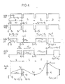
- the counter 42 and the flip-flop 43 in the time base 4 develop pulses of duration d M positioned in the periods T e as shown in a second line in FIG. 4.
- a clock input 42H of the counter 42 receives the clock signal h0 delivered by the clock 41.
- An output 421 of the counter 42 is connected to a clock input 43H of the flip-flop 43 and goes to " 1 "after a period d12 succeeding the start ⁇ 0 of a sampling period T e , as shown in the first line of FIG.
- an output 43Q of the latter then produces a pulse of duration d M from the instant ⁇ 2 of the period T e , pulse whose edge descending is obtained when an output 42M of the counter 42 sets a reset input 43R of the flip-flop 43 to "1", in response to a count of IJ clock pulses succeeding the instant ⁇ 2. Then after a count of clock pulses h0 for a period equal to d m , an output 42m of the counter 42 connected to a reset input 42R of the latter goes to "1" in order to reset the counter and outputs 421, 42M and 42m and establish a new sampling period.
- the duration d12 is equal to T e / 9, and the duration d m is equal to 0, the outputs 42M and 42m being combined, or is for example equal to T0, and is considered in the following as negligible compared to the durations d12 and d M , these being practically complementary in the period T e .
- the counter COM successively opens the doors PE0 to PE I-1 to read the I output terminals BS0 to BS I-1 of the quantizer QUA and thus detect the state "1" of one of these terminals, such as a terminal BS i , in response to the clock pulse of rank i + 1 applied to the input EH0 from time ⁇ 2.
- this pulse of rank i + 1 opens the gate 21 for a duration equal to JT0 succeeding a duration iJT0 from the instant ⁇ 2 in the sampling period T e in progress .
- a group of J consecutive clock pulses of period T0 is then applied to the clock input eh0 of the counter com by the output 213 of gate 21.
- the J clock pulses are counted in the counter com which opens successively the doors pe0 to pe N-1 to scan the J output terminals bs0 to bs J-1 of the quantizer qua and thus detect the state "1" of one of these terminals, such as a terminal bs j , in response to the clock pulse of rank j + 1 applied to the input eh0 during the duration JT0.
- the duration d12 + d1 ij - T0 determines the time position of the rising edge of the clock pulse leaving the door po in a period T e .
- the modulation circuit 3 comprises a flip-flop 30, an inverter 300, an AND gate with two inputs 31, an AND gate with three inputs 32, an inverter 33 and a generator 34 generating, preferably from the clock frequency 1 / T0, two carriers of frequency fp1 and fp2, preferably very close, by outputs 341 and 342.
- the flip-flop 30 has a setting input to "1" 30S connected to the output 421 of the counter 42, or at the input 442 of the door 42.
- a reset input to "0" 30R of the scale 30 is connected to the output 23 of the door OR po through the inverter 300.
- the rising front edge of such a pulse IM1 ij whatever i and j, is always positioned at time ⁇ 2 in a sampling period T e , as shown in a third line in Fig. 4.
- the modulation circuit 3 codes the first quantization level encountered in a pulse.
- the output 30Q of flip-flop 30 is reset to zero by the trailing edge falling from the clock pulse to terminal 23 and therefore immediately reset to zero after the pulse IM1 ij until the end of the sampling period .
- the modulation is therefore unequivocal between a pair of bits BS i and bs j in the state "1" and a pulse IM1 ij .
- the pulse IM1 ij obtained at output 30Q opens the door 31 having inputs connected to terminals 30Q and 341.
- An output 311 of the AND gate 31 transmits the pulse IM1 ij modulating the carrier frequency fp1 for the duration d1 ij .
- an output 321 of the AND gate 32 delivers a pulse IM2 ij modulating the carrier frequency fp2 and having a duration d2 ij equal to the complement of the duration d1 ij during the duration d M of the sampling period, or more generally during the duration d M + d m , i.e.
- the pulse IM2 ij always having a falling edge positioned at the end d 'a period T e , as shown in a fourth line in Fig. 4.
- the three inputs of gate 32 are respectively connected to output 421 of counter 42 in the time base, to output 30Q of flip-flop 30 through inverter 33, and to output 342 of generator 34.
- the transmission means MT conveys the frequency multiplexed IM1 ij and IM2 ij pulses in two parallel lines.
- the reception of the pairs of successive pulses IM1 ij and IM2 ij makes it possible to test the conformity of the received signal by checking that the sum of the durations of two "complementary" pulses is always constant and equal to d M , or d M + d m , during each sampling period T e .
- the modulator only comprises a quantizer QUA and a sampler ECH when the number of quantization levels is small; in this case, the output of the OR gate PO (Fig.3) is directly connected to the input 30R of the rocker 30 through the inverter 300.
- the DEM demodulator is now described with reference to Figs. 2, 5 and 6.
- pulses IM1 ij and IM2 ij modulating the carrier frequencies fp1 and fp2 are respectively received at inputs 5011 and 5012 from two carrier detectors 501 and 502 included in the circuit pulse detection and validation 5 shown in Fig. 5.
- the detectors 501 and 502 are preferably pulse detection devices according to their duration of the kind described in French patent application 85-15418 filed on October 17, 1985, in the name of the current applicant.
- detectors 501 and 502 are programmed by the time base 7 to detect alternating sinusoids of widths 1 / (2fp1) and 1 / (2fp2) and thus restore continuous voltages in response to the carriers fp1 and fp2 during the durations d1 ij and d2 ij of the pulses IM1 ij and IM2 ij respectively.
- Outputs 5021 and 5022 thus restore two pulses IM1 ij and IM2 ij without carrier, in each sampling period T e .
- the circuit 5 also includes a complementarity checking circuit 51, a complementary pulse selection circuit 52 and a control circuit 53 at the output.
- the complementarity verification circuit 51 comprises an OR-Exclusive gate 511 having two inputs respectively connected to terminals 5021 and 5022, a pulse detection device 512 connected to the output of gate 511, an AND gate 513 having a first input directly connected to output 514 of device 512 and a second input connected to output 5021 through a delay line 5211, and an inverter 515 connected to output 514 of device 512.
- an OR-Exclusive gate 511 having two inputs respectively connected to terminals 5021 and 5022, a pulse detection device 512 connected to the output of gate 511, an AND gate 513 having a first input directly connected to output 514 of device 512 and a second input connected to output 5021 through a delay line 5211, and an inverter 515 connected to output 514 of device 512.
- Device 512 is of the kind described in the aforementioned patent application 85-15418, and is programmed by the time base 7 to detect pulses of width d M , or d M + d m , at period T e , it is i.e. to detect pulses periodicals of width d M , or d M + d m , spaced by a time difference equal to d12.
- the output 514 of the device 512 is in the state "1" as long as pulses at the output of the gate 511 have widths of d M , or d M + d m , and time differences between them of d12, c ' that is, as long as pulses IM1 ij and IM2 ij are strictly complementary during the duration d M , or d M + d m , in the periods T e .
- the AND gate 513 is open to transmit the pulses IM1 ij applied by the delay line 5211 to an input 532 C of an OR gate with three inputs 531 included in the control circuit 53.
- the pulses IM2 ij are transmitted by the gate 513 by connecting the input of the delay line 5211 to the output 5022 of the detector 502, or by connecting the second input of gate 513 only to output 5022 through a delay line 5212.
- the delay line 5211 like the other delay line 5212 in the selection circuit 52, imposes a delay equal to d M or d M + d m , or equal to 2d M + T e or 2 (d M + d m ) + T e according to the type chosen of the device 512 in order to compensate for the delay imposed by the detection of pulses of duration d M , or d M + d m in the device 512.
- d M is equal to 0, or that d M can be replaced by d M + d m .
- the gate 513 is closed and an output of the inverter 515 activates an AND gate with three inputs 523 and an AND gate with two inputs 524 included in the selection circuit 52. Two conditions are then to be distinguished in the absence of pulse complementarity.
- the absence of complementarity is due to an lengthening or a shortening of the duration of one of the detected pulses IM1 ij and IM2 ij .
- the received signal is then eliminated by closing the AND gate 524 thanks to two monostable flip-flops 5251 and 5252 interconnected respectively between the terminals 5011 and 5012 and two other inputs of the AND gate 523 having an output connected to a second input of the gate 524 through an inverter 526.
- the monostable flip-flops have time constants equal to T e and are retriggerable by the rising front edges of the pulses IM1 ij and IM2 ij respectively, so that in the presence of successive and non-consecutive pulses IM1 ij and IM2 ij , door 523 is open and closes door 524 which in turn closes two AND doors with two inputs 5271 and 5272.
- the AND gates 5271 and 5272 receive by second inputs the pulses IM1 ij and IM2 ij through the delay lines 5211 and 5212 and have outputs connected to the two other inputs 5321 and 5322 of OR gate 531, respectively.
- the output of gate 523 in state "1" can command the sending back, to the transmission part comprising the modulator, of a signal requesting the repetition of part of the message, such as last character or byte transmitted.
- the complementarity is not observed by the Exclusive-OR gate 511 and the device 512, and one of the pulses IM1 ij and IM2 ij is not detected by the detectors 501 and 502.
- one of the monostable flip-flops 5251 and 5252 is not triggered which closes the door 523 and opens the door 524 which controls the passage of the detected pulse IM1 ij or IM2 ij through the respective open AND gate 5271 or 5272.
- the demodulation of the pulses IM1 ij and that of the pulses IM2 ij lead to signals in phase opposition which, in the general case and insofar as the disturbance is weak, has no effect on a phonic or digital restitution of the demodulated signal.
- the control circuit 53 comprises, in addition to the OR gate 531, two doors 533 and 534 respectively having first inputs connected to the terminal 5021 through the delay line 5211, and at the output of the OR gate 531, second connected inputs through an inverter 535 and directly to a control terminal 5C, and outputs connected to an input terminal 6E of the demodulation circuit 6 through an OR gate with two inputs 536.
- the control terminal 5C in the "1" state activates the circuits 51 and 52 of the detection and validation circuit 5 by opening the door 534 and closing the door 533 in order to transmit through the door OR 531 of the first IM1 ij pulses validated by the device 512 or of the pulses selected from among IM1 ij and IM2 ij pulses detected by the circuit 52.
- terminal 5C is at state "0"
- door 534 is closed and p orte 533 is open to transmit directly uncontrolled pulses IM1 ij without carrier delivered by the terminal 5021 through the delay line 5211.
- the demodulation circuit 6 comprises a flip-flop 61 for detecting the rising edges of the pulses IM1 ij , to which reference is made below, or possibly of the pulses IM2 ij , received at the input 6E, a circuit for reproducing samples of the incoming signal 62, and a control circuit 63 for taking samples.
- the sample reproducing circuit 62 essentially comprises a capacitor 621 which, during each sampling period, is charged by a voltage depending on the width of a pulse IM1 ij received during this period, then is completely discharged, and an element with variable resistivity in the form of a field effect transistor with high input impedance of the unijunction transistor type 622 which is supplied by the voltage memorized by the capacitor 621 and therefore proportional to the duration d1 ij of the pulse received IM1 ij and at the corresponding quantized voltage level of the incoming signal SE and established in the quantization circuit 1.
- the capacitor 621 has an armature brought to earth and another armature A which is connected to the emitter E of conductivity P of transistor 622 , to the cathode of a diode 623 through an adjustable resistor 624, and to the anode of a diode 625.
- the anode of diode 623 is connected to the input terminal 6E and to a switching terminal "1 "61S of flip-flop 61.
- Bases B1 and B2 of transistor 622 are respectively connected to earth and to an output terminal 6S of the demodulation circuit connected to an adjustable resistance terminal 626.
- the control circuit 63 comprises three AND gates with two inputs 631, 632 and 633, a counter 634 and a monostable latch triggerable by falling edge 635. First inputs of the gates 631, 632 and 633 are connected to an output 61Q of the latch bistable 61 so that these three doors are activated in response to a rising edge of a pulse IM1 ij detected at input 6E by flip-flop 61.
- Such a clock signal can be obtained from a clock supplying a clock signal of period T0 from which the time base 7 also establishes, by means of programmable frequency dividers, clock frequencies necessary for the pulse detection devices 501 , 502 and 512 in the detection and validation circuit 5.
- the time base 7 is completely independent of the time base 4 in the MOD modulator and, consequently, the modulation and demodulation operations are asynchronous and do not require a any clock recovery circuit in the DEM demodulator thanks to the 501, 502 and 512 devices.
- the counter 634 here comprises five stages and receives at a clock input 634H the clock signal of period d1 through the gate 631.
- a first output 634 M of the counter 634 is connected to a second input of the gate 632 having a output connected through the resistor 626 to the terminal 6S and therefore to the control base B2 of the transistor 622.
- a second output 6341 of the counter 634 is connected on the one hand to a second input of the gate 633 having an output connected to the cathode of diode 625 through an inverter 636, on the other hand to an input 635S of the monostable flip-flop 635 having an output 635Q connected to reset inputs 61R and 634R of flip-flop 61 and of the counter 634.
- the outputs 634 M and 6341 remain in the "0" state until the counter 634 has counted down a duration d M.
- the gate 632 is blocked and provides an earth output to block the unijunction transistor 622 and thus keep a zero voltage at terminal 6S.
- the gate 633 is blocked and its output is at "0" which blocks the diode 625 through the inverter 636 and allows charging of the capacitor 621 through the diode 623 and the resistor 624.
- the resistor 624 is adjusted beforehand so that the charge curve of the capacitor 621 for a duration equal to or less than d M is substantially a straight line. Under these conditions, the capacitor 621 is charged for the duration d1 ij of the pulse IM1 ij which is normally less than or equal to d M.
- the output 634 M of the counter goes to "1" which opens the gate 632 and turns on the transistor 622 for a duration d1 succeeding d M , the door 633 being still closed.
- this duration d1 that is to say between instants M and ⁇ M + d1 of a sampling period T e as shown in a fifth line of FIG. 4, the charge voltage of the capacitor 621 is applied to the transistor 622 and determines the conductivity of the latter so that the output terminal 6S of the demodulation circuit delivers a sample whose amplitude is a linear function of the duration d1 ij of the pulse IM1 ij .
- terminal 6S collects analog samples e ij of duration d1 having amplitudes proportional to the durations es d1 ij of the pulses IM1 ij and therefore to the corresponding quantization levels.
- the output 634 M goes to "0" which closes the gate 632, blocks the transistor 622 and puts the terminal 6S at the potential of 0 volts, and the output 6341 goes to "1" for a time d2 to open the door 633 and completely discharge the capacitor 621 through the pass-through diode 625.
- the samples e ij of duration d1 at terminal 6S are then amplified and smoothed in known means to restore the analog signal SE initially entering the modulator MOD.
- the quantization circuit 1 can be used to convert N analog signals SE1 to SE N into pulses modulated in duration.
- the time base 4 produces addressing signals to switching circuits to successively select samples of the N analog signals during a cycle of duration NT e which are quantized in circuit 1 and converted into pulses modulated in duration. by the sampling circuit 2 and the flip-flop 30.
- the output 30Q of the flip-flop is connected to N pairs of AND gates 311, 321 to 31 N , 32 N , such as gates 31 and 32, which are successively opened by the addressing signals.
- the AND gate pairs 311, 321 to 31 N , 32 N respectively receive pairs of different carriers f p 11, f p 21 to f p1N , f p2N .
- the lowest carrier frequencies are substantially greater than the frequency of the clock signal h0.
- N demodulators according to the invention demodulate the pulses modulating the carrier frequencies into the signals SE1 to SE N respectively.
- This multiple modulation allows for example a direct injection into a subscriber telephone line, of pulses modulated in duration through a subscriber line signaling equipment for telephone switch, as described in the French patent application FR-A -2 585 526 in the name of the current applicant; the signals injected in the form of pulses relate in particular to telephone signaling, artificial speech and telephone modulation proper.
- the incoming signal is a digital signal, such as a 2048 kbit / s MIC signal conveying thirty-two channels.
- Each of the multiplexed channels has a byte occupying a time window of 3.9 ⁇ s in a frame of 125 ⁇ s.
- the transcoding circuit can include memories or counters.
- a conventional clock signal recovery circuit at a frequency of 2048 kHz and a frame frequency of 8 kHz makes it possible to control the transcoding circuit and to supply the frequency 1 / T0 to the time base 4.
- the MIC system can be used with an asynchronous time multiplexing making the frame locking channel unnecessary. It then takes 3 time modulation devices to process a set of 30 MIC channels on the basis of counters operating at 25 MHz.
- the bits "1" and “0" are respectively coded in pulses of respective durations d11, d21 and d10, d20 such that d11> d10 and d21 ⁇ d20.
Abstract
Description
La présente invention concerne un modulateur à une extrémité d'une liaison de transmission pour moduler des impulsions en durée en fonction d'un signal entrant analogique ou numérique, ainsi qu'un démodulateur à une autre extrémité de la liaison pour démoduler les impulsions modulées en durée transmises par le modulateur en des échantillons du signal entrant qui sont ensuite lissés pour restituer le signal entrant.The present invention relates to a modulator at one end of a transmission link for modulating pulses in duration as a function of an incoming analog or digital signal, as well as to a demodulator at another end of the link for demodulating the pulses modulated in duration transmitted by the modulator in samples of the incoming signal which are then smoothed to restore the incoming signal.
L'invention vise principalement à fournir de tels modulateur et démodulateur qui sont complètement asynchrones, c'est-à-dire possédant des bases de temps complètement indépendantes. En particulier, tant dans le modulateur que dans le démodulateur, une période d'échantillonnage du signal entrant et une fréquence porteuse des impulsions sont fixées par des bases de temps respectives indépendantes si bien que dans le démodulateur, différents signaux d'horloge nécessaires au fonctionnement du démodulateur sont établis, non pas au moyen d'une quelconque récupération de rythme à partir des impulsions reçues, mais à partir d'une fréquence d'horloge de base produite localement.The main object of the invention is to provide such modulator and demodulator which are completely asynchronous, that is to say having completely independent time bases. In particular, both in the modulator and in the demodulator, a sampling period of the incoming signal and a carrier frequency of the pulses are fixed by respective independent time bases so that in the demodulator, different clock signals necessary for operation of the demodulator are established, not by means of any rhythm recovery from the pulses received, but from a locally produced base clock frequency.
Ainsi, en programmant des fréquences d'horloge, il est possible de modifier dans une large gamme aussi bien la période d'échantillonnage que la durée maximale des impulsions modulées en durée et leur fréquence porteuse. Ceci permet de remplacer les liaisons de communication traditionnelles du type MIC par des liaisons dans lesquelles chacun des canaux multiplexés temporellement est caractérisé par une période d'échantillonnage éventuellement différente de celles des autres canaux et une fréquence porteuse différente de celles des autres canaux. Les fréquences porteuses peuvent être différentes de quelques hertz, compte tenu de performances de dispositifs de détection d'impulsions en fonction de leur durée ou de porteuses en fonction de leur fréquence inclus dans le démodulateur, et n'occasionnent pas ainsi un élargissement sensible de la bande passante des moyens de transmission actuellement utilisés pour des signaux MIO.Thus, by programming clock frequencies, it is possible to modify in a wide range both the sampling period as well as the maximum duration of the pulses modulated in duration and their carrier frequency. This makes it possible to replace traditional communication links of the MIC type by links in which each of the time-multiplexed channels is characterized by a sampling period possibly different from those of the other channels and a carrier frequency different from those of the other channels. The carrier frequencies may be different from a few hertz, taking into account the performance of pulse detection devices as a function of their duration or of carriers as a function of their frequency included in the demodulator, and thus do not cause a significant widening of the bandwidth of the transmission means currently used for MIO signals.
Selon l'invention, un modulateur est tel que défini dans la revendication 1.According to the invention, a modulator is as defined in
Selon une réalisation préférée, reprenant par exemple une loi de quantification connue à I.J = 16.16 = 256 valeurs quantifiées utilisées pour un signal MIC, les mots de quantification représentent des valeurs quantifiées d'échantillons selon une loi de quantification à I.J valeurs quantifiées, et chaque mot de quantification est composé d'une première partie comprenant I bits parmi lesquels seulement un bit a un état logique prédéterminé et a un rang dans ladite première partie indiquant une première valeur quantifiée de l'échantillon parmi I valeurs quantifiées, et d'une seconde partie comprenant J bits parmi lesquels seulement un bit a l'état prédéterminé et a un rang dans ladite seconde partie indiquant une seconde valeur quantifiée de l'échantillon parmi J valeurs quantifiées au voisinage de ladite première valeur quantifiée de l'échantillon ; les moyens d'échantillonnage produisent une impulsion ayant une position dans chaque période d'échantillonnage qui est une fonction linéaire du rang dudit bit dans la première partie du mot prélevé et du rang dudit bit dans la seconde partie du mot prélevé.According to a preferred embodiment, taking for example a known quantization law at IJ = 16.16 = 256 quantized values used for a signal MIC, the quantization words represent quantized values of samples according to a quantization law with IJ quantified values, and each quantization word is composed of a first part comprising I bits among which only one bit has a predetermined logic state and has a rank in said first part indicating a first quantized value of the sample among I quantized values, and of a second part comprising J bits among which only one bit has the predetermined state and has a rank in said second part indicating a second quantized value of the sample among J quantized values in the vicinity of said first quantized value of the sample; the sampling means produce a pulse having a position in each sampling period which is a linear function of the rank of said bit in the first part of the sampled word and of the rank of said bit in the second part of the sampled word.
Lorsque le signal entrant est un signal analogique, les moyens d'entrée sont un circuit de quantification quantifiant continûment la tension instantanée du signal entrant. Ce circuit de quantification est du genre de celui décrit dans la demande de brevet français 86-00305 déposée le 10 Janvier 1986.When the incoming signal is an analog signal, the input means are a quantization circuit continuously quantizing the instantaneous voltage of the incoming signal. This quantification circuit is of the type described in French patent application 86-00305 filed on January 10, 1986.
Lorsque le signal entrant est un signal numérique du type MIC, les moyens d'entrée sont des moyens de transcodage convertissant chaque octet du signal MIC en un mot de quantification à chaque période d'échantillonnage.When the incoming signal is a digital signal of the MIC type, the input means are transcoding means converting each byte of the MIC signal into a quantization word at each sampling period.
Selon l'invention, un démodulateur est tel que défini dans la revendication 11.According to the invention, a demodulator is as defined in claim 11.
Selon une caractéristique du démodulateur, les moyens pour charger et délivrer comprennent des moyens de comptage recevant des impulsions d'horloge asynchrones de quelconques impulsions d'horloge dans le modulateur, déclenchés par le front avant détecté de chaque première impulsion modulée en position et remis à zéro après une période d'échantillonnage succédant à la détection du front avant, pour établir les première et seconde durées.According to a characteristic of the demodulator, the means for loading and delivering comprise counting means receiving asynchronous clock pulses of any clock pulses in the modulator, triggered by the detected leading edge of each first pulse modulated in position and reset to zero after a sampling period following the detection of the leading edge, to establish the first and second durations.
Afin de sécuriser la transmission entre modulateur et démodulateur et permettre d'éliminer le signal entrant à la réception, ou provoque une répétition de message dans le cas de liaisons télématiques, lorsque les impulsions transmises sont perturbées, des première et seconde impulsions modulées en position et complémentaires par paire dans une période d'échantillonnage sont transmises par le modulateur. Dans ce cas, les premières impulsions modulées en position ont des largeurs inférieures à une première durée inférieure à la période d'échantillonnage et le modulateur comprend des moyens pour produire une second impulsion modulée en durée ayant une durée complémentaire de la durée de la première impulsion dans la première durée de chaque période d'échantillonnage ; le démodulateur comprend alors des moyens pour vérifier la complémentarité des durées de première et seconde impulsions dans la première durée afin de délivrer l'une des première et seconde impulsions aux moyens pour détecter le front montant et aux moyens pour charger et délivrer lorsque la complémentarité est vérifiée. Selon d'autres caractéristiques du démodulateur, celui-ci peut comprendre des moyens pour inhiber la délivrance de l'une de première et seconde impulsions modulées en position pendant une période d'échantillonnage aux moyens pour détecter le front montant et aux moyens pour charger et délivrer lorsque la complémentarité des durées de première et seconde impulsions reçues n'est pas vérifiée, et des moyens pour délivrer l'une de première et seconde impulsions modulées en position pendant une période d'échantillonnage aux moyens pour détecter le front montant et aux moyens pour charger et délivrer lorsque l'autre des première et seconde impulsions n'est pas reçue ou lorsqu'une fréquence porteuse modulée par l'autre des première et seconde impulsions dans le modulateur n'est pas détectée dans le démodulateur. Grâce à ces derniers moyens inclus dans le démodulateur, l'ensemble modulateur et démodulateur selon l'invention offre une action anti-parasite et anti-fading qui, ajoutée à l'avantage d'une bande passante très étroite, confère à l'ensemble une très haute qualité et sécurité de transmission, notamment en émissions radio.In order to secure the transmission between modulator and demodulator and make it possible to eliminate the incoming signal on reception, or causes a repetition of message in the case of telematic links, when the transmitted pulses are disturbed, the first and second pulses modulated in position and additional by pair in a sampling period are transmitted by the modulator. In this case, the first pulses modulated in position have widths less than a first duration less than the sampling period and the modulator comprises means for producing a second pulse modulated in duration having a duration complementary to the duration of the first pulse in the first duration of each sampling period; the demodulator then comprises means for verifying the complementarity of the durations of first and second pulses in the first duration in order to deliver one of the first and second pulses to the means for detecting the rising edge and to the means for loading and delivering when the complementarity is checked. According to other characteristics of the demodulator, it can include means for inhibiting the delivery of one of the first and second pulses modulated in position during a sampling period to the means for detecting the rising edge and to the means for charging and delivering when the complementarity of the durations of first and second pulses received is not verified, and means for delivering one of first and second modulated pulses in position during a sampling period to the means for detecting the rising edge and to the means for loading and delivering when the other of the first and second pulses is not received or when a carrier frequency modulated by the other of the first and second pulses in the modulator is not detected in the demodulator. Thanks to these latter means included in the demodulator, the modulator and demodulator assembly according to the invention offers an anti-parasitic and anti-fading action which, added to the advantage of a very narrow bandwidth, gives the assembly very high quality and transmission security, especially in radio broadcasts.
D'autres avantages et caractéristiques de l'invention apparaîtront plus clairement à la lecture de la description suivante de plusieurs réalisations de l'invention en référence aux dessins annexés correspondants dans lesquels :
- - les Figs.1A et 1B sont un bloc-diagramme schématique d'un modulateur d'impulsions en durée selon l'invention, comprenant un circuit de quantification montré en détail ;
- - la Fig.2 est un bloc-diagramme d'un démodulateur selon l'invention :
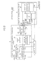
- - la Fig.3 montre en détail un circuit d'échantillonnage, un circuit de modulation et une base de temps inclus dans le modulateur ;
- - la Fig.4 sont des diagrammes temporels de signaux et impulsions établis dans le modulateur et le démodulateur respectivement ;
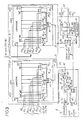
- - la Fig.5 montre en détail un circuit de détection et de validation d'impulsion reçue, inclus dans le démodulateur ; et
- - la Fig.6 montre un circuit de démodulation inclus dans le démodulateur.
- - Figs.1A and 1B are a schematic block diagram of a pulse duration modulator according to the invention, comprising a quantization circuit shown in detail;
- - Fig.2 is a block diagram of a demodulator according to the invention:
- - Fig.3 shows in detail a sampling circuit, a modulation circuit and a time base included in the modulator;
- - Fig.4 are time diagrams of signals and pulses established in the modulator and the demodulator respectively;
- - Fig.5 shows in detail a detection and validation circuit of received pulse, included in the demodulator; and
- - Fig.6 shows a demodulation circuit included in the demodulator.
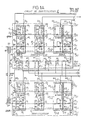
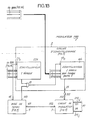
Dans les Figs.1A et 1B est représenté schématiquement un modulateur d'impulsions en durée MOD qui selon une première réalisation, est destiné à quantifier et échantillonner un signal modulant entrant analogique SE et à convertir des mots représentant des valeurs quantifiées du signal en des durées d'impulsion. Le signal modulant entrant est, d'une manière générale, un signal analogique qui peut être un signal de modulation en amplitude, en fréquence ou en phase, tel que par exemple un signal à basse fréquence du genre signal téléphonique. Le modulateur MOD comprend un circuit de quantification 1 pour quantifier instantanément le signal entrant de tension dans I.J intervalles de quantification, un circuit d'échantillonnage 2 pour prélever pendant une période d'échantillonnage T e un mot de quantification transmis par le circuit 2 et représentatif d'une valeur quantifiée du signal entrant, un circuit de modulation 3 pour convertir chaque valeur quantifiée en une durée d'impulsion modulant une porteuse, et une base de temps 4 commandant les circuits 2 et 3. Dans la Fig.2 est représenté un démodulateur DEM selon l'invention recevant des impulsions de différentes durées transmises par le circuit de modulation 3 à travers un moyen de transmission MT, par exemple tel que ligne téléphonique dans un réseau commuté téléphonique. Le démodulateur DEM comprend un circuit de détection et de validation 5 pour supprimer la porteuse, détecter les impulsions reçues et, de préférence, pour valider leur durée, un circuit de démodulation 6 pour convertir chaque impulsion détectée en un échantillon de tension dépendant de la durée de l'impulsion détectée, et une base de temps 7.In Figs. 1A and 1B is shown schematically a pulse modulator in duration MOD which according to a first embodiment, is intended to quantify and sample an incoming modulating analog analog signal SE and to convert words representing quantized values of the signal into durations impulse. The incoming modulating signal is, in general, an analog signal which can be an amplitude, frequency or phase modulation signal, such as for example a low frequency signal of the telephone signal type. The modulator MOD comprises a
Comme montré en détail à la Fig.1A, le circuit de quantification 1 est un circuit de quantification acyclique à vitesse de fonctionnement élevé tel celui décrit dans la demande de brevet français 86-00305 déposée le 10 janvier 1986 au nom de l'actuel demandeur. Le circuit 1 est partagé en deux quantificateurs QUA et qua par un transformateur différentiel d'entrée TD. Le signal entrant SE à quantifier est appliqué à un double enroulement primaire EP+ep du transformateur TD et est reproduit et polarisé positivement aux bornes de deux demi-enroulements secondaires ES et es du transformateur. Chacun des demi-enroulements secondaires ES, es a une borne portée à travers un potentiomètre PT, pt à une tension positive convenable VMOY correspondant une valeur moyenne de l'amplitude crête-à-crête du signal entrant. Les autres bornes des demi-enroulements ES et es constituent des bornes d'entrée BE, be des quantificateurs QUA et qua respectivement.As shown in detail in FIG. 1A, the
Le quantificateur QUA est destiné à quantifier le signal entrant dans une plage de quantification VT₀ à VT I partagée en I = 16 premiers intervalles de quantification de tension consécutifs VT₀,VT₁ à VT I-1, VT I respectivement associée à I premières cellules de quantification C₀ à C I-1 = C₁₅ Toutes les cellules sont identiques à l'exception de la première C₀ et de la dernière C I-1. Chacune des cellules C i de rangs i compris entre 1 et I-2 contient un circuit de détection CD i pour détecter une tension entrante supérieure à un niveau de décision définie par une tension limite inférieure VT i et comprise dans l'intervalle de quantification respectif VT i à VT i+1, et un circuit de signalisation CS i pour signaler par un état logique "1" à une borne de sortie BS i de la cellule une tension entrante comprise dans cet intervalle de quantification. La première cellule C₀ ne comprend qu'un circuit de signalisation CS₀ constitué par un simple inverseur IN₀, et la dernière cellule C I-1 contient un circuit de détection CD I-1analogue à ceux CD₁ à CD I-2 dans les cellules C₁ à C I-2, et un circuit de signalisation CS I-1 ne comprenant qu'une diode D3 I-1.The quantizer QUA is intended to quantify the signal entering a quantization range VT₀ to VT I shared at I = 16 first consecutive voltage quantization intervals VT₀, VT₁ to VT I-1 , VT I respectively associated with I first quantization cells C₀ to C I-1 = C₁₅ All cells are identical except for the first C₀ and the last C I-1 . Each of the cells C i of rows i between 1 and I-2 contains a detection circuit CD i for detecting an incoming voltage greater than a decision level defined by a lower limit voltage VT i and included in the respective quantization interval VT i to VT i + 1 , and a signaling circuit CS i for signaling by a logic state "1" to an output terminal BS i of the cell an incoming voltage included in this quantization interval. The first cell C₀ only comprises a signaling circuit CS₀ constituted by a simple inverter IN₀, and the last cell C I-1 contains a detection circuit CD I-1 similar to those CD₁ to CD I-2 in cells C₁ to C I-2 , and a signaling circuit CS I-1 comprising only one diode D3 I-1 .
Dans la cellule C i représentée en détail à la Fig.1A, le circuit de détection CD i comprend une résistance R2 i reliée en série avec d'autres telles résistan ces dans les cellules C₁ à C I-1entre des bornes à la masse et à une tension positive d'une source d'alimentation qui détermine la plage de quantification VT₀ = 0 à VT I du circuit de quantification 1. Les bornes des résistances R2₁ et R2 I-1 sont ainsi portées aux limites de tension VT₀ à VT I des intervalles de quantification. Par exemple dans la cellule C i, une borne T i de la résistance R2 i reliée à la résistance R2 i+1 dans la cellule de rang i+1 est portée à la tension VT i, laquelle est reportée à travers une diode D2 i à une borne S i d'un réseau de résistances et diodes en série. Ce dernier réseau comprend entre la borne d'entrée BE et l'anode de la diode D2 I-1 dans la cellule C I-1, des ensembles de diode et résisttance en série D1₁, R1₁ à D1 I-1, R1 I-1 ; dans une cellule C i, la résistance R1 i est connectée entre des émetteur et base d'un transistor bipolaire PNP TR i. Ainsi pour une tension à la borne BE, par exemple comprise sensiblement entre VT i et VT i+1, les diodes D1₁ à D1 i sont passantes et les transistors TR₁ à TR i sont activés, ou en d'autres termes, le transistor TR i est activé pour une tension à la borne BE excèdant la tension limite inférieure VT i de l'intervalle (VT i, VT i+1) associé à la cellule C i, grâce à la division de tension créée par le réseau de résistances R2₁ à R2 I-1 et le réseau de diodes et résistances R1₁ à R12 I-1 et D1₁ à D1 I-1. Il est à noter qu'en absence de signal entrant, la tension à la borne BE est ajustée à une tension moyenne sensiblement égale à VMOY et comprise dans l'intervalle de quantification (VT I/2-1, VT I/2) notamment lorsque la quantification est uniforme. Par ailleurs, les valeurs ohmiques des résistances peuvent être choisies pour réaliser une quantification uniforme, ou une quantification non uniforme déduite par exemple d'une fonction logarithmique connue du genre courbe de compression de niveaux de quantification pour modulations par impulsions codées du type MIC.In cell C i shown in detail in Fig. 1A, the detection circuit CD i comprises a resistor R2 i connected in series with other such resistors in cells C₁ to C I-1 between terminals to ground and at a positive voltage of a power source which determines the quantization range VT₀ = 0 to VT I of the
Dans le circuit de signalisation CS i, une porte ET P i a une première entrée reliée au collecteur du transistor TR i afin de mettre à "1" une borne de sortie BS i de la cellule C i uniquement lorsque la tension entrante à la borne BE est comprise entre VT i et VT i+1. Lorsque la tension entrante est inférieure à VT i, le transistor TR i est bloqué ce qui ferme la porte P i. Lorsque la tension entrante et supérieure à VT i+1, la borne de sortie de l'une des cellules C i+1 à C I-1 est activée à l'état "1" ce qui met à l'état "0" une seconde entrée de la porte P i à travers une diode de la cellule activée, équivalente à la diode D4 i dans la cellule C i, des diodes en série entre la cellule activée et la cellule C i, telles que la diode D3 i dans la cellule C i, et un inverseur IN idans la cellule C i.In the signaling circuit CS i , an AND gate P i has a first input connected to the collector of the transistor TR i in order to set to "1" an output terminal BS i of the cell C i only when the incoming voltage at the terminal BE is between VT i and VT i + 1 . When the incoming voltage is less than VT i , the transistor TR i is blocked, which closes the gate P i . When the incoming voltage and greater than VT i + 1 , the output terminal of one of the cells C i + 1 to C I-1 is activated in state "1" which puts in state "0" a second input of the gate P i through a diode of the activated cell, equivalent to the diode D4 i in the cell C i , diodes in series between the activated cell and the cell C i , such as the diode D3 i in cell C i , and an inverter IN i in cell C i .
Une tension du signal entrant polarisée comprise entre VT i et VT i+1 est signalée par l'état "1" à la borne de sortie BS i de la cellule C i et par l'état "0" aux bornes de sortie BS₀ à BS i-1 et BS i+1 à BS I-1 des autres cellules du quantificateur QUA.A voltage of the polarized incoming signal between VT i and VT i + 1 is signaled by the state "1" at the output terminal BS i of the cell C i and by the state "0" at the output terminals BS₀ to BS i-1 and BS i + 1 to BS I-1 of the other cells of the QUA quantizer.
Le second quantificateur qua affine la quantification du signal entrant dans les premiers intervalles (VT₀, VT₁) à (VT I-1, VT I) en divisant chacun d'eux en J seconds intervalles de quantification. Le quantificateur qua contient J secondes cellules c₀ à c J-1 agencées d'une manière analogue aux cellules C₀ à C I-1. Les cellules c₀, c₁ à c J-2 et c J-1 sont respectivement analogues aux cellules C₀, C₁ à C I-2 et C I-1. Dans la Fig.1, des composants inclus dans la cellule c j sont désignés par des repères ayant des lettres minuscules et des chiffres correspondant aux lettres majuscules et chiffres des repères désignant des composants équivalents dans la cellule C i. Les nombres I et J de cellules dans les quantificateurs QUA et qua peuvent être égaux ou différents.The second quantizer qua refines the quantization of the signal entering the first intervals (VT₀, VT₁) to (VT I-1 , VT I ) by dividing each of them into J second quantization intervals. The quantifier qua contains J second cells c₀ to c J-1 arranged in a manner analogous to cells C₀ to C I-1 . C₀, c₁ to c J-2 and c J-1 cells are respectively analogous to cells C₀, C₁ to C I-2 and C I-1 . In FIG. 1, components included in cell c j are designated by marks having lower case letters and numbers corresponding to capital letters and numbers of marks denoting equivalent components in cell C i . The cell numbers I and J in the quantifiers QUA and qua can be equal or different.
Le quantificateur qua comprend également des premier et second réseaux à diodes et résistances RDR1 et RDR2 pour appliquer sélectivement les tensions limites d'un premier intervalle de quantification lorsque la borne de sortie correspondante du premier quantificateur QUA est à l'état "1". Le premier réseau RDR1 applique à la résistance r2₁ de la cellule c₁ la tension inférieure du premier intervalle sélectionné à travers un potentiomètre ra1, tandis que le second réseau RDR2 applique à la résistance r2 J-1 de la cellule c J-1 la limite supérieure du premier intervalle sélectionné à travers un potentiomètre ra2. Ceci est réalisé dans le réseau RDR1 grâce à des divisions de tension obtenues par des résistances R4 I-1 à R4₀ reliées en série avec la résistance r2₁ et le potentiomètre ra1 et ayant des bornes respectives reliées aux bornes BS I-1 à BS₀ à travers des ensembles de diode D5 I-1 à D5₀ et inverseur INV1 I-1 à INV₀, et dans le réseau RDR2, grâce à des divisions de tension obtenues par des résistances R5₀ à R5 I-1reliées en série avec la résistance r2 J-1 et le potentiomètre ra2 et ayant des bornes respectives reliées aux bornes BS₀ à BS I-1 à travers des diodes D6₀ à D6 I-1 polarisées en inverse comparativement aux diodes D5₀ à D5 I-1.The quantizer qua also includes first and second diode networks and resistors RDR1 and RDR2 for selectively applying the limit voltages of a first quantization interval when the corresponding output terminal of the first quantizer QUA is in the state "1". The first network RDR1 applies to the resistance r2₁ of the cell c₁ the lower voltage of the first interval selected through a potentiometer ra1, while the second network RDR2 applies to the resistance r2 J-1 of cell c J-1 the upper limit of the first interval selected through a potentiometer ra2. This is achieved in the RDR1 network thanks to voltage divisions obtained by resistors R4 I-1 to R4₀ connected in series with the resistor r2₁ and the potentiometer ra1 and having respective terminals connected to the terminals BS I-1 to BS₀ through diode assemblies D5 I-1 to D5 invers and inverter INV1 I-1 to INV₀, and in the network RDR2, thanks to voltage divisions obtained by resistors R5₀ to R5 I-1 connected in series with the resistor r2 J- 1 and the potentiometer ra2 and having respective terminals connected to the terminals BS₀ to BS I-1 through diodes D6₀ to D6 I-1 reverse biased compared to the diodes D5₀ to D5 I-1 .
Lorsque la borne BS i est à l'état "1", l'intervalle (VT i, VT i+1) est partagé en J seconds intervalles consécutifs (vt 0,i = VT i, vt 1,i), (vt 1,i,vt 2,i) à (vt J-2,i, vt J-1,i) et (vt J-1,i, vt J,i = VT i+1), les tensions limites vt 1,i à vt J-1,i étant appliquées aux bornes t₁ à t J-1 des résistances r2₁ à r2 J-1 dans les cellules c₁ à c J-1.When the terminal BS i is in the state "1", the interval (VT i , VT i + 1 ) is divided into J second consecutive intervals (vt 0, i = VT i , vt 1, i ), (vt 1, i , vt 2, i ) to (vt J-2, i , vt J-1, i ) and (vt J-1, i , vt J, i = VT i + 1 ), the limit voltages vt 1 , i to vt J-1, i being applied to the terminals t₁ to t J-1 of the resistors r2₁ to r2 J-1 in the cells c₁ to c J-1 .
A un instant donné, une quantification de la tension instantanée du signal entrant polarisé est marquée par deux bornes de sortie BS i et bs j des quantificateurs QUA et qua à l'état "1" parmi I.J = niveaux de quantification possibles. En d'autres termes, une valeur quantifiée de la tension instantanée du signal entrant est représentée par un mot de quantification à un instant donné composé d'une première partie ayant I-1 bits à l'état "0" et un bit à l'état "1" délivrés en parallèle par les sorties BS₀ à BS I-1 et d'une seconde partie ayant J-1 bits à l'état "0" et un bit à l'état "1" délivrés en parallèle par les sorties bs₀ à bs J-1. Par exemple, afin de fixer les idées, les nombres I et J sont supposés égaux à 16 dans la suite, ce qui correspondant à une quantification du signal entrant dans 256 intervalles de quantification.At a given instant, a quantization of the instantaneous voltage of the polarized incoming signal is marked by two output terminals BS i and bs j of the quantizers QUA and qua in the state "1" among IJ = possible quantization levels. In other words, a quantized value of the instantaneous voltage of the incoming signal is represented by a quantization word at a given instant composed of a first part having I-1 bits in the "0" state and a bit at l 'state "1" delivered in parallel by the outputs BS₀ to BS I-1 and of a second part having J-1 bits in the state "0" and a bit in the state "1" delivered in parallel by the outputs bs₀ to bs J-1 . For example, in order to fix the ideas, the numbers I and J are assumed to be equal to 16 below, which corresponds to a quantization of the signal entering 256 quantization intervals.
En référence à la Fig.3, le circuit d'échantillonnage 2 comprend deux échantillonneurs ECH et ech respectivement associés aux quantificateurs QUA et qua qui analysent périodiquement les états des sorties BS₀ à BS I-1 et bs₀ à bs J-1 et ainsi prélèvent des mots de quantification à I+J bits à une fréquence d'échantillonnage F e=1/T e afin de les convertir en des impulsions ayant une largeur prédéterminée T₀ et des positions dans les périodes d'échantillonnage fonction des valeurs quantifiées du signal entrant. Le circuit d'échantillonage 2 opère ainsi une modulation d'impulsions en position.With reference to FIG. 3, the
Chaque échantillonneur ECH, ech comporte un compteur COM, com ayant I=J=16 étages remis à zéro par bouclage sur lui-même, et I,J portes ET à deux entrées PE₀ à PE I-1, pe₀ à pe J-1. Les portes PE₀ à PE I-1 ont des premières entrées reliées aux bornes de sortie BS₀ à BS I-1 du premier quantificateur QUA, des secondes entrées reliées aux sorties des I étages du compteur COM, et des sorties reliées à I entrées d'une porte OU PO, respectivement. La porte PO a une sortie reliée à une première entrée 211 d'une porte ET 21 ayant une sortie reliée à une entrée d'horloge eh₀ du compteur com. De même, les portes pe₀ à pe J-1 ont des premières entrées reliées aux bornes de sortie bs₀ à bs J-1 du second quantificateur qua, des secondes entrées reliées aux sorties des J étages du compteur com, et des sorties reliées à J entrées d'une porte OU po, respectivement.Each ECH, ech sampler has a COM counter, com having I = J = 16 stages reset to zero by looping back on itself, and I, J doors AND with two inputs PE₀ to PE I-1 , pe₀ to pe J-1 . The gates PE₀ to PE I-1 have first inputs connected to the output terminals BS₀ to BS I-1 of the first quantizer QUA, second inputs connected to the outputs of the I stages of the counter COM, and outputs connected to I input of an OR gate, respectively. The gate PO has an output connected to a
Comme montré également à la Fig.3, la base de temps 4 comprend une horloge 41, un compteur 42 de préférence programmable, une bascule du type D 43, une porte ET à deux entrées 44 et un diviseur de fréquence par J 45.As also shown in FIG. 3, the
La base de temps 4 est destinée à prélever deux bits tels que BS i="1" et bs j="1" dans les échantillonneurs ECH et ech pendant une période d'échantillonnage T e et à commander la conversion d'une impulsion ayant une largeur égale à une période d'horloge T₀ sortant du circuit 2 en une impulsion IM1 ij ayant une durée d1 ijqui est inférieure à une durée maximale d M elle-même inférieure à T e et qui dépend de la position temporelle de l'impulsion sortant du circuit 2 dans une période T e, comme montré à une troisième ligne dans la Fig.4. Une période d'échantillonnage T e débutant à un instant ϑ₀ est décomposée en trois durées consécutives d₁₂, d M et d m commençant respectivement à des instants ϑ₀, ϑ₂, et ϑ M et finissant respectivement à des instants ϑ₂=ϑ₀+d₁₂, ϑ M=ϑ₀+d₁₂+d M et ϑ₀+T e. L'instant ϑ₂ détermine le début de transmission d'une impulsion IM1 ij par le circuit de modulation 3. L'impulsion IM1 ij a une durée d1 ij qui est fonction des rangs i et j des bits BS i et bs j à l'état "1" dans le mot de quantification prélevé et inférieure ou égale à d M, et donc qui est proportionnelle à la valeur instantanée du signal entrant SE. La durée d M est celle d'une impulsion IM1 I-1,J-1 ayant la durée maximale et correspondant à l'amplitude maximale crête-à-crête du signal entrant et donc à un mot de quantification avec des bits BS I-1=BS₁₅="1" et bs J-1=bs₁₅="1". Ainsi, sous la commande d'un signal d'horloge h₀ de période T₀, le compteur COM doit lire les bornes BS₀ à BS I-1pendant la durée d M dans chaque période d'échantillonnage T e, et le compteur com doit lire les bornes bs₀ à bs J-1 pendant la durée d'analyse de l'une des bornes BS₀ à BS I-1 à l'état "1". En conséquence, pendant une période d'échantillonnage, le compteur COM effectue un cycle de durée égale à d M = I.J.T₀ = 256.T₀ = T e-d₁₂-d m& , et le compteur com effectue un cycle de durée égale à d M/I=JT₀=16T₀.The
Le compteur 42 et la bascule 43 dans la base de temps 4 élaborent des impulsions de durée d M positionnées dans les périodes T e comme montré à une seconde ligne de la Fig.4. A cette fin, une entrée d'horloge 42H du compteur 42 reçoit le signal d'horloge h₀ délivré par l'horloge 41. Une sortie 421 du compteur 42 est reliée à une entrée d'horloge 43H de la bascule 43 et passe à "1" après une durée d₁₂ succédant au début ϑ₀ d'une période d'échantillonnage T e, comme montré à une première ligne de la Fig.4. Une entrée 43D de la bascule 43 étant en permanence à l'état "1", une sortie 43Q de celle-ci produit alors une impulsion de durée d M à partir de l'instant ϑ₂ de la période T e, impulsion dont le front descendant est obtenu lorsqu'une sortie 42M du compteur 42 met à "1" une entrée de remise à zéro 43R de la bascule 43, en réponse à un comptage de I.J impulsions d'horloge succédant à l'instant ϑ₂. Puis après un comptage d'impulsions d'horloge h₀ pendant une durée égale à d m, une sortie 42m du compteur 42 reliée à une entrée de remise à zéro 42R de celui-ci passe à "1" afin de remettre à zéro le compteur et les sorties 421, 42M et 42m et d'établir une nouvelle période d'échantillonnage.The
A titre d'exemple, la durée d₁₂ est égale à T e/9, et la durée d m est égale à 0, les sorties 42M et 42m étant confondues, ou est par exemple égale à T₀, et est considérée dans la suite comme négligeable par rapport aux durées d₁₂ et d M, celles-ci étant pratiquement complémentaires dans la période T e. Ainsi le compteur 42 met à "1" la sortie 421 après un comptage de 256/8=32 impulsions d'horloge succédant à l'instant ϑ₀, et met à "1" la sortie 42 Maprès un comptage de 32+256=288 impulsions d'horloge succédant à l'instant ϑ₀.For example, the duration d₁₂ is equal to T e / 9, and the duration d m is equal to 0, the
La porte ET 44 a une première entrée 441 recevant les impulsions d'horloge h₀ de période T₀ et une seconde entrée 442 reliée à la sortie 43Q de la bascule 43 afin de produire en une sortie 443, I.J=256 impulsions d'horloge pendant la durée d M de chaque période d'échantillonnage T e. Ces I.J impulsions d'horloge sont appliquées à une entrée du diviseur de fréquence 45 et à une seconde entrée 212 de la porte ET 21.The AND
Le diviseur 45 fournit I=16 impulsions à une période de JT₀ pendant la durée d M à une entrée d'horloge EH₀ du compteur COM qui est activé pour un cycle. Pendant ce cycle de durée d M, le compteur COM ouvre successivement les portes PE₀ à PE I-1 pour lire les I bornes de sortie BS₀ à BS I-1 du quantificateur QUA et ainsi détecter l'état "1" de l'une de ces bornes, telle qu'une borne BS i, en réponse à l'impulsion d'horloge de rang i+1 appliquée à l'entrée EH₀ à partir de l'instant ϑ₂. A travers le compteur COM et la porte OU PO, cette impulsion de rang i+1 ouvre la porte 21 pendant une durée égale à JT₀ succédant à une durée iJT₀ à partir de l'instant ϑ₂ dans la période d'échantillonnage T e en cours. Un groupe de J impulsions d'horloge consécutives de période T₀ est alors appliqué à l'entrée d'horloge eh₀ du compteur com par la sortie 213 de la porte 21. Les J impulsions d'horloge sont comptées dans le compteur com qui ouvre successivement les portes pe₀ à pe N-1 pour balayer les J bornes de sortie bs₀ à bs J-1 du quantificateur qua et ainsi détecter l'état "1" de l'une de ces bornes, telle qu'une borne bs j, en réponse à l'impulsion d'horloge de rang j+1 appliquée à l'entrée eh₀ pendant la durée JT₀. Une sortie 23 de la porte OU po produit une impulsion de largeur T₀ après une durée d1 ij-T₀ = iJT₀ ϑ→₀ à partir de l'instant ϑ₂ de la période d'échantillonnage T e en cours. La durée d₁₂+d1 ij - T₀ détermine la position temporelle du front montant de l'impulsion d'horloge sortant de la porte po dans une période T e. La durée d1 ij = iJT₀+(j+1)T₀ est égale à la largeur d'une impulsion modulée IM1 ij obtenue dans le circuit de modulation 3 et correspondant au codage en durée d'impulsion du mot de quantification prélevé en sortie du circuit 2 et donc du niveau instantané du signal entrant sur une échelle de I.J=256 niveaux de quantification.The
A l'issue de chacun des cycles de balayage respectifs de I=J=16 bornes, soit à l'expiration d'une durée égale à IJT₀, JT₀ pendant la durée d M, les compteurs COM et com ont leur compte remis à zéro et demeurent à cet état pendant la durée d₁₂ de la période d'échantillonnage suivante, jusqu'à ce que la porte ET 44 soit ouverte. Comme on le verra dans la suite, pendant la durée d₁₂, une impulsion modulée est convertie en amplitude et est effacée d'une mémoire, telle que condensateur, dans le démodulateur DEM.At the end of each of the respective scanning cycles of I = J = 16 terminals, that is to say at the expiration of a duration equal to IJT₀, JT₀ during the duration d M , the counters COM and com have their count reset and remain in this state for the duration d₁₂ of the following sampling period, until the AND
Comme montré également à la Fig.3, le circuit de modulation 3 comprend une bascule bistable 30, un inverseur 300, une porte ET à deux entrées 31, une porte ET à trois entrées 32, un inverseur 33 et un générateur 34 générant, de préférence à partir de la fréquence d'horloge 1/T₀, deux porteuses de fréquence fp₁ et fp₂, de préférence très voisines, par des sorties 341 et 342. La bascule 30 a une entrée de mise à "1" 30S reliée à la sortie 421 du compteur 42, ou à l'entrée 442 de la porte 42. Une entrée de remise à "0" 30R de la bascule 30 est reliée à la sortie 23 de la porte OU po à travers l'inverseur 300. Une sortie 30Q de la bascule 30 fournit une impulsion modulée IM1 ij ayant une durée d1 ij=iJT₀+(j+1)T₀ lorsque l'état "1" est détecté aux bornes BS i et bs j pendant une période d'échantillonnage T e. Le front avant montant d'une telle impulsion IM1 ij, quels que soient i et j, est toujours positionné à l'instant ϑ₂ dans une période d'échantillonnage T e, comme montré à une troisième ligne de la Fig.4. Ainsi, au cours d'une période d'échantillonnage et malgré la variation instantanée des indices i et j, le circuit de modulation 3 code le premier niveau de quantification rencontré en une impulsion. La sortie 30Q de la bascule 30 est remise à zéro par le front arrière descendant de l'impulsion d'horloge à la borne 23 et donc aussitôt remise à zéro après l'impulsion IM1 ij jusqu'à la fin de la période d'échantillonnage. La modulation est donc univoque entre un couple de bits BS i et bs j à l'état "1" et une impulsion IM1 ij.As also shown in FIG. 3, the
L'impulsion IM1 ij obtenue à la sortie 30Q ouvre la porte 31 ayant des entrées reliées aux bornes 30Q et 341. Une sortie 311 de la porte ET 31 transmet l'impulsion IM1 ij modulant la fréquence porteuse fp₁ pendant la durée d1 ij. De préférence pour des raisons concernant un contrôle à la réception dans le démodulateur DEM, une sortie 321 de la porte ET 32 délivre une impulsion IM2 ij modulant la fréquence porteuse fp₂ et ayant une durée d2 ij égale au complément de la durée d1 ij pendant la durée d M de la période d'échantillonnage, ou plus généralement pendant la durée d M+d m, soit d2 ij=d M+d m-d1 ij, l'impulsion IM2 ij ayant toujours un front descendant positionné à la fin d'une période T e, comme montré à une quatrième ligne de la Fig.4. A cette fin, les trois entrées de la porte 32 sont respectivement reliées à la sortie 421 du compteur 42 dans la base de temps, à la sortie 3 0Q de la bascule 30 à travers l'inverseur 33, et à la sortie 342 du générateur 34. Dans ce cas, le moyen de transmission MT convoie dans deux lignes parallèles les impulsions IM1 ij et IM2 ij multiplexées en fréquence. Comme on le verra dans la suite, la réception des paires d'impulsions successives IM1 ij et IM2 ij permet de tester la conformité du signal reçu en vérifiant que la somme des durées de deux impulsions "complémentaires" est toujours constante et égale à d M, ou d M+d m, pendant chaque période d'échantillonnage T e.The pulse IM1 ij obtained at output 30Q opens the
Selon une autre variante du modulateur, celui-ci ne comprend qu'un quantificateur QUA et un échantillonneur ECH lorsque le nombre de niveaux de quantification est faible ; dans ce cas, la sortie de la porte OU PO (Fig.3) est reliée directement à l'entrée 30R de la bascule 30 à travers l'inverseur 300.According to another variant of the modulator, it only comprises a quantizer QUA and a sampler ECH when the number of quantization levels is small; in this case, the output of the OR gate PO (Fig.3) is directly connected to the
Le démodulateur DEM est maintenant décrit en référence aux Figs.2, 5 et 6.The DEM demodulator is now described with reference to Figs. 2, 5 and 6.
Après amplification dans des moyens d'entrée connus et non représentés du démodulateur, des impulsions IM1 ij et IM2 ij modulant les fréquences porteuses fp₁ et fp₂ sont respectivement reçues à des entrées 501₁ et 501₂ de deux détecteurs de porteuse 50₁ et 50₂ inclus dans le circuit de détection et validation d'impulsion 5 montré à la Fig.5. Les détecteurs 50₁ et 50₂ sont de préférence des dispositifs de détection d'impulsions en fonction de leur durée du genre décrit dans la demande de brevet français 85-15418 déposée le 17 Octobre 1985, au nom de l'actuel demandeur. Ces détecteurs 50₁ et 50₂ sont programmés par la base de temps 7 pour détecter des alternances de sinusoïdes de largeurs 1/(2fp₁) et 1/(2fp₂) et ainsi restituer des tensions continues en réponse aux porteuses fp₁ et fp₂ pendant les durées d1 ij et d2 ij des impulsions IM1 ij et IM2 ijrespectivement. Des sorties 502₁ et 502₂ restituent ainsi deux impulsions IM1 ij et IM2 ij sans porteuse, dans chaque période d'échantillonnage T e.After amplification in known and not shown input means of the demodulator, pulses IM1 ij and IM2 ij modulating the carrier frequencies fp₁ and fp₂ are respectively received at
Le circuit 5 comprend également un circuit de vérification de complémentarité 51, un circuit de sélection d'impulsions complémentaires 52 et un circuit de commande 53 en sortie.The
Le circuit de vérification de complémentarité 51 comprend une porte OU-Exclusif 511 ayant deux entrées respectivement reliées aux bornes 502₁ et 502₂, un dispositif de détection d'impulsion 512 relié à la sortie de la porte 511, une porte ET 513 ayant une première entrée reliée directement à la sortie 514 du dispositif 512 et une seconde entrée reliée à la sortie 502₁ à travers une ligne à retard 521₁, et un inverseur 515 relié à la sortie 514 du dispositif 512. Lorsque pendant une période d'échantillonnage, deux impulsions IM1 ij et IM2 ij ont des fronts respectifs descendant et montant simultanés et donc sont consécutives, la sortie de la porte 511 transmet une unique impulsion de durée d M, ou d M+d m, à l'entrée du dispositif 512. Le dispositif 512 est du genre de celui décrit dans la demande de brevet précitée 85-15418, et est programmé par la base de temps 7 pour détecter des impulsions de largeur d M, ou d M+d m, à la période T e, c'est-à-dire pour détecter des impulsions périodiques de largeur d M, ou d M+d m, espacées d'un écart temporel égal à d₁₂. La sortie 514 du dispositif 512 est à l'état "1" tant que des impulsions à la sortie de la porte 511 ont des largeurs de d M, ou d M+d m, et des écarts temporels entre elles de d₁₂, c'est-à-dire tant que des impulsions IM1 ij et IM2 ij sont rigoureusement complémentaires p endant la durée d M, ou d M+d m, dans les périodes T e. Dans ce cas, la porte ET 513 est ouverte pour transmettre les impulsions IM1 ij appliquées par la ligne à retard 521₁ vers une entrée 532 C d'une porte OU à trois entrées 531 incluse dans le circuit de commande 53. Selon une autre variante non illustrée, au lieu de transmettre les impulsions IM1 ij, les impulsions IM2 ij sont transmises par la porte 513 en reliant l'entrée de la ligne à retard 521₁ à la sortie 502₂ du détecteur 50₂, ou en reliant la seconde entrée de la porte 513 uniquement à la sortie 502₂ à travers une ligne à retard 521₂. La ligne à retard 521₁, comme l'autre ligne à retard 521₂ dans le circuit de sélection 52, impose un retard égal à d M ou d M+d m, ou égal à 2d M+T eou à 2(d M+d m)+T e selon le type choisi du dispositif 512 afin de compenser le retard imposé par la détection d'impulsions de durée d M, ou d M+d m dans le dispositif 512. Dans la suite, comme déjà dit, on considère que d m est égal à 0, ou que d M peut être remplacé par d M+d m.The
Dans le cas où la complémentarité de deux impulsions IM1 ij et IM2 ij n'est pas reconnue dans le dispositif 512, la porte 513 est fermée et une sortie de l'inverseur 515 active une porte ET à trois entrées 523 et une porte ET à deux entrées 524 incluses dans le circuit de sélection 52. Deux conditions sont alors à distinguer en l'absence de complémentarité d'impulsions.In the case where the complementarity of two pulses IM1 ij and IM2 ij is not recognized in the
Selon une première condition, l'absence de complémentarité est due à un allongement ou à un raccourcissement de la durée de l'une des impulsions détectées IM1 ij et IM2 ij. A cause de cette situation indéterminée, le signal reçu est alors éliminé par fermeture de la porte ET 524 grâce à deux bascules monostables 525₁ et 525₂ interconnectées respectivement entre les bornes 501₁ et 501₂ et deux autres entrées de la porte ET 523 ayant une sortie reliée à une seconde entrée de la porte 524 à travers un inverseur 526. Les bascules monostables ont des constantes de temps égales à T e et sont redéclenchables par les fronts avant montants des impulsions IM1 ij et IM2 ij respectivement, de sorte qu'en présence d'impulsions successives et non consécutives IM1 ij et IM2 ij, la porte 523 est ouverte et ferme la porte 524 qui ferme à son tour deux portes ET à deux entrées 527₁ et 527₂. Selon la réalisation illustrée à la Fig.5, les portes ET 527₁ et 527₂ reçoivent par des secondes entrées les impulsions IM1 ij et IM2 ij à travers les lignes à retard 521₁ et 521₂ et ont des sorties reliées aux deux autres entrées 532₁ et 532₂ de la porte OU 531, respectivement. Dans le cas de liaisons télématiques, la sortie de la porte 523 à l'état "1" peut commander l'envoi en arrière, vers la partie de transmission comprenant le modulateur, d'un signal demandant la répétition d'une partie du message, telle que dernier caractère ou octet transmis.According to a first condition, the absence of complementarity is due to an lengthening or a shortening of the duration of one of the detected pulses IM1 ij and IM2 ij . Because of this indeterminate situation, the received signal is then eliminated by closing the AND
Selon une seconde condition, la complémentarité n'est pas constatée par la porte OU-Exclusif 511 et le dispositif 512, et l'une des impulsions IM1 ij et IM2 ij n'est pas détectée par les détecteurs 50₁ et 50₂. Ceci se traduit par un état "0" à l'une des bornes 502₁ et 502₂ pendant au moins une période d'échantillonnage T e, et en pratique, pendant plusieurs périodes T e lorsque l'un des moyens de transmission des impulsions IM1 ij et IM2 ij entre le modulateur MOD et le démodulateur DEM est perturbé, par exemple d û au fading sur une porteuse. Dans ce cas, l'une des bascules monostables 525₁ et 525₂ n'est pas déclenchée ce qui ferme la porte 523 et ouvre la porte 524 qui commande le passage de l'impulsion détectée IM1 ij ou IM2 ij à travers la porte ET ouverte respective 527₁ ou 527₂. Comme on le verra dans la suite, la démodulation des impulsions IM1 ij et celle des impulsions IM2 ij conduisent à des signaux en opposition de phase ce qui, dans le cas général et dans la mesure où la perturbation est faible, est sans effet sur une restitution phonique ou numérique du signal démodulé.According to a second condition, the complementarity is not observed by the Exclusive-OR gate 511 and the
Le circuit de commande 53 comprend, outre la porte OU 531, deux portes 533 et 534 ayant respectivement des premières entrées reliées à la borne 502₁ à travers la ligne à retard 521₁, et à la sortie de la porte OU 531, des secondes entrées reliées à travers un inverseur 535 et directement à une borne de commande 5C, et des sorties reliées à une borne d'entrée 6E du circuit de démodulation 6 à travers une porte OU à deux entrées 536. Au moyen d'un interrupteur ou de tout autre dispositif de commande, la borne de commande 5C à l'état "1" met en service les circuits 51 et 52 du circuit de détection et de validation 5 en ouvrant la porte 534 et en fermant la porte 533 afin de transmettre à travers la porte OU 531 des premières impulsions IM1 ij validées par le dispositif 512 ou des impulsions sélectionnées parmi des impulsions IM1 ij et IM2 ijdétectées par le circuit 52. Dans le cas où aucun contrôle des impulsions n'est désiré, la borne 5C est à l'état "0", la porte 534 est fermée et la porte 533 est ouverte pour transmettre directement des impulsions non contrôlées IM1 ij sans porteuse délivrées par la borne 502₁ à travers la ligne à retard 521₁.The
Comme montré à la Fig.6, le circuit de démodulation 6 comprend une bascule bistable 61 pour détecter les fronts montants des impulsions IM1 ij, auxquelles on se référa dans la suite, ou éventuellement des impulsions IM2 ij, reçues à l'entrée 6E, un circuit de reproduction d'échantillons du signal entrant 62, et un circuit de commande 63 pour prélever des échantillons.As shown in FIG. 6, the
Le circuit de reproduction d'échantillons 62 comprend essentiellement un condensateur 621 qui, pendant chaque période d'échantillonnage, est chargé par une tension fonction de la largeur d'une impulsion IM1 ij reçue pendant cette période, puis est déchargé complètement, et un élément à résistivité variable sous la forme d'un transistor à effet de champ à impédance d'entrée élevée du type transistor unijonction 622 qui est alimenté par la tension mémorisée par le condensateur 621 et donc proportionnelle à la durée d1 ij de l'impulsion reçue IM1 ij et au niveau de tension quantifiée correspondant du signal entrant SE et établi dans le circuit de quantification 1. Le condensateur 621 a une armature portée à la terre et une autre armature A qui est reliée à l'émetteur E de conductibilité P du transistor 622, à la cathode d'une diode 623 à travers une résistance ajustable 624, et à l'anode d'une diode 625. L'anode de la diode 623 est reliée à la borne d'entrée 6E et à une borne de mise à "1" 61S de la bascule 61. Des bases B₁ et B₂ du transistor 622 sont respectivement connectées à la terre et à une borne de sortie 6S du circuit de démodulation reliée à une borne de résistance ajustable 626.The
Le circuit de commande 63 comprend trois portes ET à deux entrées 631, 632 et 633, un compteur 634 et une bascule monostable déclenchable par front descendant 635. Des premières entrées des portes 631, 632 et 633 sont reliées à une sortie 61Q de la bascule bistable 61 afin que ces trois portes soient activées en réponse à un front montant d'une impulsion IM1 ij détectée à l'entrée 6E par la bascule 61.The
Une borne de sortie 71 de la base de temps 7 fourni t à une seconde entrée de la porte 631 un signal d'horloge permettant au compteur 634 d'établir la durée d M et des durées d₁ et d₂ telles que d₁+d₂ = d₁₂ pendant une période T e. On suppose que, selon l'exemple déjà choisi pour lequel d₁₂=T e/9, les durées d₁ et d₂ sont égales à T e/18 définissant la période du signal sortant de la borne 71. Un tel signal d'horloge peut être obtenu à partir d'une horloge fournissant un signal d'horloge de période T₀ à partir duquel la base de temps 7, établit également, au moyen de diviseurs de fréquence programmables, des fréquences d'horloge nécessaires aux dispositifs de détection d'impulsions 50₁, 50₂ et 512 dans le circuit de détection et de validation 5. La base de temps 7 est complètement indépendante de la base de temps 4 dans le modulateur MOD et, par conséquent, les opérations de modulation et démodulation sont asynchrones et ne nécessitent pas un quelconque circuit de récupération d'horloge dans le démodulateur DEM grâce aux dispositifs 50₁, 50₂ et 512.An
Le compteur 634 comprend ici cinq étages et reçoit à une entrée d'horloge 634H le signal d'horloge de période d₁ à travers la porte 631. Une première sortie 634 M du compteur 634 est reliée à une seconde entrée de la porte 632 ayant une sortie reliée à travers la résistance 626 à la borne 6S et donc à la base de commande B₂ du transistor 622. Une seconde sortie 634₁ du compteur 634 est reliée d'une part à une seconde entrée de la porte 633 ayant une sortie reliée à la cathode de la diode 625 à travers un inverseur 636, d'autre part à une entrée 635S de la bascule monostable 635 ayant une sortie 635Q reliée à des entrées de remise à zéro 61R et 634R de la bascule 61 et du compteur 634.The
En réponse au front avant montant d'une impulsion reçue IM1 ijdétectée par la bascule 61, marquant le début ϑ₂ d'une période d'échantillonnage T e dans le circuit 6, le compteur 634 est activé par des impulsions d'horloge de période d₁=d₂ traversant la porte ouverte 631. Les sorties 634 M et 634₁ demeurent à l'état "0" jusqu'à ce que le compteur 634 ait décompté une durée d M. Pendant cette durée d M, la porte 632 est bloquée et offre une sortie à la terre pour bloquer le transistor unijonction 622 et conserver ainsi une tension nulle à la borne 6S. De même, la porte 633 est bloquée et sa sortie est à "0" ce qui bloque la diode 625 à travers l'inverseur 636 et permet une charge du condensateur 621 à travers la diode 623 et la résistance 624. La résistance 624 est ajustée préalablement afin que la courbe de charge du condensateur 621 pour une durée égale ou inférieure à d M soit sensiblement une droite. Dans ces conditions, le condensateur 621 est chargé pendant la durée d1 ij de l'impulsion IM1 ij qui est normallement inférieure ou égale à d M. A l'issue de la durée décomptée d M correspondant à la plus longue durée des impulsions reçues, la sortie 634 M du compteur passe à "1" ce qui ouvre la porte 632 et débloque le transistor 622 pendant une durée d₁ succédant à d M, la porte 633 étant encore fermée. Pendant cette durée d₁, c'est-à-dire entre des instants ![]()
![]()
A l'expiration ϑ₂+d M+d₁ de la durée d₁, la sortie 634 M passe à "0" ce qui ferme la porte 632, bloque le transistor 622 et met la borne 6S au potentiel de 0 volt, et la sortie 634₁ passe à "1" pendant une durée d₂ pour ouvrir la porte 633 et décharger complètement le condensateur 621 à travers la diode passante 625. Après cette période d'effacement d₂ de la tension de charge du condensateur 621, un passage de "1" à "0" de la borne 634₁ est détecté par la bascule monostable 635 qui remet à "0" la bascule 61 et le compteur 634 qui sont de nouveau prêts pour convertir la durée d1 ij d'une autre impulsion IM1 ij en un échantillon de tension e ij pendant la prochaine période d'échantillonnage.At the expiration ϑ₂ + d M + d₁ of the duration d₁, the
Les échantillons e ij de durée d₁ à la borne 6S sont ensuite amplifiés et lissés dans des moyens connus pour restituer le signal analogique SE entrant initialement dans le modulateur MOD.The samples e ij of duration d₁ at terminal 6S are then amplified and smoothed in known means to restore the analog signal SE initially entering the modulator MOD.
D'une manière analogue à une utilisation du circuit de quantification 1 pour convertir plusieurs signaux analogiques, tels que signaux téléphoniques reçus en parallèle en des signaux numériques, décrite dans la demande de brevet français 86-00305, le circuit de quantification 1 peut être utilisé pour convertir N signaux analogiques SE₁ à SE N en des impulsions modulées en durée. Dans ce cas, la base de temps 4 produit des signaux d'adressage vers des circuits de commutation pour sélectionner successivement des échantillons des N signaux analogiques pendant un cycle de durée NT e qui sont quantifiés dans le circuit 1 et convertis en impulsions modulées en durée par le circuit d'échantillonnage 2 et la bascule 30. La sortie 30Q de la bascule est reliée à N paires de portes ET 31₁, 32₁ à 31 N, 32 N, telles que les portes 31 et 32, qui sont ouvertes successivement par les signaux d'adressage. Dans ce cas, les paires de porte ET 31₁, 32₁ à 31 N, 32 N reçoivent respectivement des paires de porteuses différentes f p₁₁, f p₂₁ à f p1N, f p2N. Par exemple, les plus faibles fréquences porteuses sont sensiblement supérieures à la fréquence du signal d'horloge h₀. A la réception, N démodulateurs selon l'invention démodulent les impulsions modulant les fréquences porteuses en les signaux SE₁ à SE N respectivement.In a manner analogous to a use of the
Pour cette utilisation, si les compteurs COM et com fonctionnent avec la plus grande fréquence d'horloge des compteurs actuels, soit 1/T₀≅25 MHz, un cycle d'exploration de I.J = 256 niveaux de quantification pour l'un des N signaux analogiques a une durée minimale de 256 (10⁻⁶/25) = 10,24 µs. Cette durée est égale à d M = 8T e/9 selon l'exemple déjà évoqué, ce qui correspond à une période d'échantillonnage T e = 9.10,24/8 = 11,52 µs, avec d₁ = d₂ = T e/9. Pour un cycle de sélection à 8 kHz, les signaux analogiques tels que signaux téléphoniques sont en nombre égal à :
N≅125/11,52 soit N = 10 voies téléphoniques.For this use, if the COM and com counters operate with the highest clock frequency of the current counters,
N≅125 / 11.52 or N = 10 telephone channels.
Cette multiple modulation permet par exemple une injection directe dans une ligne téléphonique d'abonné, d'impulsions modulées en durée à travers un équipement de signalisation de ligne d'abonné pour commutateur téléphonique, tel que décrit dans la demande de brevet français FR-A-2 585 526 au nom de l'actuel demandeur ; les signaux injectés sous forme d'impulsions concernent notamment de la signalisation téléphonique, de la parole artificielle et de la modulation téléphonique proprement dite.This multiple modulation allows for example a direct injection into a subscriber telephone line, of pulses modulated in duration through a subscriber line signaling equipment for telephone switch, as described in the French patent application FR-A -2 585 526 in the name of the current applicant; the signals injected in the form of pulses relate in particular to telephone signaling, artificial speech and telephone modulation proper.
Selon une seconde utilisation des modulateur et démodulateur d'impulsions en durée, le signal entrant est un signal numérique, tel qu'un signal MIC à 2048 kbit/s convoyant trente-deux voies. Chacune des voies multiplexées a un octet occupant une fenêtre temporelle de 3,9 µs dans une trame de 125 µs. Pour cette seconde utilisation, le circuit de quantification 1 est remplacé par un convèrtisseur série-parallèle et un circuit de transcodage pour convertir chaque octet de voie dans le signal MIC en un mot de quantification selon l'invention ayant I+J = 16+16 = 32 bits appliqué au circuit d'échantillonnage à la période de T e = 3,9 µs. Le circuit de transcodage peut comprendre des mémoires ou des compteurs. Un circuit de récupération classique de signal d'horloge à la fréquence de 2048 kHz et de fréquence trame de 8 kHz permet de commander le circuit de transcodage et de fournir la fréquence 1/T₀ à la base de temps 4. Lorsque l'octet MIC est transcodé en impulsion codée en durée (256 niveaux), on peut faire bénéficier le système MIC d'un multiplexage temporel asynchrone rendant inutile la voie de verrouillage de trame. Il faut alors 3 dispositifs de modulation en durée pour traiter un ensemble de 30 voies MIC sur la base de compeurs fonctionnant à 25 MHz.According to a second use of the pulse duration modulator and demodulator, the incoming signal is a digital signal, such as a 2048 kbit / s MIC signal conveying thirty-two channels. Each of the multiplexed channels has a byte occupying a time window of 3.9 µs in a frame of 125 µs. For this second use, the
Selon une autre variante, les bits "1" et "0" sont respectivement codés en des impulsions de durées respectives d1₁, d2₁ et d1₀, d2₀ telles que d1₁ > d1₀ et d2₁ < d2₀. En référence aux relations déjà citées de durées d₁₂ = T e/9 et d M = 8T e/9, les durées d1₁ et d1₀ sont telles que :
d1₁, d1₀ = < (8/9).(3,9/8) = 0,433 µs.According to another variant, the bits "1" and "0" are respectively coded in pulses of respective durations d1₁, d2₁ and d1₀, d2₀ such that d1₁> d1₀ and d2₁ <d2₀. With reference to the already cited relationships of durations d₁₂ = T e / 9 and d M = 8T e / 9, the durations d1₁ and d1₀ are such that:
d1₁, d1₀ = <(8/9). (3.9 / 8) = 0.433 µs.
Par exemple, on peut choisir d1₁ = 2d1₀. For example, we can choose d1₁ = 2d1₀.
Claims (18)
des moyens d'entrée (1) pour produire des mots de quantification représentant des valeurs quantifiées d'échantillons du signal entrant, chaque mot de quantification (BS₀ à BS I-1) comprenant I bits parmi lesquels seulement un bit (BS i) a un état logique prédéterminé ("1") et a un rang (i+1) dans ledit mot indiquant la valeur quantifiée de l'échantillon parmi I valeurs quantifiées,
des moyens d'échantillonnage (2, 4) pour produire des impulsions modulées en position respectivement en fonction de mots de quantification prélevés à une période d'échantillonnage (T e),une impulsion modulée en position ayant une largeur prédéterminée et ayant une position dans chaque période d'échantillonnage (T e) qui est une fonction linéaire du rang (i+1) dudit bit (BS i) dans le mot prélevé correspondant (BS₀ à BS I-1), et
des moyens (3) pour convertir les impulsions modulées en position en des premières impulsions modulées en durée (IM1 ij).1 - Modulator for modulating pulses in duration as a function of an incoming voltage signal (SE), characterized in that it comprises
input means (1) for producing quantization words representing quantized values of samples of the incoming signal, each quantization word (BS₀ to BS I-1 ) comprising I bits among which only one bit (BS i ) has a predetermined logic state ("1") and has a rank (i + 1) in said word indicating the quantized value of the sample among I quantized values,
sampling means (2, 4) for producing pulses modulated in position respectively as a function of quantization words taken at a sampling period (T e ), a pulse modulated in position having a predetermined width and having a position in each sampling period (T e ) which is a linear function of the rank (i + 1) of said bit (BS i ) in the corresponding sampled word (BS₀ to BS I-1 ), and
means (3) for converting the position-modulated pulses into first duration-modulated pulses (IM1 ij ).
Applications Claiming Priority (2)
| Application Number | Priority Date | Filing Date | Title |
|---|---|---|---|
| FR8600357A FR2593006A1 (en) | 1986-01-13 | 1986-01-13 | MODULATOR AND DEMODULATOR OF PULSES MODULATED IN DURATION |
| FR8600357 | 1986-01-13 |
Publications (2)
| Publication Number | Publication Date |
|---|---|
| EP0230838A2 true EP0230838A2 (en) | 1987-08-05 |
| EP0230838A3 EP0230838A3 (en) | 1988-04-13 |
Family
ID=9331032
Family Applications (1)
| Application Number | Title | Priority Date | Filing Date |
|---|---|---|---|
| EP86402963A Withdrawn EP0230838A3 (en) | 1986-01-13 | 1986-12-30 | Pulse width modulator and demodulator |
Country Status (2)
| Country | Link |
|---|---|
| EP (1) | EP0230838A3 (en) |
| FR (1) | FR2593006A1 (en) |
Citations (6)
| Publication number | Priority date | Publication date | Assignee | Title |
|---|---|---|---|---|
| FR1587806A (en) * | 1968-10-03 | 1970-03-27 | ||
| FR2160558A1 (en) * | 1971-11-19 | 1973-06-29 | Northern Illinois Gas Co | |
| FR2322482A1 (en) * | 1975-08-27 | 1977-03-25 | Sony Corp | CHANNEL SELECTOR FOR TELEVISION RECEIVER |
| US4017828A (en) * | 1974-07-19 | 1977-04-12 | Yokogawa Electric Works, Ltd. | Redundancy system for data communication |
| US4347523A (en) * | 1980-04-24 | 1982-08-31 | Fuji Photo Film Co., Ltd. | Laser recorder |
| FR2558316A1 (en) * | 1984-01-12 | 1985-07-19 | Pophillat Lucien | Method for synchronously modulating an analog signal, modulator and demodulator for transmitting a signal according to this method and method of framewise transmission of digital and analog signals applying the said method. |
-
1986
- 1986-01-13 FR FR8600357A patent/FR2593006A1/en not_active Withdrawn
- 1986-12-30 EP EP86402963A patent/EP0230838A3/en not_active Withdrawn
Patent Citations (6)
| Publication number | Priority date | Publication date | Assignee | Title |
|---|---|---|---|---|
| FR1587806A (en) * | 1968-10-03 | 1970-03-27 | ||
| FR2160558A1 (en) * | 1971-11-19 | 1973-06-29 | Northern Illinois Gas Co | |
| US4017828A (en) * | 1974-07-19 | 1977-04-12 | Yokogawa Electric Works, Ltd. | Redundancy system for data communication |
| FR2322482A1 (en) * | 1975-08-27 | 1977-03-25 | Sony Corp | CHANNEL SELECTOR FOR TELEVISION RECEIVER |
| US4347523A (en) * | 1980-04-24 | 1982-08-31 | Fuji Photo Film Co., Ltd. | Laser recorder |
| FR2558316A1 (en) * | 1984-01-12 | 1985-07-19 | Pophillat Lucien | Method for synchronously modulating an analog signal, modulator and demodulator for transmitting a signal according to this method and method of framewise transmission of digital and analog signals applying the said method. |
Non-Patent Citations (1)
| Title |
|---|
| IBM Technical Disclosure Bulletin, Vol. 26, No. 1, juin 1983, page 271, New York, US; A. CROISIER: "Error detection on balanced twisted pair links". * |
Also Published As
| Publication number | Publication date |
|---|---|
| FR2593006A1 (en) | 1987-07-17 |
| EP0230838A3 (en) | 1988-04-13 |
Similar Documents
| Publication | Publication Date | Title |
|---|---|---|
| EP0194902B1 (en) | Method and system for spread spectrum transmission, especially for information transmission in an electric power distribution network | |
| CA1173965A (en) | Method and device for detecting the training sequence of a self-adaptive equalizer | |
| EP0013343B1 (en) | Process and device to detect a pseudo-random sequence of 0 degree and 180 degree phase changes of the carrier in a data receiver | |
| FR2652215A1 (en) | METHOD FOR ENCODING A DIGITAL SIGNAL, ENCODER AND DECODER FOR IMPLEMENTING SAID METHOD, REGENERATION METHOD AND CORRESPONDING REGENERATOR. | |
| CH624250A5 (en) | ||
| CH685460A5 (en) | Method for controlling the scanning of the calling channels by a mobile station of a cell-radio telephone system. | |
| FR2511170A1 (en) | AUTOMATIC THRESHOLD TRACKING SYSTEM | |
| FR2674390A1 (en) | DEVICE FOR TRANSMITTING DIGITAL INFORMATION ON A LINE OF AN ELECTRIC ENERGY NETWORK. | |
| FR2467523A1 (en) | SYSTEM FOR CONTROLLING A CONNECTION NETWORK | |
| FR2583883A1 (en) | DEVICE AND METHOD FOR PRODUCING NOISE SIGNAL RATIO MERIT FACTOR FOR DIGITAL CODING DATA | |
| FR2693062A1 (en) | Method and decision return equalizer device for block transmission of information symbols | |
| FR2476880A1 (en) | METHOD AND DEVICE FOR MULTIPLEXING A DATA SIGNAL AND MULTIPLE SECONDARY SIGNALS, ASSOCIATED METHOD AND DEMULTIPLEXING DEVICE, AND INTERFACE TRANSCEIVER USING THE SAME | |
| EP0012884B1 (en) | Process and apparatus for detecting a pseudo-random sequence of two symbols in a data receiver using a double sideband modulation with quadrature carriers | |
| FR2687876A1 (en) | ERROR DETECTION ASSEMBLY FOR DIGITAL TRANSMISSION LINE AND MONITORING METHOD. | |
| EP0090728A1 (en) | Process for transmitting a HDBN coded signal with an auxiliary binary signal, coder and decoder according to the process and remote repeater supervision of a digital link by such an auxiliary signal | |
| EP0097579A1 (en) | Frequency hopping radiocommunication system with redundancy between frequency steps | |
| EP0018256B1 (en) | Transceiver with automatic switch-over control, and telecommunications network comprising such a transceiver | |
| EP0515277B1 (en) | Modular traffic analyser of digital signals | |
| EP0230838A2 (en) | Pulse width modulator and demodulator | |
| EP0384536B1 (en) | Method and device for bit synchronisation in a digital data receiver | |
| FR2538590A1 (en) | DIGITAL SIGNAL REPRODUCING APPARATUS | |
| FR2574201A1 (en) | METHOD AND DEVICE FOR TELESIGNALIZATION FOR A DIGITAL TRANSMISSION LINK | |
| FR2818784A1 (en) | RADIO FREQUENCY RECEIVER FOR COUNTERLIGHT OF COUNTERS AND METHOD OF TELERELEVE OF COUNTERS COMPRISING SUCH A RECEIVER | |
| EP1202513A1 (en) | Universal modem | |
| CA2082288C (en) | Method and device for recovering a clock signal from a received signal |
Legal Events
| Date | Code | Title | Description |
|---|---|---|---|
| PUAI | Public reference made under article 153(3) epc to a published international application that has entered the european phase |
Free format text: ORIGINAL CODE: 0009012 |
|
| 17P | Request for examination filed |
Effective date: 19870325 |
|
| AK | Designated contracting states |
Kind code of ref document: A2 Designated state(s): BE CH DE GB LI NL |
|
| PUAL | Search report despatched |
Free format text: ORIGINAL CODE: 0009013 |
|
| AK | Designated contracting states |
Kind code of ref document: A3 Designated state(s): BE CH DE GB LI NL |
|
| STAA | Information on the status of an ep patent application or granted ep patent |
Free format text: STATUS: THE APPLICATION IS DEEMED TO BE WITHDRAWN |
|
| 18D | Application deemed to be withdrawn |
Effective date: 19880614 |