EP0230838A2 - Pulsbreitenmodulator und -demodulator - Google Patents
Pulsbreitenmodulator und -demodulator Download PDFInfo
- Publication number
- EP0230838A2 EP0230838A2 EP86402963A EP86402963A EP0230838A2 EP 0230838 A2 EP0230838 A2 EP 0230838A2 EP 86402963 A EP86402963 A EP 86402963A EP 86402963 A EP86402963 A EP 86402963A EP 0230838 A2 EP0230838 A2 EP 0230838A2
- Authority
- EP
- European Patent Office
- Prior art keywords
- duration
- pulses
- pulse
- modulated
- sampling period
- Prior art date
- Legal status (The legal status is an assumption and is not a legal conclusion. Google has not performed a legal analysis and makes no representation as to the accuracy of the status listed.)
- Withdrawn
Links
Images

Classifications
-
- H—ELECTRICITY
- H03—ELECTRONIC CIRCUITRY
- H03M—CODING; DECODING; CODE CONVERSION IN GENERAL
- H03M1/00—Analogue/digital conversion; Digital/analogue conversion
- H03M1/12—Analogue/digital converters
- H03M1/14—Conversion in steps with each step involving the same or a different conversion means and delivering more than one bit
- H03M1/145—Conversion in steps with each step involving the same or a different conversion means and delivering more than one bit the steps being performed sequentially in series-connected stages
- H03M1/146—Conversion in steps with each step involving the same or a different conversion means and delivering more than one bit the steps being performed sequentially in series-connected stages all stages being simultaneous converters
Definitions
- the present invention relates to a modulator at one end of a transmission link for modulating pulses in duration as a function of an incoming analog or digital signal, as well as to a demodulator at another end of the link for demodulating the pulses modulated in duration transmitted by the modulator in samples of the incoming signal which are then smoothed to restore the incoming signal.
- the main object of the invention is to provide such modulator and demodulator which are completely asynchronous, that is to say having completely independent time bases.
- a sampling period of the incoming signal and a carrier frequency of the pulses are fixed by respective independent time bases so that in the demodulator, different clock signals necessary for operation of the demodulator are established, not by means of any rhythm recovery from the pulses received, but from a locally produced base clock frequency.
- each of the time-multiplexed channels is characterized by a sampling period possibly different from those of the other channels and a carrier frequency different from those of the other channels.
- the carrier frequencies may be different from a few hertz, taking into account the performance of pulse detection devices as a function of their duration or of carriers as a function of their frequency included in the demodulator, and thus do not cause a significant widening of the bandwidth of the transmission means currently used for MIO signals.
- a modulator is as defined in claim 1.
- the quantization words represent quantized values of samples according to a quantization law with IJ quantified values, and each quantization word is composed of a first part comprising I bits among which only one bit has a predetermined logic state and has a rank in said first part indicating a first quantized value of the sample among I quantized values, and of a second part comprising J bits among which only one bit has the predetermined state and has a rank in said second part indicating a second quantized value of the sample among J quantized values in the vicinity of said first quantized value of the sample; the sampling means produce a pulse having a position in each sampling period which is a linear function of the rank of said bit in the first part of the sampled word and of the rank of said bit in the second part of the sampled word.
- the input means are a quantization circuit continuously quantizing the instantaneous voltage of the incoming signal.
- This quantification circuit is of the type described in French patent application 86-00305 filed on January 10, 1986.
- the input means are transcoding means converting each byte of the MIC signal into a quantization word at each sampling period.
- a demodulator is as defined in claim 11.
- the means for loading and delivering comprise counting means receiving asynchronous clock pulses of any clock pulses in the modulator, triggered by the detected leading edge of each first pulse modulated in position and reset to zero after a sampling period following the detection of the leading edge, to establish the first and second durations.
- the first and second pulses modulated in position and additional by pair in a sampling period are transmitted by the modulator.
- the first pulses modulated in position have widths less than a first duration less than the sampling period and the modulator comprises means for producing a second pulse modulated in duration having a duration complementary to the duration of the first pulse in the first duration of each sampling period; the demodulator then comprises means for verifying the complementarity of the durations of first and second pulses in the first duration in order to deliver one of the first and second pulses to the means for detecting the rising edge and to the means for loading and delivering when the complementarity is checked.
- the demodulator can include means for inhibiting the delivery of one of the first and second pulses modulated in position during a sampling period to the means for detecting the rising edge and to the means for charging and delivering when the complementarity of the durations of first and second pulses received is not verified, and means for delivering one of first and second modulated pulses in position during a sampling period to the means for detecting the rising edge and to the means for loading and delivering when the other of the first and second pulses is not received or when a carrier frequency modulated by the other of the first and second pulses in the modulator is not detected in the demodulator.
- the modulator and demodulator assembly according to the invention offers an anti-parasitic and anti-fading action which, added to the advantage of a very narrow bandwidth, gives the assembly very high quality and transmission security, especially in radio broadcasts.
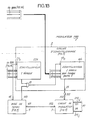
- a pulse modulator in duration MOD which according to a first embodiment, is intended to quantify and sample an incoming modulating analog analog signal SE and to convert words representing quantized values of the signal into durations impulse.
- the incoming modulating signal is, in general, an analog signal which can be an amplitude, frequency or phase modulation signal, such as for example a low frequency signal of the telephone signal type.
- the modulator MOD comprises a quantization circuit 1 for instantaneously quantifying the incoming voltage signal in IJ quantization intervals, a sampling circuit 2 for taking during a sampling period T e a quantization word transmitted by the circuit 2 and representative of a quantized value of the incoming signal, a modulation circuit 3 for converting each quantized value into a pulse duration modulating a carrier, and a time base 4 controlling circuits 2 and 3.
- a DEM demodulator receiving pulses of different durations transmitted by the modulation circuit 3 through an MV transmission means, for example such as a telephone line in a switched telephone network.
- the demodulator DEM includes a detection and validation circuit 5 for removing the carrier, detecting the pulses received and, preferably, for validating their duration, a demodulation circuit 6 for converting each detected pulse into a duration-dependent voltage sample of the detected pulse, and a time base 7.
- the quantization circuit 1 is an acyclic quantization circuit with high operating speed such as that described in French patent application 86-00305 filed on January 10, 1986 in the name of the current applicant. .
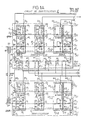
- Circuit 1 is divided into two quantizers QUA and qua by a differential input transformer TD.
- the incoming signal SE to be quantified is applied to a double primary winding EP + ep of the transformer TD and is reproduced and positively biased at the terminals of two secondary half-windings ES and es of the transformer.
- Each of the secondary half-windings ES, es has a terminal carried through a potentiometer PT, pt to a suitable positive voltage VMOY corresponding to an average value of the peak-to-peak amplitude of the incoming signal.
- the other terminals of the half-windings ES and es constitute input terminals BE, be of the quantizers QUA and qua respectively.
- Each of the cells C i of rows i between 1 and I-2 contains a detection circuit CD i for detecting an incoming voltage greater than a decision level defined by a lower limit voltage VT i and included in the respective quantization interval VT i to VT i + 1 , and a signaling circuit CS i for signaling by a logic state "1" to an output terminal BS i of the cell an incoming voltage included in this quantization interval.
- the first cell C0 only comprises a signaling circuit CS0 constituted by a simple inverter IN0, and the last cell C I-1 contains a detection circuit CD I-1 similar to those CD1 to CD I-2 in cells C1 to C I-2 , and a signaling circuit CS I-1 comprising only one diode D3 I-1 .
- the terminals of the resistors R21 and R2 I-1 are thus brought to the voltage limits VT0 to VT I quantization intervals.
- a terminal T i of the resistor R2 i connected to the resistor R2 i + 1 in the cell of rank i + 1 is brought to the voltage VT i , which is transferred through a diode D2 i to a terminal S i of a network of resistors and diodes in series.
- This latter network comprises between the input terminal BE and the anode of the diode D2 I-1 in the cell C I-1 , sets of diode and resistance in series D11, R11 to D1 I-1 , R1 I- 1 ; in a cell C i , the resistor R1 i is connected between emitters and base of a bipolar PNP transistor TR i .
- the diodes D11 to D1 i are conducting and the transistors TR1 to TR i are activated, or in other words, the transistor TR i is activated for a voltage at terminal BE exceeding the lower limit voltage VT i of the interval (VT i , VT i + 1 ) associated with cell C i , thanks to the voltage division created by the network of resistors R21 to R2 I-1 and the diode and resistance network R11 to R12 I-1 and D11 to D1 I-1 .
- the voltage at the BE terminal is adjusted to an average voltage substantially equal to VMOY and included in the quantization interval (VT I / 2-1 , VT I / 2 ) in particular when the quantification is uniform.
- the ohmic values of the resistances can be chosen to achieve a uniform quantization, or a non-uniform quantization deduced for example from a known logarithmic function of the curve type. compression of quantization levels for pulse code modulation of the MIC type.
- an AND gate P i has a first input connected to the collector of the transistor TR i in order to set to "1" an output terminal BS i of the cell C i only when the incoming voltage at the terminal BE is between VT i and VT i + 1 .
- the transistor TR i is blocked, which closes the gate P i .
- the output terminal of one of the cells C i + 1 to C I-1 is activated in state "1" which puts in state "0" a second input of the gate P i through a diode of the activated cell, equivalent to the diode D4 i in the cell C i , diodes in series between the activated cell and the cell C i , such as the diode D3 i in cell C i , and an inverter IN i in cell C i .
- a voltage of the polarized incoming signal between VT i and VT i + 1 is signaled by the state "1" at the output terminal BS i of the cell C i and by the state "0" at the output terminals BS0 to BS i-1 and BS i + 1 to BS I-1 of the other cells of the QUA quantizer.
- the second quantizer qua refines the quantization of the signal entering the first intervals (VT0, VT1) to (VT I-1 , VT I ) by dividing each of them into J second quantization intervals.
- the quantifier qua contains J second cells c0 to c J-1 arranged in a manner analogous to cells C0 to C I-1 .
- C0, c1 to c J-2 and c J-1 cells are respectively analogous to cells C0, C1 to C I-2 and C I-1 .
- components included in cell c j are designated by marks having lower case letters and numbers corresponding to capital letters and numbers of marks denoting equivalent components in cell C i .
- the cell numbers I and J in the quantifiers QUA and qua can be equal or different.
- the quantizer qua also includes first and second diode networks and resistors RDR1 and RDR2 for selectively applying the limit voltages of a first quantization interval when the corresponding output terminal of the first quantizer QUA is in the state "1".
- the first network RDR1 applies to the resistance r21 of the cell c1 the lower voltage of the first interval selected through a potentiometer ra1, while the second network RDR2 applies to the resistance r2 J-1 of cell c J-1 the upper limit of the first interval selected through a potentiometer ra2.
- a quantized value of the instantaneous voltage of the incoming signal is represented by a quantization word at a given instant composed of a first part having I-1 bits in the "0" state and a bit at l 'state “1" delivered in parallel by the outputs BS0 to BS I-1 and of a second part having J-1 bits in the state "0" and a bit in the state "1” delivered in parallel by the outputs bs0 to bs J-1 .
- the numbers I and J are assumed to be equal to 16 below, which corresponds to a quantization of the signal entering 256 quantization intervals.
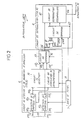
- the sampling circuit 2 thus operates a pulse modulation in position.
- the gates PE0 to PE I-1 have first inputs connected to the output terminals BS0 to BS I-1 of the first quantizer QUA, second inputs connected to the outputs of the I stages of the counter COM, and outputs connected to I input of an OR gate, respectively.
- the gate PO has an output connected to a first input 211 of an AND gate 21 having an output connected to a clock input eh0 of the counter com.
- the gates pe0 to pe J-1 have first inputs connected to the output terminals bs0 to bs J-1 of the second quantizer qua, second inputs connected to the outputs of the J stages of the counter com, and outputs connected to J entrances of a door OR po, respectively.
- the time base 4 includes a clock 41, a preferably programmable counter 42, a D type flip-flop 43, an AND gate with two inputs 44 and a frequency divider by J 45.
- the instant ⁇ 2 determines the start of transmission of an IM1 pulse ij by the modulation circuit 3.
- the IM1 pulse ij has a duration d1 ij which is a function of the ranks i and j of the bits BS i and bs j in the state "1" in the quantization word taken and less than or equal to d M , and therefore which is proportional to the instantaneous value of the incoming signal SE.
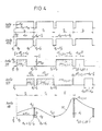
- the counter 42 and the flip-flop 43 in the time base 4 develop pulses of duration d M positioned in the periods T e as shown in a second line in FIG. 4.
- a clock input 42H of the counter 42 receives the clock signal h0 delivered by the clock 41.
- An output 421 of the counter 42 is connected to a clock input 43H of the flip-flop 43 and goes to " 1 "after a period d12 succeeding the start ⁇ 0 of a sampling period T e , as shown in the first line of FIG.
- an output 43Q of the latter then produces a pulse of duration d M from the instant ⁇ 2 of the period T e , pulse whose edge descending is obtained when an output 42M of the counter 42 sets a reset input 43R of the flip-flop 43 to "1", in response to a count of IJ clock pulses succeeding the instant ⁇ 2. Then after a count of clock pulses h0 for a period equal to d m , an output 42m of the counter 42 connected to a reset input 42R of the latter goes to "1" in order to reset the counter and outputs 421, 42M and 42m and establish a new sampling period.
- the duration d12 is equal to T e / 9, and the duration d m is equal to 0, the outputs 42M and 42m being combined, or is for example equal to T0, and is considered in the following as negligible compared to the durations d12 and d M , these being practically complementary in the period T e .
- the counter COM successively opens the doors PE0 to PE I-1 to read the I output terminals BS0 to BS I-1 of the quantizer QUA and thus detect the state "1" of one of these terminals, such as a terminal BS i , in response to the clock pulse of rank i + 1 applied to the input EH0 from time ⁇ 2.
- this pulse of rank i + 1 opens the gate 21 for a duration equal to JT0 succeeding a duration iJT0 from the instant ⁇ 2 in the sampling period T e in progress .
- a group of J consecutive clock pulses of period T0 is then applied to the clock input eh0 of the counter com by the output 213 of gate 21.
- the J clock pulses are counted in the counter com which opens successively the doors pe0 to pe N-1 to scan the J output terminals bs0 to bs J-1 of the quantizer qua and thus detect the state "1" of one of these terminals, such as a terminal bs j , in response to the clock pulse of rank j + 1 applied to the input eh0 during the duration JT0.
- the duration d12 + d1 ij - T0 determines the time position of the rising edge of the clock pulse leaving the door po in a period T e .
- the modulation circuit 3 comprises a flip-flop 30, an inverter 300, an AND gate with two inputs 31, an AND gate with three inputs 32, an inverter 33 and a generator 34 generating, preferably from the clock frequency 1 / T0, two carriers of frequency fp1 and fp2, preferably very close, by outputs 341 and 342.
- the flip-flop 30 has a setting input to "1" 30S connected to the output 421 of the counter 42, or at the input 442 of the door 42.
- a reset input to "0" 30R of the scale 30 is connected to the output 23 of the door OR po through the inverter 300.
- the rising front edge of such a pulse IM1 ij whatever i and j, is always positioned at time ⁇ 2 in a sampling period T e , as shown in a third line in Fig. 4.
- the modulation circuit 3 codes the first quantization level encountered in a pulse.
- the output 30Q of flip-flop 30 is reset to zero by the trailing edge falling from the clock pulse to terminal 23 and therefore immediately reset to zero after the pulse IM1 ij until the end of the sampling period .
- the modulation is therefore unequivocal between a pair of bits BS i and bs j in the state "1" and a pulse IM1 ij .
- the pulse IM1 ij obtained at output 30Q opens the door 31 having inputs connected to terminals 30Q and 341.
- An output 311 of the AND gate 31 transmits the pulse IM1 ij modulating the carrier frequency fp1 for the duration d1 ij .
- an output 321 of the AND gate 32 delivers a pulse IM2 ij modulating the carrier frequency fp2 and having a duration d2 ij equal to the complement of the duration d1 ij during the duration d M of the sampling period, or more generally during the duration d M + d m , i.e.
- the pulse IM2 ij always having a falling edge positioned at the end d 'a period T e , as shown in a fourth line in Fig. 4.
- the three inputs of gate 32 are respectively connected to output 421 of counter 42 in the time base, to output 30Q of flip-flop 30 through inverter 33, and to output 342 of generator 34.
- the transmission means MT conveys the frequency multiplexed IM1 ij and IM2 ij pulses in two parallel lines.
- the reception of the pairs of successive pulses IM1 ij and IM2 ij makes it possible to test the conformity of the received signal by checking that the sum of the durations of two "complementary" pulses is always constant and equal to d M , or d M + d m , during each sampling period T e .
- the modulator only comprises a quantizer QUA and a sampler ECH when the number of quantization levels is small; in this case, the output of the OR gate PO (Fig.3) is directly connected to the input 30R of the rocker 30 through the inverter 300.
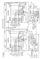
- the DEM demodulator is now described with reference to Figs. 2, 5 and 6.
- pulses IM1 ij and IM2 ij modulating the carrier frequencies fp1 and fp2 are respectively received at inputs 5011 and 5012 from two carrier detectors 501 and 502 included in the circuit pulse detection and validation 5 shown in Fig. 5.
- the detectors 501 and 502 are preferably pulse detection devices according to their duration of the kind described in French patent application 85-15418 filed on October 17, 1985, in the name of the current applicant.
- detectors 501 and 502 are programmed by the time base 7 to detect alternating sinusoids of widths 1 / (2fp1) and 1 / (2fp2) and thus restore continuous voltages in response to the carriers fp1 and fp2 during the durations d1 ij and d2 ij of the pulses IM1 ij and IM2 ij respectively.
- Outputs 5021 and 5022 thus restore two pulses IM1 ij and IM2 ij without carrier, in each sampling period T e .
- the circuit 5 also includes a complementarity checking circuit 51, a complementary pulse selection circuit 52 and a control circuit 53 at the output.
- the complementarity verification circuit 51 comprises an OR-Exclusive gate 511 having two inputs respectively connected to terminals 5021 and 5022, a pulse detection device 512 connected to the output of gate 511, an AND gate 513 having a first input directly connected to output 514 of device 512 and a second input connected to output 5021 through a delay line 5211, and an inverter 515 connected to output 514 of device 512.
- an OR-Exclusive gate 511 having two inputs respectively connected to terminals 5021 and 5022, a pulse detection device 512 connected to the output of gate 511, an AND gate 513 having a first input directly connected to output 514 of device 512 and a second input connected to output 5021 through a delay line 5211, and an inverter 515 connected to output 514 of device 512.
- Device 512 is of the kind described in the aforementioned patent application 85-15418, and is programmed by the time base 7 to detect pulses of width d M , or d M + d m , at period T e , it is i.e. to detect pulses periodicals of width d M , or d M + d m , spaced by a time difference equal to d12.
- the output 514 of the device 512 is in the state "1" as long as pulses at the output of the gate 511 have widths of d M , or d M + d m , and time differences between them of d12, c ' that is, as long as pulses IM1 ij and IM2 ij are strictly complementary during the duration d M , or d M + d m , in the periods T e .
- the AND gate 513 is open to transmit the pulses IM1 ij applied by the delay line 5211 to an input 532 C of an OR gate with three inputs 531 included in the control circuit 53.
- the pulses IM2 ij are transmitted by the gate 513 by connecting the input of the delay line 5211 to the output 5022 of the detector 502, or by connecting the second input of gate 513 only to output 5022 through a delay line 5212.
- the delay line 5211 like the other delay line 5212 in the selection circuit 52, imposes a delay equal to d M or d M + d m , or equal to 2d M + T e or 2 (d M + d m ) + T e according to the type chosen of the device 512 in order to compensate for the delay imposed by the detection of pulses of duration d M , or d M + d m in the device 512.
- d M is equal to 0, or that d M can be replaced by d M + d m .
- the gate 513 is closed and an output of the inverter 515 activates an AND gate with three inputs 523 and an AND gate with two inputs 524 included in the selection circuit 52. Two conditions are then to be distinguished in the absence of pulse complementarity.
- the absence of complementarity is due to an lengthening or a shortening of the duration of one of the detected pulses IM1 ij and IM2 ij .
- the received signal is then eliminated by closing the AND gate 524 thanks to two monostable flip-flops 5251 and 5252 interconnected respectively between the terminals 5011 and 5012 and two other inputs of the AND gate 523 having an output connected to a second input of the gate 524 through an inverter 526.
- the monostable flip-flops have time constants equal to T e and are retriggerable by the rising front edges of the pulses IM1 ij and IM2 ij respectively, so that in the presence of successive and non-consecutive pulses IM1 ij and IM2 ij , door 523 is open and closes door 524 which in turn closes two AND doors with two inputs 5271 and 5272.
- the AND gates 5271 and 5272 receive by second inputs the pulses IM1 ij and IM2 ij through the delay lines 5211 and 5212 and have outputs connected to the two other inputs 5321 and 5322 of OR gate 531, respectively.
- the output of gate 523 in state "1" can command the sending back, to the transmission part comprising the modulator, of a signal requesting the repetition of part of the message, such as last character or byte transmitted.
- the complementarity is not observed by the Exclusive-OR gate 511 and the device 512, and one of the pulses IM1 ij and IM2 ij is not detected by the detectors 501 and 502.
- one of the monostable flip-flops 5251 and 5252 is not triggered which closes the door 523 and opens the door 524 which controls the passage of the detected pulse IM1 ij or IM2 ij through the respective open AND gate 5271 or 5272.
- the demodulation of the pulses IM1 ij and that of the pulses IM2 ij lead to signals in phase opposition which, in the general case and insofar as the disturbance is weak, has no effect on a phonic or digital restitution of the demodulated signal.
- the control circuit 53 comprises, in addition to the OR gate 531, two doors 533 and 534 respectively having first inputs connected to the terminal 5021 through the delay line 5211, and at the output of the OR gate 531, second connected inputs through an inverter 535 and directly to a control terminal 5C, and outputs connected to an input terminal 6E of the demodulation circuit 6 through an OR gate with two inputs 536.
- the control terminal 5C in the "1" state activates the circuits 51 and 52 of the detection and validation circuit 5 by opening the door 534 and closing the door 533 in order to transmit through the door OR 531 of the first IM1 ij pulses validated by the device 512 or of the pulses selected from among IM1 ij and IM2 ij pulses detected by the circuit 52.
- terminal 5C is at state "0"
- door 534 is closed and p orte 533 is open to transmit directly uncontrolled pulses IM1 ij without carrier delivered by the terminal 5021 through the delay line 5211.
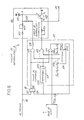
- the demodulation circuit 6 comprises a flip-flop 61 for detecting the rising edges of the pulses IM1 ij , to which reference is made below, or possibly of the pulses IM2 ij , received at the input 6E, a circuit for reproducing samples of the incoming signal 62, and a control circuit 63 for taking samples.
- the sample reproducing circuit 62 essentially comprises a capacitor 621 which, during each sampling period, is charged by a voltage depending on the width of a pulse IM1 ij received during this period, then is completely discharged, and an element with variable resistivity in the form of a field effect transistor with high input impedance of the unijunction transistor type 622 which is supplied by the voltage memorized by the capacitor 621 and therefore proportional to the duration d1 ij of the pulse received IM1 ij and at the corresponding quantized voltage level of the incoming signal SE and established in the quantization circuit 1.
- the capacitor 621 has an armature brought to earth and another armature A which is connected to the emitter E of conductivity P of transistor 622 , to the cathode of a diode 623 through an adjustable resistor 624, and to the anode of a diode 625.
- the anode of diode 623 is connected to the input terminal 6E and to a switching terminal "1 "61S of flip-flop 61.
- Bases B1 and B2 of transistor 622 are respectively connected to earth and to an output terminal 6S of the demodulation circuit connected to an adjustable resistance terminal 626.
- the control circuit 63 comprises three AND gates with two inputs 631, 632 and 633, a counter 634 and a monostable latch triggerable by falling edge 635. First inputs of the gates 631, 632 and 633 are connected to an output 61Q of the latch bistable 61 so that these three doors are activated in response to a rising edge of a pulse IM1 ij detected at input 6E by flip-flop 61.
- Such a clock signal can be obtained from a clock supplying a clock signal of period T0 from which the time base 7 also establishes, by means of programmable frequency dividers, clock frequencies necessary for the pulse detection devices 501 , 502 and 512 in the detection and validation circuit 5.
- the time base 7 is completely independent of the time base 4 in the MOD modulator and, consequently, the modulation and demodulation operations are asynchronous and do not require a any clock recovery circuit in the DEM demodulator thanks to the 501, 502 and 512 devices.
- the counter 634 here comprises five stages and receives at a clock input 634H the clock signal of period d1 through the gate 631.
- a first output 634 M of the counter 634 is connected to a second input of the gate 632 having a output connected through the resistor 626 to the terminal 6S and therefore to the control base B2 of the transistor 622.
- a second output 6341 of the counter 634 is connected on the one hand to a second input of the gate 633 having an output connected to the cathode of diode 625 through an inverter 636, on the other hand to an input 635S of the monostable flip-flop 635 having an output 635Q connected to reset inputs 61R and 634R of flip-flop 61 and of the counter 634.
- the outputs 634 M and 6341 remain in the "0" state until the counter 634 has counted down a duration d M.
- the gate 632 is blocked and provides an earth output to block the unijunction transistor 622 and thus keep a zero voltage at terminal 6S.
- the gate 633 is blocked and its output is at "0" which blocks the diode 625 through the inverter 636 and allows charging of the capacitor 621 through the diode 623 and the resistor 624.
- the resistor 624 is adjusted beforehand so that the charge curve of the capacitor 621 for a duration equal to or less than d M is substantially a straight line. Under these conditions, the capacitor 621 is charged for the duration d1 ij of the pulse IM1 ij which is normally less than or equal to d M.
- the output 634 M of the counter goes to "1" which opens the gate 632 and turns on the transistor 622 for a duration d1 succeeding d M , the door 633 being still closed.
- this duration d1 that is to say between instants M and ⁇ M + d1 of a sampling period T e as shown in a fifth line of FIG. 4, the charge voltage of the capacitor 621 is applied to the transistor 622 and determines the conductivity of the latter so that the output terminal 6S of the demodulation circuit delivers a sample whose amplitude is a linear function of the duration d1 ij of the pulse IM1 ij .
- terminal 6S collects analog samples e ij of duration d1 having amplitudes proportional to the durations es d1 ij of the pulses IM1 ij and therefore to the corresponding quantization levels.
- the output 634 M goes to "0" which closes the gate 632, blocks the transistor 622 and puts the terminal 6S at the potential of 0 volts, and the output 6341 goes to "1" for a time d2 to open the door 633 and completely discharge the capacitor 621 through the pass-through diode 625.
- the samples e ij of duration d1 at terminal 6S are then amplified and smoothed in known means to restore the analog signal SE initially entering the modulator MOD.
- the quantization circuit 1 can be used to convert N analog signals SE1 to SE N into pulses modulated in duration.
- the time base 4 produces addressing signals to switching circuits to successively select samples of the N analog signals during a cycle of duration NT e which are quantized in circuit 1 and converted into pulses modulated in duration. by the sampling circuit 2 and the flip-flop 30.
- the output 30Q of the flip-flop is connected to N pairs of AND gates 311, 321 to 31 N , 32 N , such as gates 31 and 32, which are successively opened by the addressing signals.
- the AND gate pairs 311, 321 to 31 N , 32 N respectively receive pairs of different carriers f p 11, f p 21 to f p1N , f p2N .
- the lowest carrier frequencies are substantially greater than the frequency of the clock signal h0.
- N demodulators according to the invention demodulate the pulses modulating the carrier frequencies into the signals SE1 to SE N respectively.
- This multiple modulation allows for example a direct injection into a subscriber telephone line, of pulses modulated in duration through a subscriber line signaling equipment for telephone switch, as described in the French patent application FR-A -2 585 526 in the name of the current applicant; the signals injected in the form of pulses relate in particular to telephone signaling, artificial speech and telephone modulation proper.
- the incoming signal is a digital signal, such as a 2048 kbit / s MIC signal conveying thirty-two channels.
- Each of the multiplexed channels has a byte occupying a time window of 3.9 ⁇ s in a frame of 125 ⁇ s.
- the transcoding circuit can include memories or counters.
- a conventional clock signal recovery circuit at a frequency of 2048 kHz and a frame frequency of 8 kHz makes it possible to control the transcoding circuit and to supply the frequency 1 / T0 to the time base 4.
- the MIC system can be used with an asynchronous time multiplexing making the frame locking channel unnecessary. It then takes 3 time modulation devices to process a set of 30 MIC channels on the basis of counters operating at 25 MHz.
- the bits "1" and “0" are respectively coded in pulses of respective durations d11, d21 and d10, d20 such that d11> d10 and d21 ⁇ d20.
Landscapes
- Engineering & Computer Science (AREA)
- Theoretical Computer Science (AREA)
- Dc Digital Transmission (AREA)
- Compression, Expansion, Code Conversion, And Decoders (AREA)
- Analogue/Digital Conversion (AREA)
Applications Claiming Priority (2)
| Application Number | Priority Date | Filing Date | Title |
|---|---|---|---|
| FR8600357 | 1986-01-13 | ||
| FR8600357A FR2593006A1 (fr) | 1986-01-13 | 1986-01-13 | Modulateur et demodulateur d'impulsions modulees en duree |
Publications (2)
| Publication Number | Publication Date |
|---|---|
| EP0230838A2 true EP0230838A2 (de) | 1987-08-05 |
| EP0230838A3 EP0230838A3 (de) | 1988-04-13 |
Family
ID=9331032
Family Applications (1)
| Application Number | Title | Priority Date | Filing Date |
|---|---|---|---|
| EP86402963A Withdrawn EP0230838A3 (de) | 1986-01-13 | 1986-12-30 | Pulsbreitenmodulator und -demodulator |
Country Status (2)
| Country | Link |
|---|---|
| EP (1) | EP0230838A3 (de) |
| FR (1) | FR2593006A1 (de) |
Family Cites Families (6)
| Publication number | Priority date | Publication date | Assignee | Title |
|---|---|---|---|---|
| FR1587806A (de) * | 1968-10-03 | 1970-03-27 | ||
| BE791513A (fr) * | 1971-11-19 | 1973-03-16 | Northern Illinois Gas Co | Convertisseur analogique-numerique a couplage electrostatique |
| JPS5438844B2 (de) * | 1974-07-19 | 1979-11-24 | ||
| JPS5227302A (en) * | 1975-08-27 | 1977-03-01 | Sony Corp | Station selecting device |
| JPS56152373A (en) * | 1980-04-24 | 1981-11-25 | Fuji Photo Film Co Ltd | Laser recording device |
| FR2558316B1 (fr) * | 1984-01-12 | 1989-10-20 | Pophillat Lucien | Procede de modulation synchrone d'un signal analogique, modulateur et demodulateur pour la transmission d'un signal suivant ce procede et procede de transmission de signaux numeriques et analogiques en trame appliquant |
-
1986
- 1986-01-13 FR FR8600357A patent/FR2593006A1/fr not_active Withdrawn
- 1986-12-30 EP EP86402963A patent/EP0230838A3/de not_active Withdrawn
Also Published As
| Publication number | Publication date |
|---|---|
| FR2593006A1 (fr) | 1987-07-17 |
| EP0230838A3 (de) | 1988-04-13 |
Similar Documents
| Publication | Publication Date | Title |
|---|---|---|
| EP0194902B1 (de) | Verfahren und Einrichtung zur Spreizbandübertragung, insbesondere zur Informationsübertragung auf ein elektrisches Energieverteilungsnetz | |
| CA1173965A (fr) | Procede et dispositif de detection de la sequence d'apprentissage d'un egaliseur autoadaptatif | |
| EP0013343B1 (de) | Verfahren und Vorrichtung zur Auffindung einer Pseudo-Zufallsfolge von 0 Grad- und 180 Grad-Phasenänderungen der Trägerwelle in einem Datenempfänger | |
| FR2652215A1 (fr) | Procede de codage d'un signal numerique, codeur et decodeur pour la mise en óoeuvre de ce procede, procede de regeneration et regenerateur correspondant. | |
| CH624250A5 (de) | ||
| CH685460A5 (fr) | Procédé de commande du balayage des canaux d'appel par un poste mobile d'un système de radio-téléphone à cellules. | |
| FR2511170A1 (fr) | Systeme de poursuite de seuil automatique | |
| FR2674390A1 (fr) | Dispositif de transmission d'informations numeriques sur une ligne d'un reseau d'energie electrique. | |
| FR2498032A1 (fr) | Synchroniseur de bits pour signaux numeriques | |
| FR2467523A1 (fr) | Systeme de controle d'un reseau de connexion | |
| FR2583883A1 (fr) | Dispositif et procede pour produire un facteur de merite de rapport signal a bruit pour des donnees en codage numerique | |
| FR2693062A1 (fr) | Procédé et dispositif égaliseur à retour de décisions pour la transmission par blocs de symboles d'information. | |
| EP0012884B1 (de) | Verfahren und Vorrichtung zur Auffindung einer Pseudo-Zufallsfolge zweier Symbole in einem Datenempfänger, welcher eine Doppelzeitenbandmodulation mit Quadraturträgern verwendet | |
| FR2818784A1 (fr) | Recepteur radiofrequence pour la telereleve de compteurs et methode de telereleve de compteurs comprenant un tel recepteur | |
| FR2687876A1 (fr) | Ensemble de detection d'erreurs pour ligne de transmission numerique et procede de surveillance. | |
| EP0090728A1 (de) | Verfahren zur gemeinsamen Übertragung eines Signals im HDBN-Kode und eines binären Hilfssignals, Kodierer und Dekodierer nach diesem Verfahren und System zur Fernüberwachung von Zwischenverstärkern einer Digitalverbindung mit Hilfe solcher Hilfssignale | |
| EP0097579A1 (de) | Funkverbindungssystem nach dem Frequenzsprungverfahren mit Redundanz zwischen den einzelnen Frequenzstufen | |
| EP0018256B1 (de) | Sender-Empfänger mit automatischer Steuerung der Sende-Empfangsumschaltung und Fernmeldenetz, welches einen solchen Sender-Empfänger enthält | |
| EP0515277B1 (de) | Modulare Beobachtungsanordnung zur Verkehrsbeobachtung von digitalen Signalen | |
| EP0230838A2 (de) | Pulsbreitenmodulator und -demodulator | |
| EP0384536B1 (de) | Verfahren und Anordnung für die Bitsynchronisation in einem digitalen Datenempfänger | |
| FR2538590A1 (fr) | Appareil de reproduction de signal numerique | |
| FR2574201A1 (fr) | Procede et dispositif de telesignalisation pour une liaison de transmission numerique | |
| EP1202513A1 (de) | Universaler Modem | |
| CA2082288C (fr) | Methode et dispositif pour restituer un signal d'horloge rythmant la transmission de signaux recus |
Legal Events
| Date | Code | Title | Description |
|---|---|---|---|
| PUAI | Public reference made under article 153(3) epc to a published international application that has entered the european phase |
Free format text: ORIGINAL CODE: 0009012 |
|
| 17P | Request for examination filed |
Effective date: 19870325 |
|
| AK | Designated contracting states |
Kind code of ref document: A2 Designated state(s): BE CH DE GB LI NL |
|
| PUAL | Search report despatched |
Free format text: ORIGINAL CODE: 0009013 |
|
| AK | Designated contracting states |
Kind code of ref document: A3 Designated state(s): BE CH DE GB LI NL |
|
| STAA | Information on the status of an ep patent application or granted ep patent |
Free format text: STATUS: THE APPLICATION IS DEEMED TO BE WITHDRAWN |
|
| 18D | Application deemed to be withdrawn |
Effective date: 19880614 |