EP0227464B1 - Hochdichter Festwertspeicher - Google Patents
Hochdichter Festwertspeicher Download PDFInfo
- Publication number
- EP0227464B1 EP0227464B1 EP86310023A EP86310023A EP0227464B1 EP 0227464 B1 EP0227464 B1 EP 0227464B1 EP 86310023 A EP86310023 A EP 86310023A EP 86310023 A EP86310023 A EP 86310023A EP 0227464 B1 EP0227464 B1 EP 0227464B1
- Authority
- EP
- European Patent Office
- Prior art keywords
- lines
- row
- select
- address
- terminals
- Prior art date
- Legal status (The legal status is an assumption and is not a legal conclusion. Google has not performed a legal analysis and makes no representation as to the accuracy of the status listed.)
- Expired - Lifetime
Links
- 230000015654 memory Effects 0.000 title claims description 92
- 230000008878 coupling Effects 0.000 claims description 17
- 238000010168 coupling process Methods 0.000 claims description 17
- 238000005859 coupling reaction Methods 0.000 claims description 17
- 230000005669 field effect Effects 0.000 claims description 2
- VYPSYNLAJGMNEJ-UHFFFAOYSA-N Silicium dioxide Chemical compound O=[Si]=O VYPSYNLAJGMNEJ-UHFFFAOYSA-N 0.000 description 6
- 239000004020 conductor Substances 0.000 description 5
- 238000010586 diagram Methods 0.000 description 5
- 238000001465 metallisation Methods 0.000 description 5
- 229910021420 polycrystalline silicon Inorganic materials 0.000 description 4
- 239000004065 semiconductor Substances 0.000 description 4
- 229920005591 polysilicon Polymers 0.000 description 3
- 235000012239 silicon dioxide Nutrition 0.000 description 3
- 239000000377 silicon dioxide Substances 0.000 description 3
- 238000004519 manufacturing process Methods 0.000 description 2
- 230000004044 response Effects 0.000 description 2
- XUIMIQQOPSSXEZ-UHFFFAOYSA-N Silicon Chemical compound [Si] XUIMIQQOPSSXEZ-UHFFFAOYSA-N 0.000 description 1
- 238000007796 conventional method Methods 0.000 description 1
- 238000012937 correction Methods 0.000 description 1
- 230000001934 delay Effects 0.000 description 1
- 238000013461 design Methods 0.000 description 1
- 230000000694 effects Effects 0.000 description 1
- 238000002513 implantation Methods 0.000 description 1
- 230000002401 inhibitory effect Effects 0.000 description 1
- 239000011159 matrix material Substances 0.000 description 1
- 239000002184 metal Substances 0.000 description 1
- 229910044991 metal oxide Inorganic materials 0.000 description 1
- 150000004706 metal oxides Chemical class 0.000 description 1
- 229910052710 silicon Inorganic materials 0.000 description 1
- 239000010703 silicon Substances 0.000 description 1
- 239000000758 substrate Substances 0.000 description 1
- 238000012546 transfer Methods 0.000 description 1
Images

Classifications
-
- G—PHYSICS
- G11—INFORMATION STORAGE
- G11C—STATIC STORES
- G11C17/00—Read-only memories programmable only once; Semi-permanent stores, e.g. manually-replaceable information cards
- G11C17/08—Read-only memories programmable only once; Semi-permanent stores, e.g. manually-replaceable information cards using semiconductor devices, e.g. bipolar elements
- G11C17/10—Read-only memories programmable only once; Semi-permanent stores, e.g. manually-replaceable information cards using semiconductor devices, e.g. bipolar elements in which contents are determined during manufacturing by a predetermined arrangement of coupling elements, e.g. mask-programmable ROM
- G11C17/12—Read-only memories programmable only once; Semi-permanent stores, e.g. manually-replaceable information cards using semiconductor devices, e.g. bipolar elements in which contents are determined during manufacturing by a predetermined arrangement of coupling elements, e.g. mask-programmable ROM using field-effect devices
- G11C17/126—Virtual ground arrays
Definitions
- This invention relates generally to integrated circuit memories, and more particularly, to read-only integrated circuit memories (ROMS).
- ROMS read-only integrated circuit memories
- the bit lines carry data from the memory cells to sense amplifiers.
- Memory cells are arranged in an array NxM in regions bounded by the two sets of column lines and the set of row lines. Each memory cell is coupled to an adjacent column line, an adjacent bit line, and an adjacent row line. Memory cells are selected by enabling one column line and one row line. Therefore, each row address conductor has M memory cells coupled thereto and each column line has 2N memory cells coupled thereto.
- one of the row lines is enabled and one of the two groups of column lines is enabled. This causes those memory cells coupled to the enabled row line and to the enabled column lines to transfer their stored information to their respective bit lines.
- Each column line is heavily loaded capacitively because of the 2N memory cells coupling to it.
- a nonvolatile integrated circuit memory comprising: (a) a plurality of select lines extending in a row direction and a plurality of bit lines extending in a column direction forming rows and columns of regions, each region having four memory cells with a common enable terminal, four independent output terminals, and independent address terminals interposed between the common enable terminal and each of the corresponding independent output terminals, whereby the independent address terminals form two rows of two independent address terminals in each region; (b) the plurality of bit lines coupling to respective columns of the independent output terminals, in such a manner that in each region a first two of the four independent output terminals couple to one adjacent bit line and a second, different two of the four independent output terminals couple to a different, adjacent bit line; (c) the plurality of select lines extending in the row direction coupling to the common enable terminals in the regions; and (d) a plurality of row lines coupling to respective rows of independent address terminals in the formed regions, and the arrangement being such that
- a nonvolatile integrated circuit memory having an address and virtual ground decoder coupling to a plurality of row lines and a plurality of select lines, each one of the plurality of row lines and corresponding ones of the plurality of select lines being coupled to a corresponding row of paired memory cells for selecting one memory cell in each of the pair of memory cells in a corresponding row of paired memory cells
- the decoder comprising: a plurality of input address lines; a pair of input address lines; a decoder means, coupled to the plurality of input address lines, for enabling one of a plurality of outputs; a first selecting means, responsive to the decoder means and a first one of the pair of input address lines, for enabling a selected one of the plurality of row lines; and a second selecting means, responsive to the plurality of outputs of the decoder means, and a second one of the pair of input address lines, for enabling a selected one of the plurality of select lines that corresponds to the selected
- a preferred embodiment of this invention provides a high density memory with a structure that has reduced loading on the column lines to allow smaller, lower power drivers for the column lines, and that allows a common decoder circuitry for both column and row lines, the decoder using common circuitry to drive the column and row drivers.
- select lines are arranged such that they correspond and are parallel to the row lines. Additionally, the select lines are independent of each other.
- NXM memory array there are N row lines, N/2 select lines, each row address line couples to M memory cells and each select address line couples to M memory cells (instead of the 2N memory cells per column line in the prior art).
- each select line has half the capacitive loading a column line in the prior art has.
- a row line is enabled and only those select lines corresponding to the enabled row line (typically one or two) are enabled instead of half of the column lines as in the prior art.
- each select line being lightly loaded and with only one or two of corresponding select lines enabled, less electrical noise is generated and less power is dissipated during a read of the memory compared to the prior art.
- the smaller loading on the select lines allows smaller, less powerful drivers to drive these select lines compared to the column line drivers needed in the prior art.
- decoders for the select lines can share decoding logic with the row decoders. These features allow more area to be available for memory cells.
- An address and select line decoder is provided which uses multiple stages of decoders to decode an input address.
- Decoding of the input address has several common stages of decoding, allowing an efficient scheme to enable one row line and have only those select lines enabled that correspond to that enabled row line. By enabling only those select lines that correspond to an enabled row line, power dissipation, electrical noise generation and access time of the memory is reduced. Additionally, common decoder circuitry allows more chip area available for memory cells.
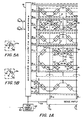
- a semiconductor integrated circuit memory (ROM) 10 is shown to include: an array 12 of memory cells 14, arranged in pairs 17.
- the memory cells 14 are arranged in a matrix of 2 m rows 71 and n columns (not numbered), as shown, storing 2 m by n bit digital words, where m is the number of bits used to address the ROM 10.
- Corresponding with each row 71 are a pair of 2 m-1 select lines SL0 ⁇ -SL (2 m -1) ⁇ .
- One of the pair of corresponding select lines SL0 ⁇ -SL (2 m-1 ) ⁇ is connected to a first one of the memory cells 14 in each pair 17 and the second one of the pair of corresponding select lines SL0 ⁇ -SL (2 m -1) ⁇ is connected to the other one of the memory cells 14 in the pair 17. It is next noted that a pair of adjacent row lines RL0-RL (2 m-1 ) is disposed between successive select lines SL0 ⁇ -SL (2 m-1 ) ⁇ and each row line RL0-RL (2 m-1 ) couples to each memory cell 14 in corresponding rows 71.
- the memory 10 also includes: an address and select line decoder 16; a sense amplifier section 18; and a ROM enable circuit 62.
- decoder 16 enables, or addresses, one of 2 m row conductors (i.e., row lines RL0-RL (2 m -1) , as shown, selectively in accordance with address signals on lines A0-A m-1 . More particularly, decoder 16 drives all but one of the row lines RL0-RL (2 m -1) “low” (to ground) while driving the enabled or addressed row line RL0-RL (2 m -1) “high” (+V DD ).
- the address and select line decoder 16 enables, or addresses, a selected two of the select SL0 ⁇ -SL (2 m -1) ⁇ , corresponding to the enabled row line RL0-RL (2 m -1) during a read of the ROM.
- Column conductors, or bit lines BL0-BL (n-1) carry the binary data accessed in addressed memory cells 14 to the sense amplifier section 18 to thereby read from the memory cell array 12 the n-bits of the addressed one of the 2 m+1 n-bit digital words stored in such ROM 10; such digital words having been masked programmed into the ROM 10 during its fabrication as an integrated circuit.
- the sense amplifiers in the sense amplifier section 18 are of a conventional design, each one thereof being coupled to a corresponding one of the bit lines BL0-BL (n-1) to produce at the output of such sense amplifier section 18 an n-bit digital word O0-O (n-1) .
- the sense amplifier section 18 and address and select line decoder 16 are controlled by the ROM enable circuitry 62 by the enable signal on line 64.
- An external input chip enable signal fed to input 60 controls ROM enable circuitry 62 by enabling ROM enable circuitry 62 when a ROM read cycle is requested (input 60 is "high”) and disabling it when in the standby mode (input 60 is "low”).
- each memory cell 14 in that pair 17 has an output terminal 32, enable terminal 30 and an address terminal 31 disposed between the enable terminal 30 and the output terminal 32.
- the output terminals 32 in the memory cell pair 17 are coupled to a common output terminal 24, which is in turn coupled to a corresponding bit line BL0-BL (2 n-1 ) .
- the address terminals 31 of all the memory cells 14 in the memory cell row 71 are coupled to a corresponding one of the row lines RL0-RL (2 m -1) .
- the select lines SL0 ⁇ -SL (2 m -1) ⁇ are disposed adjacent to alternating memory cell rows 71.
- the enable terminal 30 of a first one of the memory cells 14 in each memory cell pair 17 couples to a first one of the adjacent select lines SL0 ⁇ -SL (2 m -1) ⁇ and the enable terminal 30 of the second one of the memory cells 14 of the pair 17 couples to a different one of the adjacent select lines SL0 ⁇ -SL (2 m -1) ⁇ . Because each memory cell 14 of each memory cell pair 17 is coupled to a different one of the select lines SL0 ⁇ -SL (2 m-1 ) , when the corresponding row line RL0-RL (2 m-1 ) is enabled, the binary data stored in one of the memory cells 14 is passed to the common output terminal 24. Therefore, two memory cells 14 coupled to a common output terminal 24 cannot be enabled simultaneously.
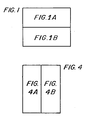
- each memory cell 14 (FIGS. 1A, 1B) is an n-channel enhancement mode metal oxide semiconductor (MOS) field effect transistor (FET).
- MOS metal oxide semiconductor
- the output terminal 32 couples to the drain D
- the enable terminal 30 couples to the source S
- the address terminal 31 couples to the gate G of the FET.
- Each one of the cells 14 (FIGS. 1A, 1B) is programmed to have transistor action (to store a logic 0), as shown in FIG. 5A, or is programmed not to have transistor action (to store a logic 1) as shown in FIG. 5B.
- Transistor action occurs where signals on the address terminal 31 can control the conductivity between the drain D and the source S (FIG. 5A).
- Transistor action is inhibited where signals on the address terminal 31 cannot control the conductivity (FIG. 5B).
- transistor action is inhibited, a high impedance state exists between the source S and drain D.
- cell 14a is enabled, a low impedance state exists between the drain D and the source S.
- the ROM enable circuitry 62 controls the ROM 10 in a pre-charge state by placing a disable signal on line 64.
- address and select line decoder 16 is disabled so that all the row lines RL0-RL (2 m -1) are "low” (ground) and all the select lines SL0 ⁇ -SL (2 m -1) ⁇ are "high” (+V DD ).
- the disable signal on line 64 disables the sense amplifiers in the sense amplifier section 18 to pre-charge the bit lines BL0-BL (n-1) to +V DD .
- the ROM enable circuit 62 sends an enable signal on line 64, releasing the address and select line decoder 16 and the sense amplifiers in sense amplifier section 18 to access the desired memory cells 14.
- Operation of the ROM 10 during a read cycle while referring specifically, by way of example, to enable signals on row line RL1, select lines SL 0,1 and SL 2,3 , and an exemplary pair of memory cells 17a connected to bit line BL1, it is first noted that an enable signal on row line RL1 (a "high”) and select line SL 2,3 (a “low”) places the memory cell 14a′′′ into a conduction condition (having been programmed with transistor action), to discharge the stored charge over bit line BL1 from +V DD toward ground.
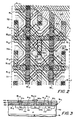
- FIG. 3 is a cross-sectional view along the 3-3 line in FIG. 2. It is additionally noted that each one of the memory cells 14 is formed in different regions of the semiconductor body used to fabricate the ROM 10 as an integrated circuit. During fabrication of the ROM 10 as an integrated circuit, those memory cells which are to store a logic 0 data bit have formed in that element an FET having transistor action, designated here as 14a (FIG. 5A). A memory cell 14 that is to store a logical 1 has its transistor action inhibited as 14b (FIG. 5B).
- N+type conductivity regions 33a and 34a, 34c, forming the source S and drain D of cells 14a, 14b are diffused into a grounded p-type conductivity ground well 40.
- This well 40 is electrically coupled to ground through a ground bus (not shown).
- This well 40 is disposed in an n-type conductivity silicon substrate 41.
- the row lines RL0-RL (2 m -1) consist of doped polycrystalline silicon (polysilicon), with portions thereof providing gate electrodes G (FIGS. 5A, 5B). Further, as described above, the gate electrode G (FIG.
- memory element 14a is disposed over a thin silicon dioxide insulating layer 42 in etched area 50 (FIG. 3) of silicon dioxide on the portions of the surface of the well 40 between the regions 33a and 34a to provide an n-channel enhancement mode FET.
- a thick portion of silicon dioxide insulating layer 42 is formed between the regions 33a, 34c to destroy any gate channel between such regions 33a, 34c and thus inhibit transistor action between regions 33a, 34c. It is here noted that while the use of a thick oxide layer between the source and drain regions to prevent transistor action has been described, other conventional techniques can be used to prevent such transistor action, such as active area removal or implantation into the channel region to raise the transistor threshold for conducting current.
- the bit lines BL0-BL (n-1) are formed by a first level of metallization insulated from the polysilicon row lines RL0-RL (2 m -1) by oxide layer 43, and are arranged perpendicularly to the row lines RL0-RL (2 m -1) .
- the select lines SL0 ⁇ -SL (2 m -1) ⁇ are formed by a second level of metallization insulated from the bit lines BL0-BL (n-1) by oxide layer 44, and are arranged to parallel the row lines RL0-RL (2 m -1) .
- These select lines SL0 ⁇ -SL (2 m-1 ) ⁇ are coupled to corresponding n+type conductivity regions 33 via contacts 36, such regions being diffused within well 40.
- the second level of metallization first couples to a first level of metallization which, in turn, couples to the n+ type conductivity region instead of directly going from a second level of metallization to the n+ type conductivity region as shown.
- first level of metallization which, in turn, couples to the n+ type conductivity region instead of directly going from a second level of metallization to the n+ type conductivity region as shown.
- second level metal couples to a first level of metallization which, in turn, couples to the n+ type conductivity region instead of directly going from a second level of metallization to the n+ type conductivity region as shown.
- the bit lines BL0-BL (n-1) are coupled thereto via contacts 37, such regions being diffused within well 40.
- the select lines SL0 ⁇ , SL (2 m -1) ⁇ are arranged in rows such that they cross the semiconductor bulk comprising the ROM array over where the bit lines BL0-BL (n-1) couple to the n+ region contacts 37.
- the columns of bit lines BL0-BL (n-1) and the rows of select lines SL0 ⁇ -SL (2 m -1) ⁇ form rows and columns of regions 70, each region 70 having four memory cells 14 (FIGS. 1A, 1B). Rows and columns of these regions 70 form rows and columns of common enable terminals 36.
- the address terminals 31 (FIGS.
- a row 72 of regions 70 with common enable terminals 36 has first alternating ones of the common enable terminals coupling to an adjacent select line SL0 ⁇ -SL (2 m -1) ⁇ and second alternating ones of the common enable terminals 36 coupling to a different, adjacent select line SL0 ⁇ -SL (2 m -1) ⁇ .
- a n+ region 33a in the center of region 70a forms a common source S (FIGS.
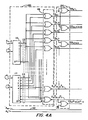
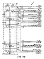
- a conventional decoder 100 selects one of the outputs S0,1-S (2 m -2) , (2 m -1) in response to the address line inputs A1-A m-2 . More specifically, the conventional decoder 100 contains two one-of-N decoders 110, 111, each of which respond to separate sets of address inputs, here one-of-N decoder 110 responds to address Aj-A m-2 and one-of-N decoder 111 responds to address A1-A j-1 .
- the outputs of the one-of-N decoders (112 for decoder 110 and 113 for decoder 111) are normally "high” (i.e., unselected outputs from decoders 110 and 111 are “high") and the selected one of each of the outputs 112, 113 is "low”.
- the NOR array 115 logically ANDs (negative logic) the outputs 112, 113 to produce one "high” output S0,1-S (2 m -2), (2 m -1) , while remaining S0,1-S (2 m -2), (2 m -1) are low.
- the outputs S0,1-S (2 m -2), (2 m -1) of the conventional decoder 100 corresponds to a pair of row lines RL0-RL (2 m -1) (i.e., S0,1 to RL0 and RL1, S2,3 to RL2 and RL3, etc.). Selection of which one of the row lines RL0-RL (2 m -1) corresponding to the enabled one of the outputs S0,1-S (2 m -2), (2 m -1) , occurs in the decoder array 120, in response to the select input S to the decoder array 120.
- the input S is coupled to the address line input A0.
- decoder 100 output S0,1 is “high” and A0 is “low”
- decoder 120a having its select input S “low”
- A0 is “high”
- RL1 would be enabled.
- one of the row lines RL0-RL (2 m -1) is "high” corresponding to the state of the A0 address input and the enabled one of the outputs S0,1-S (2 m -2), (2 m -1) .
- the outputs S0,1-S (2 m -2), (2 m -1) from the conventional decoder 100 also couple to a NOR array 130 which enables a select one of a plurality of row line group select signals GS0-GS (2 m -2), (2 m -1) .
- group select signals designate that a row line RL0-RL (2 m -1) in its corresponding group will be enabled.
- group select signal GS 0,1,2,3,4,5 being enabled (by being "low"), indicates that one of the row address lines RL0-RL5 will be active.
- These group select signals then couple to a NAND array 140 which enables a selected one of the plurality of select lines SL0 ⁇ -SL (2 m -1) ⁇ which corresponds to the selected one of the row address lines RL0-RL (2 m -1) .
- the first group of NAND gates 144 in the NAND array 140 logically ORs together those group select signals GS0-GS (2 m -2),(2 m -1) corresponding to the enabled select lines SL0-SL (2 m -1) .
- NAND gate 144b responds to group select signal GS0, GS 0,1,2,3,4,5 and GS 6,7,8,9 because select address line SL 0,1 and select address line SL 4,5 , which are coupled to NAND gate 144b via NAND gate 154b, correspond to row lines RL0, RL1, RL2 and row lines RL3, RL4, RL5, RL6, respectively.
- Row line RL0-RL (2 m -1) which corresponds to a given select line SL0 ⁇ -SL (2 m -1) ⁇ is shown in parentheses next to the select address line number.
- NAND gate 144c being responsive to group select GS 0,1,2,3,4,5 and group select GS 6,7,8,9 which couples via NAND gate 154c to select address lines SL 2,3 and SL 6,7 .
- Select address line SL 2,3 corresponds to row lines RL1, RL2, RL3, RL4 and select line SL 6,7 corresponds to row lines RL5, RL6, RL7 and RL8.
- the second group of NAND gates 154 enables the select lines SL0 ⁇ -SL (2 m -1) ⁇ such that two memory cells with a common enabled row address line RL0-RL (2 m -1) and common output terminal 37 (FIGS. 2, 3, corresponding to paired memory cells 17 in FIGS.
- two stage address decoding for the row lines RL0-RL (2 m -1) (decoder 100 and decoder 120) provides a "look ahead", or advanced enabling, from decoder 100 for the select line decoders (NOR array 130, NAND array 140).
Landscapes
- Read Only Memory (AREA)
- Semiconductor Memories (AREA)
Claims (4)
- Nichtflüchtiger Speicher als integrierte Schaltung mit folgenden Merkmalen:a) eine Mehrzahl von Auswahlleitungen (SL), die sich in einer Zeilenrichtung erstrecken, und eine Mehrzahl von Bitleitungen (BL), die sich in einer Spaltenrichtung erstrecken, zur Bildung von Zeilen und Spalten von Bereichen, von denen jeder vier Speicherzellen (14) mit einem gemeinsamen Einschaltanschluß (23), vier unabhängige Ausgangsanschlüsse (24) und unabhängige Adressanschlüsse (31) besitzt, die zwischen dem gemeinsamen Einschaltanschluß (23) und jedem der entsprechenden unabhängigen Ausgangsanschlüsse (24) gelegen ist, so daß die unabhängigen Adressanschlüsse (31) zwei Reihen von zwei unabhängigen Adressanschlüssen in jedem Bereich bilden;b) die Mehrzahl von Bitleitungen (BL) hat Verbindung mit entsprechenden Spalten der unabhängigen Ausgangsanschlüsse in solcher Weise, daß in jedem Bereich ein erstes Paar von den vier unabhängigen Ausgangsanschlüssen Verbindung mit einer benachbarten Bitleitung (BL) hat und ein zweites, davon verschiedenes Paar der vier unabhängigen Ausgangsanschlüsse Verbindung mit einer anderen benachbarten Bitleitung hat;c) die Mehrzahl von Auswahlleitungen (SL), die sich in der Zeilenrichtung erstrecken, haben mit den gemeinsamen Einschaltanschlüßen in den Bereichen Verbindung; undd) eine Mehrzahl von Zeilenleitungen (RL) hat Verbindung mit entsprechenden Reihen von unabhängigen Adressanschlüssen (31) in den gebildeten Bereichen, wobei die Anordnung so getroffen ist, daß eine ausgewählte Zeile von Bereichen mit gemeinsamen Einschaltanschlüssen (23) mit jeweils ersten der gemeinsamen Einschaltanschlüsse (23) in alternierender Ordnung an eine erste jeweils benachbarte der Mehrzahl von Auswahlleitungen (SL) angeschlossen ist, und mit jeweils zweiten der gemeinsamen Einschaltanschlüsse (23) in alternierender Ordnung an eine zweite benachbarte der Mehrzahl von Auswahlleitungen (SL) angeschlossen ist.
- Nichtflüchtiger Speicher als integrierte Schaltung gemäß Anspruch 1, dadurch gekennzeichnet, daß jede Speicherzelle (14) einen Feldeffekttransistor enthält.
- Nichtflüchtiger Speicher als integrierte Schaltung mit einem virtuell erdenden Adressdekoder (16), der mit einer Mehrzahl von Zeilenleitungen (RL) und einer Mehrzahl von Auswahlleitungen (SL) Verbindung hat, wobei jede der Mehrzahl von Zeilenleitungen (RL) und entsprechende der Mehrzahl von Auswahlleitungen (SL) mit einer entsprechenden Zeile paarweise vorgesehener Speicherzellen (14) verbunden sind, um eine Speicherzelle (14) in jedem der Paare von Speicherzellen (14) in einer entsprechenden Zeile der paarweise vorgesehenen Speicherzellen (14) auszuwählen, und wobei der Dekoder (16) folgende Merkmale aufweist:
eine Mehrzahl von Eingangsadressleitungen (A₁-Am-2);
ein Eingangsadressenleitungs paar (A₀, Am-1);
eine Dekodiereinrichtung (100), welche mit der Mehrzahl von Eingangsadressleitungen (A₁-Am-2) verbunden ist, um einen von einer Mehrzahl von Ausgängen (S) einzuschalten;
eine erste Auswahleinrichtung (120), die auf die Dekodereinrichtung (100) und auf eine erste (A₀) des Eingangsadressleitungspaars anspricht, um eine ausgewählte der Mehrzahl von Zeilenleitungen (RL) einzuschalten; und
eine zweite Auswahleinrichtung (140), die auf die Mehrzahl von Ausgängen (S) der Dekodiereinrichtung (100) und auf eine zweite (Am-1) des Eingangsadressleitungs Paares anspricht, um eine ausgewählte aus der Mehrzahl von Auswahlleitungen (SL) einzuschalten, welche der ausgewählten Zeilenleitung (RL) entspricht. - Nichtflüchtiger Speicher als integrierte Schaltung gemäß Anspruch 3, dadurch gekennzeichnet, daß benachbarte Zeilenleitungen (RL) zu Gruppen von Zeilenleitungen (RL) geordnet sind und daß die zweiten Auswahleinrichtungen weiter folgende Merkmale enthalten:
Einrichtungen (130), die auf die Dekodiereinrichtung (100) ansprechen, um ein bestimmtes aus einer Mehrzahl von Zeilenleitungsgruppen-Auswahlsignalen (GS) zu erzeugen, wobei die Mehrzahl von Zeilenleitungsgruppen-Auswahlsignalen (GS) den Gruppen von Zeilenleitungen (RL) zugeordnet ist, die durch die erste Auswahleinrichtung (120) eingeschaltet werden; und
eine dritte Auswahleinrichtung (154), die auf die Mehrzahl von Zeilenleitungsgruppen-Auswahlsignalen (GS) und die zweite (Am-1) des Eingangsadressenleitungspaars anspricht, um eine bestimmte der Mehrzahl von Auswahlleitungen (SL) in Entsprechung zu der jeweils ausgewählten der Mehrzahl von Zeilenleitungen (RL) und der zweiten (Am-1) des Eingangsadressenleitungspaares einzuschalten.
Applications Claiming Priority (2)
| Application Number | Priority Date | Filing Date | Title |
|---|---|---|---|
| US81329085A | 1985-12-24 | 1985-12-24 | |
| US813290 | 1985-12-24 |
Publications (3)
| Publication Number | Publication Date |
|---|---|
| EP0227464A2 EP0227464A2 (de) | 1987-07-01 |
| EP0227464A3 EP0227464A3 (en) | 1989-05-31 |
| EP0227464B1 true EP0227464B1 (de) | 1992-05-06 |
Family
ID=25211985
Family Applications (1)
| Application Number | Title | Priority Date | Filing Date |
|---|---|---|---|
| EP86310023A Expired - Lifetime EP0227464B1 (de) | 1985-12-24 | 1986-12-22 | Hochdichter Festwertspeicher |
Country Status (4)
| Country | Link |
|---|---|
| EP (1) | EP0227464B1 (de) |
| JP (1) | JPS62241370A (de) |
| CA (1) | CA1265868A (de) |
| DE (1) | DE3685206D1 (de) |
Citations (2)
| Publication number | Priority date | Publication date | Assignee | Title |
|---|---|---|---|---|
| US4301518A (en) * | 1979-11-01 | 1981-11-17 | Texas Instruments Incorporated | Differential sensing of single ended memory array |
| US4314362A (en) * | 1980-02-04 | 1982-02-02 | Texas Instruments, Incorporated | Power down sequence for electrically programmable memory |
Family Cites Families (1)
| Publication number | Priority date | Publication date | Assignee | Title |
|---|---|---|---|---|
| JPS5819144B2 (ja) * | 1977-12-02 | 1983-04-16 | 株式会社東芝 | 読み出し専用記憶装置 |
-
1986
- 1986-12-22 EP EP86310023A patent/EP0227464B1/de not_active Expired - Lifetime
- 1986-12-22 DE DE8686310023T patent/DE3685206D1/de not_active Expired - Fee Related
- 1986-12-23 CA CA000526168A patent/CA1265868A/en not_active Expired - Fee Related
- 1986-12-24 JP JP61316117A patent/JPS62241370A/ja active Granted
Patent Citations (2)
| Publication number | Priority date | Publication date | Assignee | Title |
|---|---|---|---|---|
| US4301518A (en) * | 1979-11-01 | 1981-11-17 | Texas Instruments Incorporated | Differential sensing of single ended memory array |
| US4314362A (en) * | 1980-02-04 | 1982-02-02 | Texas Instruments, Incorporated | Power down sequence for electrically programmable memory |
Also Published As
| Publication number | Publication date |
|---|---|
| JPS62241370A (ja) | 1987-10-22 |
| CA1265868A (en) | 1990-02-13 |
| EP0227464A3 (en) | 1989-05-31 |
| EP0227464A2 (de) | 1987-07-01 |
| DE3685206D1 (de) | 1992-06-11 |
| JPH0563021B2 (de) | 1993-09-09 |
Similar Documents
| Publication | Publication Date | Title |
|---|---|---|
| US4602354A (en) | X-and-OR memory array | |
| US5583808A (en) | EPROM array segmented for high performance and method for controlling same | |
| KR0179361B1 (ko) | 비휘발성 메모리 어레이 | |
| EP0191544B1 (de) | Speicher-CMOS-Dekodier- und Antriebsschaltung | |
| US6262914B1 (en) | Flash memory segmentation | |
| GB2266796A (en) | Method of accessing an electrically programmable memory device | |
| US4719603A (en) | Semiconductor memory having a dynamic level detecting means for detecting a level of a word line | |
| US4599704A (en) | Read only memory circuit | |
| US6577521B2 (en) | Memory architecture and decoder addressing | |
| US5812453A (en) | Programmable semiconductor memory | |
| US4901285A (en) | High density read-only memory | |
| EP0095847B1 (de) | Kompakter Festwertspeicher mit reduzierter Zugriffzeit | |
| US4634893A (en) | FET driver circuit with mask programmable transition rates | |
| US5535153A (en) | Semiconductor device | |
| JPS61267997A (ja) | 半導体回路 | |
| EP0227464B1 (de) | Hochdichter Festwertspeicher | |
| US4402063A (en) | Flip-flop detector array for minimum geometry semiconductor memory apparatus | |
| US4057787A (en) | Read only memory | |
| US20040119105A1 (en) | Ferroelectric memory | |
| EP0365720B1 (de) | Programmierbarer Halbleiterspeicher | |
| US4292547A (en) | IGFET Decode circuit using series-coupled transistors | |
| US5418740A (en) | Semiconductor memory apparatus formed of a plurality of small memory cells arrays having columns of memory cells connected to column selection word lines through selection transistors | |
| US5245566A (en) | Programmable semiconductor | |
| EP0275212B1 (de) | NAND-Stapelfestwertspeicher | |
| JPH0429157B2 (de) |
Legal Events
| Date | Code | Title | Description |
|---|---|---|---|
| PUAI | Public reference made under article 153(3) epc to a published international application that has entered the european phase |
Free format text: ORIGINAL CODE: 0009012 |
|
| AK | Designated contracting states |
Kind code of ref document: A2 Designated state(s): BE DE FR GB IT NL |
|
| PUAL | Search report despatched |
Free format text: ORIGINAL CODE: 0009013 |
|
| AK | Designated contracting states |
Kind code of ref document: A3 Designated state(s): BE DE FR GB IT NL |
|
| 17P | Request for examination filed |
Effective date: 19890906 |
|
| 17Q | First examination report despatched |
Effective date: 19901206 |
|
| ITTA | It: last paid annual fee | ||
| GRAA | (expected) grant |
Free format text: ORIGINAL CODE: 0009210 |
|
| AK | Designated contracting states |
Kind code of ref document: B1 Designated state(s): BE DE FR GB IT NL |
|
| REF | Corresponds to: |
Ref document number: 3685206 Country of ref document: DE Date of ref document: 19920611 |
|
| ITF | It: translation for a ep patent filed | ||
| ET | Fr: translation filed | ||
| PGFP | Annual fee paid to national office [announced via postgrant information from national office to epo] |
Ref country code: FR Payment date: 19921126 Year of fee payment: 7 |
|
| PGFP | Annual fee paid to national office [announced via postgrant information from national office to epo] |
Ref country code: GB Payment date: 19921217 Year of fee payment: 7 |
|
| PGFP | Annual fee paid to national office [announced via postgrant information from national office to epo] |
Ref country code: NL Payment date: 19921231 Year of fee payment: 7 |
|
| PGFP | Annual fee paid to national office [announced via postgrant information from national office to epo] |
Ref country code: BE Payment date: 19930115 Year of fee payment: 7 |
|
| PLBE | No opposition filed within time limit |
Free format text: ORIGINAL CODE: 0009261 |
|
| STAA | Information on the status of an ep patent application or granted ep patent |
Free format text: STATUS: NO OPPOSITION FILED WITHIN TIME LIMIT |
|
| 26N | No opposition filed | ||
| PGFP | Annual fee paid to national office [announced via postgrant information from national office to epo] |
Ref country code: DE Payment date: 19930830 Year of fee payment: 7 |
|
| NLS | Nl: assignments of ep-patents |
Owner name: LITTON SYSTEMS, INC. TE WOODLAND HILLS, CALIFORNIE |
|
| PG25 | Lapsed in a contracting state [announced via postgrant information from national office to epo] |
Ref country code: GB Effective date: 19931222 |
|
| PG25 | Lapsed in a contracting state [announced via postgrant information from national office to epo] |
Ref country code: BE Effective date: 19931231 |
|
| BERE | Be: lapsed |
Owner name: RAYTHEON CY Effective date: 19931231 |
|
| PG25 | Lapsed in a contracting state [announced via postgrant information from national office to epo] |
Ref country code: NL Effective date: 19940701 |
|
| NLV4 | Nl: lapsed or anulled due to non-payment of the annual fee | ||
| GBPC | Gb: european patent ceased through non-payment of renewal fee |
Effective date: 19931222 |
|
| PG25 | Lapsed in a contracting state [announced via postgrant information from national office to epo] |
Ref country code: FR Effective date: 19940831 |
|
| PG25 | Lapsed in a contracting state [announced via postgrant information from national office to epo] |
Ref country code: DE Effective date: 19940901 |
|
| REG | Reference to a national code |
Ref country code: FR Ref legal event code: ST |
|
| PG25 | Lapsed in a contracting state [announced via postgrant information from national office to epo] |
Ref country code: IT Free format text: LAPSE BECAUSE OF NON-PAYMENT OF DUE FEES Effective date: 20051222 |