EP0227348A2 - Inhaltsadressierbare Speicherschaltung und Verfahren - Google Patents
Inhaltsadressierbare Speicherschaltung und Verfahren Download PDFInfo
- Publication number
- EP0227348A2 EP0227348A2 EP86309418A EP86309418A EP0227348A2 EP 0227348 A2 EP0227348 A2 EP 0227348A2 EP 86309418 A EP86309418 A EP 86309418A EP 86309418 A EP86309418 A EP 86309418A EP 0227348 A2 EP0227348 A2 EP 0227348A2
- Authority
- EP
- European Patent Office
- Prior art keywords
- subfield
- content addressable
- content
- cam
- comparand
- Prior art date
- Legal status (The legal status is an assumption and is not a legal conclusion. Google has not performed a legal analysis and makes no representation as to the accuracy of the status listed.)
- Withdrawn
Links
Images


Classifications
-
- G—PHYSICS
- G06—COMPUTING; CALCULATING OR COUNTING
- G06F—ELECTRIC DIGITAL DATA PROCESSING
- G06F16/00—Information retrieval; Database structures therefor; File system structures therefor
- G06F16/90—Details of database functions independent of the retrieved data types
- G06F16/903—Querying
- G06F16/90335—Query processing
- G06F16/90339—Query processing by using parallel associative memories or content-addressable memories
Definitions
- This invention relates generally to digital memory, and more particularly to associative or content addressable memory circuits.
- RAM random access memory
- RAM is responsive to an address bus and a control bus, and generally has a bidirectional data bus.
- An address is put on the address bus by a central processing unit (CPU), direct memory access (DMA) device, or other addressing device.
- the address on the address bus specifies a unique storage location within the RAM.
- the storage location can be a single bit, or a number of associated bits arranged as a word of memory.
- the control bus serves to validate the address on the address bus, and to specify the direction of the data transfer.
- RAM addressing structure is said to be unambiguous in that a RAM address specifies one and only one data storage location. Due to RAM's unambiguous addressing structure, there is an exact relationship between the width of the address field and memory storage capacity.
- RAM is well suited for many digital applications, it is not particularly well suited for use in systems which process associative data. For example, the sequential access to data when addressing RAM can be inefficient for systems involved in pattern recognition, natural language recognition, sparse matrix processing, and database interrogation.
- More general memory devices and systems permit non-contiguous and ambiguous address values.
- Stored values can be distributed throughout memory in a nonsequential manner, and more than one data element can be associated with a single address value.
- CAM content addressable memory
- Storage locations within CAM are addressed by an incoming bit pattern called a comparand. Part of each storage location within the CAM can be considered to contain an associated address, where the remainder of the storage location can be considered to contain associated data.
- the comparand is compared, in parallel, to associated addresses of all storage locations, and if the associated address has the desired relationship to the comparand the associated data at that location can be accessed. Alternatively, the comparand can be compared to the entirety of the storage locations to detect whether the particular bit pattern corresponding to the comparand is stored within the CAM.
- a typical CAM includes a comparand input bus, a control input bus, a match flag output, a bidirectional data bus, and a mask bus.
- a number of comparison operations built into the CAM and selected by the control bus may be allowable, including equality, inequality, less than, greater than, etc.
- the mask bus provides means to mask certain bits of the comparand during a comparison function, and to mask certain bits of the content address during a writing function. For example, upon a comparison function, masked bits can be forced to give a true comparison. Masks are used less frequently with a writing function, since the stored data would be permanently and irrevocably altered.
- a characteristic of CAM which follows from its addressing structure is that ambiguous content addresses may be permitted. In other words, a number of storage locations within the CAM may contain the same associated address. However, when writing to a CAM the decision can be made whether to suppress or allow ambiguous writes. If ambiguous writes are allowed, then multiple responses may result upon a compare. Multiple responses may also result from other comparison functions that do not have unique results, such as greater than or less than operations.
- Multiple responses from a CAM are usually accessed serially.
- the order of access can be determined by the data's position in memory, the value of the content address, or the value of the associated data.
- the amount of memory required by a digital system is often greater than that available on a single device.
- the architecture of the memory system is not limited by the architecture of the memory device.
- a number of individual memory devices are commonly connected horizontally and/or vertically in a matrix configuration.
- the horizontal connection of memory elements increases the effective width of a stored word of memory
- the vertical connection of memory elements increases the number of memory locations available in the memory system.
- the only known commercially available CAM device which tackles the horizontal cascading problem is the Fairchild F100142 4x4 CAM, which has one open emitter line associated with each memory location to convey intersubfield linking information.
- This solution requires one pin per memory location for intersubfield communication, resulting in a chip of very low data storage capacity.
- a modest 1K x 16 CAM system would require 1024 devices, each residing in a 28 pin package and consuming up to 288 mA at 4.2V. This hypothetical memory system would therefore consume over 1.2 kilowatts of power. Such a system is inappropriate for most applications.
- the method to be described includes the horizontal arrangement of a plurality of CAM subfields into a CAM sector.
- a comparand is divided into a number of comparand subfields, each of which is applied to one of the CAM subfields.
- the storage locations within each of the CAM subfields are divided into a content subfield portion, a content subfield location portion, and a linking value portion.
- the comparand subfields are compared to the content subfield portions of an associated CAM subfield to determine whether a content subfield portion contains a value which favorably compares to the incoming comparand subfield.
- a CAM sector match output is developed at the lowest order CAM subfield.
- a practical horizontally cascadable content addressable circuit includes a plurality of storage locations, where each of the storage locations is divided into a content subfield portion, a content subfield location portion, and a linking value portion.
- An incoming bit pattern is compared simultaneously and in parallel with all existing content address bit patterns by means of comparators integral to the content address memory locations of each subfield.
- an incoming intersubfield bit pattern is compared simultaneously and in parallel with all existing linking value bit patterns of each of the storage locations by means of comparators integral to the linking value memory locations of each subfield.
- Match logic is responsive to an enabling input, to the comparand comparators, and to the intersubfield comparators.
- the match logic When enabled, the match logic will develop an enabling output signal when a particular comparand comparator and its associated intersubfield comparator indicate favorable comparisons at that particular single storage location within the content addressable circuit.
- An intersubfield output circuit outputs the content subfield location bit pattern of the matching location and an associated enable signal that indicates that a match has occurred.
- Content subfield values are stored in their respective subfields within a specific data structure. This data structure restricts the multiple occurrence (ambiguity) of values within a subfield. In the most significant subfield only unique values can exist, while in lower order subfields limited multiple occurrences are permitted.
- the architecture of the content addressable memory system embodying the previously described methodology includes a plurality of content addressable memory devices arranged serially from a highest order device to a lowest order device to form a sector.
- the intersubfield linking output bus of a higher order device is coupled to the intersubfield linking input bus of an adjacent, next-lower-order device within the sector.
- the enable output of a higher order device is coupled to the enable input of an adjacent, next-lower-order device within the sector.
- a plurality of sectors are cascaded by coupling corresponding devices in the various sectors to the same comparand subfield bus.
- the lowest order device of each sector may be coupled to a multiple response handling circuit if ambiguous writes are allowed.
- the content subfield location and enable output of the lowest order device of each sector can be used to read associated data from random access memory.
- An advantage of this arrangement is that it provides a method for efficiently horizontally cascading CAM devices.
- the memory location linking method of the present arrangement greatly reduces the number of signal lines required to transfer intersubfield linking information.
- the architecture of the memory system is not limited by the architecture of its constituent CAM devices.
- the number of subfields within a sector can be arbitrarily large, as can be the number of sectors.
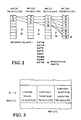
- a horizontally cascaded CAM system in accordance with the present invention includes a plurality of interconnected CAM devices 10.
- a horizontally cascaded CAM device 10 will be hereafter referred to as a HC-CAM 10.
- HC-CAM device and HC-CAM circuit will be used somewhat interchangeably, since the circuitry of a single HC-CAM 10 could be produced either as an integrated circuit, or produced by the interconnection of a plurality of discrete devices.
- the HD-CAMs 10 are arranged in a matrix fashion to create a horizontally cascaded memory system 12.
- the rows of the matrix will be called sectors, and will be referred to with the notation SEC(L) to designate the L th sector.
- the columns of memory system 12 will be called subfields, and will be referenced as SF(K) to designate the K th subfield.
- Adjacent HC-CAMs 10 are linked by intersubfield buses 14. Corresponding HC-CAMs in adjacent sectors are connected to common comparand subfield buses 16. The comparand subfield buses will be referenced with the notation PS(K), where K ranges from 0 to p-1 as previously described. An incoming comparand bus P is the collective of the individual comparand subfields PS(K).
- Each of the memory locations M within the HC-CAMs 10 include a content subfield referenced as TS(K)(L)(M).
- a particular content subfield TS can be referenced by its subfield location (K), its sector location (L), and its location within the sector (M).
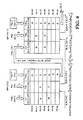
- the data structure of memory system 12 is restricted, and a linking structure is provided.
- the data structure will be described with reference to Fig. 2, and the linking structure will be described with reference to Fig. 3.
- TS(3)(L)(M) content subfields
- TS(0)(L)(M) The highest order content subfield (in this case TS(3)(L)(M) is not permitted to have any ambiguity in its storage locations M. In other words, the same value cannot be stored in more than one content subfield TS(3)(L)(M).
- Fig. 2 where the digit 4 is uniquely stored in TS(3)(L)(0), and the digit 5 is uniquely stored in the location TS(3)(L)(1).
- an ambiguous write is indicated in subfield SF(0) by the asterisk next to content subfield TS(0)(L)(7).
- the same number 4578 has been written in content subfields TS(3)(L)(0), TS(2)(L)(0), TS(1)(L)(0), and TS(0)(L)(0).
- the number 4578 has also been written in content subfields TS(3)(L)(0), TS(2)(L)(0), and TS(1)(L)(0), and TS (0)(L)(7).
- a divergence was permitted at content subfield TS(1)(L)(0) for the ambiguous write.
- ambiguous writes may be permitted. If ambiguous writes are permitted then multiple responses to a comparand P will result when comparing that value.
- a memory location M located in sector SEC(L) and subfield SF(K) is divided into a linking value portion or attribute denoted as LV(K)(L)(M); the aforementioned content subfield portion or attribute TS(K)(L)(M); and a content subfield location portion or attribute denoted as TSL(K)(L)(M).
- the linking value attribute LV(K)(L)(M) and the content subfield location attribute TSL(K+1)(L)(M) provided the proper linking between content subfields TS(K)(L)(M) in adjacent subfields SF(K+1) and SF(K).
- Subfield SF(K) is responsive to an enabling input EIN(K) which enables or disables the subfield.
- the subfield SF(K) is also responsive to an intersubfield bus TSL(K+1), the comparand subfield PS(K), and to a counter TSL ⁇ (K).
- the subfield SF(K) produces an output on an intersubfield bus TSL(K), and an enabling output signal EOUT(K).
- subfield SF(K-1) is responsive to TSL(K), a comparand subfield PS(K-1), a counter TSL ⁇ (K-1), and EIN(K-1) which is equal to EOUT(K).
- Subfield SF(K-1) outputs a TSL(K-1), and an EOUT(K-1).
- each subfield SF(K) the content subfield location TSL(K+1) is compared, in parallel, to the linking values LV(K)(L)(M).
- the incoming comparand subfield PS(K) is compared to the content subfield TS(K)(L)(M).
- sample digits have been associated with the various memory locations of SF(K) and SF(K-1) and with the content subfield locations TSL and the comparand subfields PS for the purpose of discussion.
- the TSL(K+1) bus is indicated to have the value 4
- the PS(K) bus has a value 7.
- TSL(K+1) and LV(K)(L)(M) there is a match between TSL(K+1) and LV(K)(L)(M).
- PS(K) and TS(K)(L)(M) there is a match between PS(K) and TS(K)(L)(M).
- an EOUT(K) EIN(K-1) is produced by subfield SF(K), and a TSL(K) having a value of 2 is input to LV(K-1)(L)(M) of subfield SF(K-1).
- Each subfield SF(K) has the ability to disable all of the lower order subfields beginning with SF(K-1) if there is not a simultaneous match of TSL(K+1) with LV(K)(L)(M) and PS(K) with TS(K)(L)(M).
- the intersubfield bus TSL(K) provides a means for linking a memory location in a subfield SF(K) with a memory location in a subfield SF(K-1).
- the intersubfield linking is repeated from the highest order HC-CAM 10 to the lowest order HC-CAM 10.
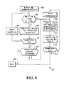
- a flow chart indicates the basic steps taken to write to the HC-CAMS of Fig. 1 so as to create the described data structure.
- Starting block 20 indicates that the writing begins with at the highest order subfield SF(p-1).
- decision block 22 PS is compared to TS and LV is compared to TSL. If both of these conditions are true, the TS value of the matching location is obtained as indicated in block 24.
- the next step, as indicated by decision block 26, is to determine whether the subfield SF is SF(0). If not, the next-less-significant subfield is accessed as indicated by block 28, and the loop of blocks 22-28 is repeated until a comparison at decision block 22 is false or a comparison at decision block 26 is true.
- the TSL of the previous subfield is written to the LV portion of the current subfield, as indicated at block 30.
- the PS value at the current subfield is then written at a memory location determined by TSL ⁇ as indicated at block 32, and then the determination is made whether the next lower subfield is SF(0) at a decision block 34. If it is not, the next lower subfield is selected at block 36 and the loop of blocks 30-36 is repeated until the subfield is SF(0) as determined by decision block 34.
- the writing routine is then exited as indicated at termination block 38.
- Fig. 6 an example is shown which writes the value 56849 across 5 subfields SF(4) to SF(0).
- the loop of blocks 30-36 are thus repeated until the value 56849 has been written across all five subfields.
- the storage efficiency could be defined as the ratio of the storage used for the TS attribute to the total storage required by the device.
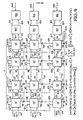
- the HC-CAM 10 ⁇ includes a number of storage locations 42, where each storage location is divided into an LV portion, a TS portion, and a TSL portion.
- HC-CAM 10 ⁇ further includes control logic 44, mask logic 46, match logic 47, a mask latch 48, a TSL ⁇ counter 50, a next-free-address (NFA) stack 52, a multiplexer 54, and HC-CAM full logic 56.
- control logic 44 mask logic 46, match logic 47, a mask latch 48, a TSL ⁇ counter 50, a next-free-address (NFA) stack 52, a multiplexer 54, and HC-CAM full logic 56.
- NFA next-free-address
- HC-CAM 10 ⁇ has a bidirectional bus 58 which can carry the intersubfield linking input bus information ISLI.
- the HC-CAM 10 ⁇ also includes a bidirectional bus 60 which can carry the intersubfield linking output bus information ILSO.
- a bidirectional bus 62 can carry the comparand subfield PS, and an input bus 64 includes a number of control lines.
- An enable input EIN is developed on a line 66, and an enable write to subfield input ES is developed on a line 68.
- the enable output signal EOUT is developed on a line 70, and a subfield full signal SF is developed on a line 72.
- Buses 58, 60, and 62 are bidirectional so that the HC-CAM 10 ⁇ can be read as RAM in a reverse mode. This feature of HC-CAM 10 ⁇ will be discussed subsequently.
- the bus 58 is normally an input bus for ILSI
- the bus 60 is normally an output bus for ILSO
- bus 62 is normally an input bus for PS or for a mask m.
- a mask m is input on bus 62 and an appropriate control signal is input on bus 64 causing mask latch 48 to latch onto the mask m bit pattern.
- the mask m permits certain bits of the TS attribute to be selectively disabled or enabled.
- a comparand PS may be applied to bus 62.
- Mask logic 46 operates on the PS and TS comparison logic according to the contents of mask latch 48.
- Match logic 47 is responsive to the matches between ILSI and the LV attribute, and between the masked PS input and TS attribute as indicated by the brackets and arrow at 74. Match logic 47 is also responsive to EIN on line 66, and develops a signal EOUT on line 70 as previously shown and described with reference to Fig. 4.
- the next memory location 42 is determined by the TSL ⁇ counter 50 and the NFA stack 52, which is preferably a last in, first out (LIFO) type stack. If a memory location 42 had been erased by a previous operation, its address is pushed onto NFA stack 52. Control logic 44, sensing that NFA stack 52 is not empty, will pop the address from the NFA stack 52 and use it for the next TSL value. If the NFA stack is empty, a control logic 44 switches multiplexer 54 such that TSL ⁇ 50 provides the next TSL address.
- TSL ⁇ counter 50 in its simplest form, is a binary up-counter.
- HC-CAM full logic 56 monitors both NFA stack 52 and TSL ⁇ counter 50.
- a subfield full signal SF is developed on line 72.
- the subfield full signal SF on line 72 can be input into the enable write to subfield input ES on a line 68 of a HC-CAM 10 ⁇ in an adjoining sector.
- the HC-CAM 10 ⁇ can be used in a reverse mode as Random Access Memory (RAM). While the random access circuitry for such an operation is not shown herein, the basic method for randomly accessing information from HC-CAMS 10 ⁇ is to input an address on bus 60 which creates a pointer on bus 58 and a TS content subfield output on bus 62. The pointer on bus 58 is used as an input address on a bus 60 of the next-higher-order HC-CAM 10 ⁇ . In this fashion, the HC-CAMS are cascaded in a reverse order, and develop a data output on a comparand bus P which is the collective of the individual outputs on buses 62 of the HC-CAMS 10 ⁇ .
- RAM Random Access Memory
- a number of HC-CAMS 10 ⁇ are coupled together in matrix form creating a memory system having q sectors and p subfields.
- the comparand subfield PS(p-1) is coupled to the bus inputs 62 of all of the HC-CAMS 10 ⁇ in subfield SF(p-1).
- the comparand subfields PS(p-2) to PS(0) are coupled to the input buses 62 of the HC-CAM devices 10 ⁇ of subfields SF(p-2) to SF(0).
- the sharing of the comparand subfield PS(K) for a particular subfield SF(K) is the basic structure for vertically coupling the HC-CAM 10 ⁇ devices.
- a sector enable line 76 is provided between each adjacent sector SEC(L). Coupled to the sector enable lines are the subfield full lines at 72 of the higher order sector, and the enable write to subfield ES line 68 of the adjacent lower order sector.
- the circular symbol 78 signifies a hardwired OR which has the affect of ORing the outputs on lines 72 for a particular sector to develop a resultant on lines 68 of the next-lower-order sector. From a practical point of view, this can be accomplished by making subfield full line 72 on open collector output, such that a low level output on any one of lines 72 will create a low logic level on a sector enable line 76 without damaging the circuitry of the remaining HC-CAMs 10 ⁇ in the sector.
- a bidirectional bus 60 of a higher order HC-CAM 10 ⁇ is coupled directly to bidirectional bus 58 of the next-lower-order HC-CAM 10 ⁇ .
- EOUT line 70 of a higher order HC-CAM 10 ⁇ is coupled to the EIN input lines 66 of the next-lower-order HC-CAM 10 ⁇ .
- the enable write to subfield ES input lines 68 for the HC-CAMs 10 ⁇ of sector SEC(q-1) can be coupled to ground to write enable the first sector SEC(q-1).
- the EIN lines 66 of subfield (p-1) can be wired to V cc to enable HC-CAMs 10 ⁇ along subfield SF(p-1).
- the logic level on input lines 66 and 68 can be controlled by external logic to selectively turn on and off various subfields and sectors.
- the lowest order HC-CAMs of subfield SF(0) may be coupled to multiple response handling circuits 80.
- the multiple response handling circuits 80 are each responsive to the bus 60 of the lowest order HC-CAM 10 ⁇ of a particular sector.
- the multiple response handling circuits 80 are also responsive to the EOUT signal of the lowest order HC-CAM 10 ⁇ of that sector.
- the function of multiple response handling circuits 80 is to allow sequential access to ambiguous writes made in a particular sector. If ambiguous writes were suppressed, the multiple response handling circuits 80 would not be required.
- Multiple response handling circuits 80 output on an address bus 82 and a control line 84.
- RAM 86 is responsive to an address on bus 82 and a control signal on line 84, and is operative to output or input data on a bidirectional data bus 88.
- the multiple response handling circuits 80 can be eliminated, and the RAM can be connected directly to the lowest order HC-CAM 10 ⁇ of each sector. If a match occurs at some content location when a comparand P is applied to the HC-CAM system, a pointer address will be developed on bus 60 and an enable will be developed on line 70 of the lowest order HC-CAM 10 ⁇ to address the associated data in RAM 86.
- the next-less-significant sector will be activated by its associated sector enable line 76.
- the sector enable line 76 of the lowest order sector SEC(0) is activated, a CAM system full signal will be developed as indicated at 90.
- EOUT(0) for a particular sector as developed on line 70 of the HC-CAM in subfield SF(0) can be determined by the following expression:
- This expression is merely an extension of the expression shown with regards to Fig. 4, by taking into account the inputs to the HC-CAMs of the highest order subfield SF(p-1).
Landscapes
- Engineering & Computer Science (AREA)
- Databases & Information Systems (AREA)
- Theoretical Computer Science (AREA)
- Computational Linguistics (AREA)
- Data Mining & Analysis (AREA)
- Physics & Mathematics (AREA)
- General Engineering & Computer Science (AREA)
- General Physics & Mathematics (AREA)
- Debugging And Monitoring (AREA)
- Signal Processing For Digital Recording And Reproducing (AREA)
- Control Of Indicators Other Than Cathode Ray Tubes (AREA)
Applications Claiming Priority (2)
| Application Number | Priority Date | Filing Date | Title |
|---|---|---|---|
| US80757785A | 1985-12-11 | 1985-12-11 | |
| US807577 | 1985-12-11 |
Publications (2)
| Publication Number | Publication Date |
|---|---|
| EP0227348A2 true EP0227348A2 (de) | 1987-07-01 |
| EP0227348A3 EP0227348A3 (de) | 1991-09-25 |
Family
ID=25196712
Family Applications (1)
| Application Number | Title | Priority Date | Filing Date |
|---|---|---|---|
| EP19860309418 Withdrawn EP0227348A3 (de) | 1985-12-11 | 1986-12-03 | Inhaltsadressierbare Speicherschaltung und Verfahren |
Country Status (2)
| Country | Link |
|---|---|
| EP (1) | EP0227348A3 (de) |
| JP (1) | JPS62137799A (de) |
Cited By (5)
| Publication number | Priority date | Publication date | Assignee | Title |
|---|---|---|---|---|
| EP0346918A2 (de) * | 1988-06-17 | 1989-12-20 | Modular Computer Systems Inc. | Vorrichtung für Cache-Speicherverwaltung |
| GB2239114A (en) * | 1987-01-14 | 1991-06-19 | Texas Instruments Ltd | Content addressable memory |
| GB2240678A (en) * | 1990-01-31 | 1991-08-07 | Pioneer Electronic Corp | RDS preset receiver |
| WO1992002932A1 (en) * | 1990-08-02 | 1992-02-20 | Carlstedt Elektronik Ab | Associative memory |
| WO2004021360A1 (en) * | 2002-08-30 | 2004-03-11 | Mosaid Technologies Incorporated | Content addressable memory architecture |
Families Citing this family (1)
| Publication number | Priority date | Publication date | Assignee | Title |
|---|---|---|---|---|
| US6661791B1 (en) * | 1999-12-28 | 2003-12-09 | Mosaid Technologies, Inc. | Method and apparatus for generating forward overrides in a packet switch |
Citations (1)
| Publication number | Priority date | Publication date | Assignee | Title |
|---|---|---|---|---|
| DE3411168A1 (de) * | 1983-04-14 | 1984-10-18 | Wolfgang Dr.-Ing. 6101 Groß-Bieberau Hilberg | Das assoziative feld |
-
1986
- 1986-12-03 EP EP19860309418 patent/EP0227348A3/de not_active Withdrawn
- 1986-12-08 JP JP61292268A patent/JPS62137799A/ja active Pending
Patent Citations (1)
| Publication number | Priority date | Publication date | Assignee | Title |
|---|---|---|---|---|
| DE3411168A1 (de) * | 1983-04-14 | 1984-10-18 | Wolfgang Dr.-Ing. 6101 Groß-Bieberau Hilberg | Das assoziative feld |
Non-Patent Citations (1)
| Title |
|---|
| IEEE CONFERENCE PROCEEDINGS, THE 12TH ANNUAL INTERNATIONAL SYMPOSIUM ON COMPUTER ARCHITECTURE June 17, 1985, BOSTON pages 258-265; DIK LUN LEE: 'A distributed multiple-response resolver for value ordered retrieval ' * |
Cited By (12)
| Publication number | Priority date | Publication date | Assignee | Title |
|---|---|---|---|---|
| GB2239114A (en) * | 1987-01-14 | 1991-06-19 | Texas Instruments Ltd | Content addressable memory |
| GB2239114B (en) * | 1987-01-14 | 1991-09-04 | Texas Instruments Ltd | Content addressable memory |
| EP0346918A2 (de) * | 1988-06-17 | 1989-12-20 | Modular Computer Systems Inc. | Vorrichtung für Cache-Speicherverwaltung |
| EP0346918A3 (de) * | 1988-06-17 | 1991-03-20 | Modular Computer Systems Inc. | Vorrichtung für Cache-Speicherverwaltung |
| GB2240678A (en) * | 1990-01-31 | 1991-08-07 | Pioneer Electronic Corp | RDS preset receiver |
| GB2240678B (en) * | 1990-01-31 | 1994-10-12 | Pioneer Electronic Corp | RDS preset receiver |
| WO1992002932A1 (en) * | 1990-08-02 | 1992-02-20 | Carlstedt Elektronik Ab | Associative memory |
| US5325501A (en) * | 1990-08-02 | 1994-06-28 | Carlstedt Elektronik Ab | Associative memory |
| WO2004021360A1 (en) * | 2002-08-30 | 2004-03-11 | Mosaid Technologies Incorporated | Content addressable memory architecture |
| US6775166B2 (en) | 2002-08-30 | 2004-08-10 | Mosaid Technologies, Inc. | Content addressable memory architecture |
| US7002824B2 (en) | 2002-08-30 | 2006-02-21 | Mosaid Technologies, Inc. | Content addressable memory architecture |
| US7502245B2 (en) | 2002-08-30 | 2009-03-10 | Mosaid Technologies, Inc. | Content addressable memory architecture |
Also Published As
| Publication number | Publication date |
|---|---|
| EP0227348A3 (de) | 1991-09-25 |
| JPS62137799A (ja) | 1987-06-20 |
Similar Documents
| Publication | Publication Date | Title |
|---|---|---|
| EP0054588B1 (de) | Interaktives Datenwiederauffindungsgerät | |
| US4314356A (en) | High-speed term searcher | |
| US4758982A (en) | Quasi content addressable memory | |
| US4575818A (en) | Apparatus for in effect extending the width of an associative memory by serial matching of portions of the search pattern | |
| US4450520A (en) | Method and system for matching encoded characters | |
| US4959811A (en) | Content addressable memory including comparison inhibit and shift register circuits | |
| US4053871A (en) | Method and system for the iterative and simultaneous comparison of data with a group of reference data items | |
| US5010516A (en) | Content addressable memory | |
| JP2511435B2 (ja) | ル−ルベ−スのデ−タ検索方法及び装置 | |
| US4831522A (en) | Circuit and method for page addressing read only memory | |
| US5319762A (en) | Associative memory capable of matching a variable indicator in one string of characters with a portion of another string | |
| US4628483A (en) | One level sorting network | |
| US4783735A (en) | Least recently used replacement level generating apparatus | |
| US4805093A (en) | Content addressable memory | |
| US3505653A (en) | Sorting array | |
| US3290659A (en) | Content addressable memory apparatus | |
| US3483528A (en) | Content addressable memory with means for masking stored information | |
| EP0333346B1 (de) | Bedrahtete Datensortierschaltung | |
| US4254476A (en) | Associative processor | |
| US3389377A (en) | Content addressable memories | |
| EP0227348A2 (de) | Inhaltsadressierbare Speicherschaltung und Verfahren | |
| US4979101A (en) | Apparatus for retrieving character strings | |
| JPS60105039A (ja) | 文字列照合方式 | |
| US3548385A (en) | Adaptive information retrieval system | |
| US4777622A (en) | Associative data storage system |
Legal Events
| Date | Code | Title | Description |
|---|---|---|---|
| PUAI | Public reference made under article 153(3) epc to a published international application that has entered the european phase |
Free format text: ORIGINAL CODE: 0009012 |
|
| AK | Designated contracting states |
Kind code of ref document: A2 Designated state(s): AT BE CH DE ES FR GB GR IT LI LU NL SE |
|
| PUAL | Search report despatched |
Free format text: ORIGINAL CODE: 0009013 |
|
| AK | Designated contracting states |
Kind code of ref document: A3 Designated state(s): AT BE CH DE ES FR GB GR IT LI LU NL SE |
|
| 17P | Request for examination filed |
Effective date: 19911219 |
|
| 17Q | First examination report despatched |
Effective date: 19920605 |
|
| STAA | Information on the status of an ep patent application or granted ep patent |
Free format text: STATUS: THE APPLICATION IS DEEMED TO BE WITHDRAWN |
|
| 18D | Application deemed to be withdrawn |
Effective date: 19930817 |
|
| RIN1 | Information on inventor provided before grant (corrected) |
Inventor name: PRICE, SIMON, |