EP0223260A2 - Signal reading circuit for masked and overlapping linear image sensors - Google Patents
Signal reading circuit for masked and overlapping linear image sensors Download PDFInfo
- Publication number
- EP0223260A2 EP0223260A2 EP86116166A EP86116166A EP0223260A2 EP 0223260 A2 EP0223260 A2 EP 0223260A2 EP 86116166 A EP86116166 A EP 86116166A EP 86116166 A EP86116166 A EP 86116166A EP 0223260 A2 EP0223260 A2 EP 0223260A2
- Authority
- EP
- European Patent Office
- Prior art keywords
- linear image
- image sensors
- storage elements
- storage
- photoelements
- Prior art date
- Legal status (The legal status is an assumption and is not a legal conclusion. Google has not performed a legal analysis and makes no representation as to the accuracy of the status listed.)
- Granted
Links
Images

Classifications
-
- H—ELECTRICITY
- H04—ELECTRIC COMMUNICATION TECHNIQUE
- H04N—PICTORIAL COMMUNICATION, e.g. TELEVISION
- H04N1/00—Scanning, transmission or reproduction of documents or the like, e.g. facsimile transmission; Details thereof
- H04N1/04—Scanning arrangements, i.e. arrangements for the displacement of active reading or reproducing elements relative to the original or reproducing medium, or vice versa
- H04N1/19—Scanning arrangements, i.e. arrangements for the displacement of active reading or reproducing elements relative to the original or reproducing medium, or vice versa using multi-element arrays
- H04N1/191—Scanning arrangements, i.e. arrangements for the displacement of active reading or reproducing elements relative to the original or reproducing medium, or vice versa using multi-element arrays the array comprising a one-dimensional [1D] array
- H04N1/192—Simultaneously or substantially simultaneously scanning picture elements on one main scanning line
- H04N1/193—Simultaneously or substantially simultaneously scanning picture elements on one main scanning line using electrically scanned linear arrays, e.g. linear CCD arrays
- H04N1/1934—Combination of arrays
-
- H—ELECTRICITY
- H04—ELECTRIC COMMUNICATION TECHNIQUE
- H04N—PICTORIAL COMMUNICATION, e.g. TELEVISION
- H04N1/00—Scanning, transmission or reproduction of documents or the like, e.g. facsimile transmission; Details thereof
- H04N1/04—Scanning arrangements, i.e. arrangements for the displacement of active reading or reproducing elements relative to the original or reproducing medium, or vice versa
- H04N1/19—Scanning arrangements, i.e. arrangements for the displacement of active reading or reproducing elements relative to the original or reproducing medium, or vice versa using multi-element arrays
- H04N1/195—Scanning arrangements, i.e. arrangements for the displacement of active reading or reproducing elements relative to the original or reproducing medium, or vice versa using multi-element arrays the array comprising a two-dimensional [2D] array
- H04N1/19505—Scanning picture elements spaced apart from one another in at least one direction
- H04N1/1951—Scanning picture elements spaced apart from one another in at least one direction in one direction
-
- H—ELECTRICITY
- H04—ELECTRIC COMMUNICATION TECHNIQUE
- H04N—PICTORIAL COMMUNICATION, e.g. TELEVISION
- H04N25/00—Circuitry of solid-state image sensors [SSIS]; Control thereof
- H04N25/70—SSIS architectures; Circuits associated therewith
- H04N25/701—Line sensors
-
- H—ELECTRICITY
- H04—ELECTRIC COMMUNICATION TECHNIQUE
- H04N—PICTORIAL COMMUNICATION, e.g. TELEVISION
- H04N25/00—Circuitry of solid-state image sensors [SSIS]; Control thereof
- H04N25/70—SSIS architectures; Circuits associated therewith
- H04N25/701—Line sensors
- H04N25/7013—Line sensors using abutted sensors forming a long line
Definitions
- the present invention relates to a signal reading circuit for linear image sensors such as charge coupled devices, which are connected together in a line to efficiently read the document of large size as well as the document of small size.
- the width of reading by a linear image sensor is usually about 2 to 3 cm. That width of reading is too short for the linear image sensor to read a document of size B5 or A4.
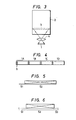
- the reading width 3 of a document 2 is larger than the length of a linear image sensor 1.
- a reduced image of the document 2 is focused on the photoelements of the linear image sensor 1 through a lens unit 4 and then read. For that reason, there is a disadvantage that the optical path length for making the reduced image on the linear image sensor and the size of a reading apparatus are both large.
- a plurality of linear image sensors 1A-1D are disposed in different reading positions so that the total length of the linear image sensors is equal to the teading width of the document. Since the photoresponse properties of the linear image sensors lA-1D need to be set equal to each other, an opaque metalization mask 5 is provided on at least the first photoelement of each of the linear image sensors 1A-1D and the levels of the output signals of the opaque metalized light-intercepted portions of the sensors are made equal to each other to equalize the photoresponse properties of the sensors 1A-1D to each other.
- each of the linear image sensors lA-1D sends out a normalizing signal 91, shown in Fig. 5, laving a dark reference level for the linear image sensor pixel corresponding to the opaque metalization mask 5, and in effective image signal S2 for the remaining pixels. If the output signals of the linear image sensors lA-1D are simply synthesized together, the document 2 cannot exactly be read since the masked pixels do not provide effective image signals.
- a linear image sensor unit 10 As shown by a dot and dash line in Fig. 1 has been developed.
- the linear image sensor unit 10 five linear image sensors 11-15 are disposed so that their reading positions are different from each other not only in a main scanning direction but also in sub-scanning direction perpendicular to the principal linear image sensor direction, and opaque metalized portions 11M-15M of the linear image sensors 11-15 are overlapped with the rear portions of the preceding linear image sensors 11-15.
- the linear image sensor unit 10 sends out, as shown in Fig. 6, a signal Sl having a dark reference level corresponding to one of opaque metalization masks 11M-15M, an effective image signal S2, and a signal S3 corresponding to the overlap of the adjacent linear image sensors. It is a problem how to process the output stignals of the linear image sensor unit 10.
- the present invention is a signal reading circuit for linear image sensors.
- a linear image sensor unit includes a plurality of linear image sensors each having an opaque metalization mask on a photoelement at one end of the linear image sensor. The linear image sensors are disposed so that the reading positions of the linear image sensors are different from each other.
- An A/D converter unit digitizes the output signals of the linear image sensors in parallel with each other. The outputs of the A/D converter unit are stored in storage elements of a line memory, each having a storage capacity not less than the number of the effective photoelements of each linear image sensor. Data obtained by digitizing the output signals of the linear image sensors are sequentially stored from the beginning of the data in parallel with each other in the corresponding storage elements of the line memory.
- the storage starts with the intermediate portion of each storage element rearwards and thereafter returning from the rearmost portion of each storage element to its foremost portion.
- the already written data are sequentially read out of the storage elements of the line memory, starting with the foremost portion of each of the serially connected storage elements of the line memory.
- Fig. 1 shows an embodiment of the present invention.
- Linear image sensors 11-15 which constitute a linear image sensor unit 10, are driven by drive circuits 21-25.
- the output signals of the linear image sensors 11-15 are entered into sample-and-hold circuits 31-35.
- the sampled and held signals are entered into the A/D converters 41-45 of an A/D converter unit 40 so that the signals are converted into digital signals. Since the reading positions of the linear image sensors 11-15 are different from each other in sub-scanning direction transverse to the linear image sensors 11-15) as well as in a main scanning direction, the unprocessed output signals of the linear image sensors would not be identical with signals generated by reading along a single scanned line. However, in reality, the output signals are delayed in the linear image sensors 11-15 or the sample-and-hold oircuits 31-35 so that the output signals are made identical with the signals generated by reading along the single scanned line.
- the A/D converted output of the A/D converter unit 40 is written into one of two line memories 50 and 60 switched by a control circuit not shown in the drawings.
- Serial image signals Pl or P2 are read out of the other of the line memories 60 and 50.
- the control circuit alternately interchanges the two line memories 50 and 60 for writing and reading so that the line memory 60 serves for reading and serial image signals PS2 are read out of the line memory 60 when the data from the A/D converter unit 40 are written into the line memory 50.
- the line memory 50 serves for reading and the already written data are sent as image signals ps1 out of the line memory 50 when the data from the A/D converter unit 40 are written into the line memory 60.
- the output signals of the linear image sensors 11-15 are sampled and held in parallel with each other by the oample-and-hold circuits 31-35.
- the sample-held values are subjected to A/D conversion by the A/D converters 41-45.
- the outputs of the A/D converters are written in parallel with each other into the corresponding storage elements of the line memory 50 or 60 so as to be stored as data therein.
- the image signals PS1 or PS2 are sent in series with each other out of the line memory 60 or 50 to which writing has been already finished.
- An image is read by the linear image sensors 11-15, starting with the positions of opaque metalization masks 11M-15M provided at the left-hand (illustrated in the drawings) ends of the linear image sensors 11-15.
- the digital signals obtained through the sample-and-hole circuits 31-35 and the A/D converters 41-45 are sequentially written into the storage elements 51-55 or 61-65 of the line memory 50 or 60, starting with an intermediate portion of each storage element rearwards and thereafter returning from the rearmost portion of the storage element to its foremost portion.
- the storage element 51 has a storage capacity for the number of the effective (unmasked and non-Overlapped with the following linear image sensor 12) photoelements of the linear image sensor 11 and the storage element 52 has a storage capacity for the number of the effective photoelements of the linear image sensor 12.
- data obtained by digitizing the output signals of the linear image sensor 11 are written into the storage element 51 starting with a beginning address of P1 in the middle of the storage element 51
- data obtained by digitizing the output signals of the linear image sensor 12 are written into the storage element 52 starting with a beginning address of P2 in the middle of the storage element 52.
- a signal having a dark reference level and corresponding to the opaque metalization mask 11M is written into the storage element 51 at the beginning address P1, and an effective image signal is thereafter written into the storage element 51.
- Fig. 1 is shown an example of the control circuitry required for the invention.
- a controller 70 provides the necessary control signals. Timing signals are provided on a line 71 to all the elements.
- a tead/write select signal on a line 72 is provided to the two line memories 50 and 60 and affects them in opposite ways. In synchronism with the timing signal, address signals are provided on line 73 to the line memories 50 and 60.
- each linear image sensor 11-15 has a total number N T of photoelements of which only a number N E are effective because of masking or overlap.
- each of the storage elements 51-55 and 61-65 contain N E storage locations.
- a CCD is a serial read-out device so that N T pulses of the timing signal on line 71 will completely read out the linear image sensors 11-15 beginning with the masked element.
- the line memory 50 or 60 which has been read enabled, sequentially reads out its contents in synchronism with the timing signals as the image signals P61 or PS2.
- Figs. 2(A), 2(B) and 2(C) single-hatched portions show the writing of the signal Sl having the dark reference level, and double-hatched portions show the writing of the effective image signal S2.
- the writing is returned to the foremost portion PS1 of the storage element 51, as shown in Fig. 2(B).
- the address is adjusted so that the effective signal is written into the storage element 51 starting with the foremost portion thereof.
- the effective image signal passes the beginning address Pl, the effective image signal is still written so as to erase the old signal of the dark reference level, as shown in Fig. 2(C).
- the effective image signal is written from the foremost portion of the storage element to its rearmost portion so that only the effective image signals are written into the line memory 50 or 60. For that reason, the unnecessary signals S1 of the dark reference level as shown in Fig. 5 are not included in the image signals P S1 or PS2 serially read out of the line memory 50 or 60.
- each of the storage elements of the line memory may exceed the number of the effective photoelements of the linear image sensor. In that case, reading is not performed out of the surplus storage portion of the storage element.
- a signal reading circuit is provided as described above, so that even if a plurality of linear image sensors are connected together in a long zigzag line, signals can be written into a memory while signals corresponding to the opaque metalization mask portions and overlapped portions of the linear image sensors are being removed. For that reason, serial image data corresponding to the document can be read out of a line memory. If line memories are alternately used for reading and writing, rapid image reading can be performed.
Landscapes
- Engineering & Computer Science (AREA)
- Multimedia (AREA)
- Signal Processing (AREA)
- Facsimile Scanning Arrangements (AREA)
Abstract
Description
- The present invention relates to a signal reading circuit for linear image sensors such as charge coupled devices, which are connected together in a line to efficiently read the document of large size as well as the document of small size.
- The width of reading by a linear image sensor, such as a charge coupled device, is usually about 2 to 3 cm. That width of reading is too short for the linear image sensor to read a document of size B5 or A4. For example, as shown in Fig. 3, the
reading width 3 of adocument 2 is larger than the length of alinear image sensor 1. In order to read thedocument 2 by thelinear image sensor 1, a reduced image of thedocument 2 is focused on the photoelements of thelinear image sensor 1 through alens unit 4 and then read. For that reason, there is a disadvantage that the optical path length for making the reduced image on the linear image sensor and the size of a reading apparatus are both large. - In order to eliminate the disadvantage, a plurality of
linear image sensors 1A-1D, as shown in Fig. 4 are disposed in different reading positions so that the total length of the linear image sensors is equal to the teading width of the document. Since the photoresponse properties of the linear image sensors lA-1D need to be set equal to each other, an opaque metalization mask 5 is provided on at least the first photoelement of each of thelinear image sensors 1A-1D and the levels of the output signals of the opaque metalized light-intercepted portions of the sensors are made equal to each other to equalize the photoresponse properties of thesensors 1A-1D to each other. As a result, each of the linear image sensors lA-1D sends out a normalizing signal 91, shown in Fig. 5, laving a dark reference level for the linear image sensor pixel corresponding to the opaque metalization mask 5, and in effective image signal S2 for the remaining pixels. If the output signals of the linear image sensors lA-1D are simply synthesized together, thedocument 2 cannot exactly be read since the masked pixels do not provide effective image signals. - For that reason, a linear
image sensor unit 10 As shown by a dot and dash line in Fig. 1 has been developed. In the linearimage sensor unit 10, five linear image sensors 11-15 are disposed so that their reading positions are different from each other not only in a main scanning direction but also in sub-scanning direction perpendicular to the principal linear image sensor direction, and opaque metalizedportions 11M-15M of the linear image sensors 11-15 are overlapped with the rear portions of the preceding linear image sensors 11-15. The linearimage sensor unit 10 sends out, as shown in Fig. 6, a signal Sl having a dark reference level corresponding to one ofopaque metalization masks 11M-15M, an effective image signal S2, and a signal S3 corresponding to the overlap of the adjacent linear image sensors. It is a problem how to process the output stignals of the linearimage sensor unit 10. - It is an object of the present invention to provide a signal reading circuit capable of exactly and rapidly processing the output signals of an overlapped, masked linear image sensor unit.
- The present invention is a signal reading circuit for linear image sensors. A linear image sensor unit includes a plurality of linear image sensors each having an opaque metalization mask on a photoelement at one end of the linear image sensor. The linear image sensors are disposed so that the reading positions of the linear image sensors are different from each other. An A/D converter unit digitizes the output signals of the linear image sensors in parallel with each other. The outputs of the A/D converter unit are stored in storage elements of a line memory, each having a storage capacity not less than the number of the effective photoelements of each linear image sensor. Data obtained by digitizing the output signals of the linear image sensors are sequentially stored from the beginning of the data in parallel with each other in the corresponding storage elements of the line memory. The storage starts with the intermediate portion of each storage element rearwards and thereafter returning from the rearmost portion of each storage element to its foremost portion. The already written data are sequentially read out of the storage elements of the line memory, starting with the foremost portion of each of the serially connected storage elements of the line memory.
- The invention is described in detail below with reference to drawings which illustrate preferred embodiments, in which
- Fig. 1 shows a circuit diagram of an embodiment of the present invention,
- Figs. 2(A), 2(B) and 2(C) are drawings for explaining an example of operation of the embodiment,
- Fig. 3 shows a view of an example of reading the document by a linear image sensor,
- Fig. 4 shows an example of a linear image sensor unit consisting of linear image sensors connected in series with each other, and
- Figs, 5 and 6 are drawings for explaining the output of data from linear image sensors.
- Fig. 1 shows an embodiment of the present invention. Linear image sensors 11-15, which constitute a linear
image sensor unit 10, are driven by drive circuits 21-25. The output signals of the linear image sensors 11-15 are entered into sample-and-hold circuits 31-35. The sampled and held signals are entered into the A/D converters 41-45 of an A/D converter unit 40 so that the signals are converted into digital signals. Since the reading positions of the linear image sensors 11-15 are different from each other in sub-scanning direction transverse to the linear image sensors 11-15) as well as in a main scanning direction, the unprocessed output signals of the linear image sensors would not be identical with signals generated by reading along a single scanned line. However, in reality, the output signals are delayed in the linear image sensors 11-15 or the sample-and-hold oircuits 31-35 so that the output signals are made identical with the signals generated by reading along the single scanned line. - The A/D converted output of the A/
D converter unit 40 is written into one of twoline memories line memories line memories line memory 60 serves for reading and serial image signals PS2 are read out of theline memory 60 when the data from the A/D converter unit 40 are written into theline memory 50. Similarly, theline memory 50 serves for reading and the already written data are sent as image signals ps1 out of theline memory 50 when the data from the A/D converter unit 40 are written into theline memory 60. According to the present invention, the output signals of the linear image sensors 11-15 are sampled and held in parallel with each other by the oample-and-hold circuits 31-35. The sample-held values are subjected to A/D conversion by the A/D converters 41-45. The outputs of the A/D converters are written in parallel with each other into the corresponding storage elements of theline memory line memory - An image is read by the linear image sensors 11-15, starting with the positions of
opaque metalization masks 11M-15M provided at the left-hand (illustrated in the drawings) ends of the linear image sensors 11-15. The digital signals obtained through the sample-and-hole circuits 31-35 and the A/D converters 41-45 are sequentially written into the storage elements 51-55 or 61-65 of theline memory storage element 51 has a storage capacity for the number of the effective (unmasked and non-Overlapped with the following linear image sensor 12) photoelements of thelinear image sensor 11 and thestorage element 52 has a storage capacity for the number of the effective photoelements of thelinear image sensor 12. As shown in Fig. 2(A) data obtained by digitizing the output signals of thelinear image sensor 11 are written into thestorage element 51 starting with a beginning address of P1 in the middle of thestorage element 51, and data obtained by digitizing the output signals of thelinear image sensor 12 are written into thestorage element 52 starting with a beginning address of P2 in the middle of thestorage element 52. For that reason, for thestorage element 51, a signal having a dark reference level and corresponding to theopaque metalization mask 11M is written into thestorage element 51 at the beginning address P1, and an effective image signal is thereafter written into thestorage element 51. - In Fig. 1 is shown an example of the control circuitry required for the invention. A
controller 70 provides the necessary control signals. Timing signals are provided on a line 71 to all the elements. A tead/write select signal on a line 72 is provided to the twoline memories line memories - Assume that each linear image sensor 11-15 has a total number NT of photoelements of which only a number NE are effective because of masking or overlap. Assume also that each of the storage elements 51-55 and 61-65 contain NE storage locations. A CCD is a serial read-out device so that NT pulses of the timing signal on line 71 will completely read out the linear image sensors 11-15 beginning with the masked element. In synchronism with these NT pulses, the address signals on the line 73 to the
line memory storage element - The
line memory - In Figs. 2(A), 2(B) and 2(C), single-hatched portions show the writing of the signal Sl having the dark reference level, and double-hatched portions show the writing of the effective image signal S2. After the writing into the rearmost portion pE1 of the
storage element 51 is completed, the writing is returned to the foremost portion PS1 of thestorage element 51, as shown in Fig. 2(B). At that time, the address is adjusted so that the effective signal is written into thestorage element 51 starting with the foremost portion thereof. After the effective image signal passes the beginning address Pl, the effective image signal is still written so as to erase the old signal of the dark reference level, as shown in Fig. 2(C). Into each storage element having the storage capacity for the number of the effective photoelements of the linear image sensor, the effective image signal is written from the foremost portion of the storage element to its rearmost portion so that only the effective image signals are written into theline memory line memory - Although five linear image sensors are connected in series with each other in the embodiment described above, the number of the linear image sensors is optional. The storage capacity of each of the storage elements of the line memory may exceed the number of the effective photoelements of the linear image sensor. In that case, reading is not performed out of the surplus storage portion of the storage element.
- According to the present invention, a signal reading circuit is provided as described above, so that even if a plurality of linear image sensors are connected together in a long zigzag line, signals can be written into a memory while signals corresponding to the opaque metalization mask portions and overlapped portions of the linear image sensors are being removed. For that reason, serial image data corresponding to the document can be read out of a line memory. If line memories are alternately used for reading and writing, rapid image reading can be performed.
Claims (6)
Applications Claiming Priority (2)
| Application Number | Priority Date | Filing Date | Title |
|---|---|---|---|
| JP262974/85 | 1985-11-22 | ||
| JP60262974A JPS62122461A (en) | 1985-11-22 | 1985-11-22 | Read circuit for line sensor |
Publications (3)
| Publication Number | Publication Date |
|---|---|
| EP0223260A2 true EP0223260A2 (en) | 1987-05-27 |
| EP0223260A3 EP0223260A3 (en) | 1989-03-08 |
| EP0223260B1 EP0223260B1 (en) | 1994-02-02 |
Family
ID=17383133
Family Applications (1)
| Application Number | Title | Priority Date | Filing Date |
|---|---|---|---|
| EP86116166A Expired - Lifetime EP0223260B1 (en) | 1985-11-22 | 1986-11-21 | Signal reading circuit for masked and overlapping linear image sensors |
Country Status (4)
| Country | Link |
|---|---|
| US (1) | US4754338A (en) |
| EP (1) | EP0223260B1 (en) |
| JP (1) | JPS62122461A (en) |
| DE (1) | DE3689610T2 (en) |
Cited By (3)
| Publication number | Priority date | Publication date | Assignee | Title |
|---|---|---|---|---|
| GB2213346A (en) * | 1987-12-25 | 1989-08-09 | Fuji Xerox Co Ltd | Original document reading apparatus |
| EP0284043A3 (en) * | 1987-03-24 | 1989-10-18 | Dainippon Screen Mfg. Co., Ltd. | Method of and apparatus for connecting output image signals from a plurality of line image sensors |
| FR2755337A1 (en) * | 1996-10-25 | 1998-04-30 | Council Cent Lab Res Councils | CAMERA SYSTEM |
Families Citing this family (6)
| Publication number | Priority date | Publication date | Assignee | Title |
|---|---|---|---|---|
| JPS63191469A (en) * | 1987-02-03 | 1988-08-08 | Toshiba Corp | Image reader |
| EP0292253B1 (en) * | 1987-05-22 | 1992-03-18 | Oki Electric Industry Company, Limited | Contact-type image scanner |
| US4984085A (en) * | 1989-08-03 | 1991-01-08 | Allen-Bradley Company, Inc. | Image processor with dark current compensation |
| JPH0435177A (en) * | 1990-05-25 | 1992-02-05 | Suzuki Motor Corp | Ccd drive circuit |
| US5264945A (en) * | 1991-10-16 | 1993-11-23 | Eastman Kodak Company | Contact array scanners with circulating memory |
| CA2126064A1 (en) * | 1993-06-17 | 1994-12-18 | Jean-Francois Meunier | Apparatus and method for converting a visible image of an object into a digital representation |
Family Cites Families (16)
| Publication number | Priority date | Publication date | Assignee | Title |
|---|---|---|---|---|
| US4249217A (en) * | 1979-05-29 | 1981-02-03 | International Business Machines Corporation | Separated sensor array abutment |
| US4370641A (en) * | 1979-08-15 | 1983-01-25 | International Business Machines Corporation | Electronic control system |
| US4536801A (en) * | 1981-10-01 | 1985-08-20 | Banctec, Inc. | Video data compression system and method |
| DE3200838C2 (en) * | 1982-01-14 | 1984-09-06 | Messerschmitt-Bölkow-Blohm GmbH, 8012 Ottobrunn | Device for reading out detector lines in a one- or two-dimensional arrangement |
| GB2122833B (en) * | 1982-06-24 | 1985-06-26 | Ferranti Plc | Radiation detecting apparatus |
| JPS5986379A (en) * | 1982-11-08 | 1984-05-18 | Toshiba Corp | Photoelectric converter |
| DE3241752C2 (en) * | 1982-11-11 | 1984-09-06 | Messerschmitt-Bölkow-Blohm GmbH, 8012 Ottobrunn | Directional stabilized image field scanning |
| FR2538651B1 (en) * | 1982-12-23 | 1986-08-22 | Thomson Csf | METHOD FOR MODULATING THE SENSITIVITY OF A LINE TRANSFER PHOTOSENSITIVE DEVICE AND DEVICE IMPLEMENTING SAID METHOD |
| US4639608A (en) * | 1983-05-18 | 1987-01-27 | Canon Kabushiki Kaisha | Image read-out apparatus with light source driving means |
| DE3427659A1 (en) * | 1983-07-29 | 1985-02-07 | Canon K.K., Tokio/Tokyo | TEMPLATE READER |
| US4590521A (en) * | 1983-08-19 | 1986-05-20 | Advanced Micro Devices, Inc. | Picture element generator for facsimile receiver |
| US4691114A (en) * | 1984-02-29 | 1987-09-01 | Canon Kabushiki Kaisha | Original reader with variable magnification and time delay |
| CA1263175A (en) * | 1984-05-28 | 1989-11-21 | Hideyuki Miyazawa | Image reader for image processing apparatus |
| JPS6197619A (en) * | 1984-10-19 | 1986-05-16 | Fuji Photo Film Co Ltd | Optical linear encoder |
| US4652743A (en) * | 1984-11-30 | 1987-03-24 | Brother Kogyo Kabushiki Kaisha | Optical image-reading apparatus |
| DE3716152A1 (en) * | 1987-05-14 | 1988-11-24 | Standard Elektrik Lorenz Ag | FLOORING CONNECTOR FITTED ON A MOUNTING PLATE |
-
1985
- 1985-11-22 JP JP60262974A patent/JPS62122461A/en active Granted
-
1986
- 1986-11-21 DE DE86116166T patent/DE3689610T2/en not_active Expired - Fee Related
- 1986-11-21 EP EP86116166A patent/EP0223260B1/en not_active Expired - Lifetime
- 1986-11-24 US US06/934,578 patent/US4754338A/en not_active Expired - Lifetime
Cited By (6)
| Publication number | Priority date | Publication date | Assignee | Title |
|---|---|---|---|---|
| EP0284043A3 (en) * | 1987-03-24 | 1989-10-18 | Dainippon Screen Mfg. Co., Ltd. | Method of and apparatus for connecting output image signals from a plurality of line image sensors |
| GB2213346A (en) * | 1987-12-25 | 1989-08-09 | Fuji Xerox Co Ltd | Original document reading apparatus |
| GB2213346B (en) * | 1987-12-25 | 1992-07-22 | Fuji Xerox Co Ltd | Original document reading apparatus |
| US5148296A (en) * | 1987-12-25 | 1992-09-15 | Fuji Xerox Co., Ltd. | Original document reading apparatus |
| FR2755337A1 (en) * | 1996-10-25 | 1998-04-30 | Council Cent Lab Res Councils | CAMERA SYSTEM |
| US7102664B2 (en) | 1996-10-25 | 2006-09-05 | The Council For The Central Laboratory Of The Research Councils | Camera system |
Also Published As
| Publication number | Publication date |
|---|---|
| DE3689610D1 (en) | 1994-03-17 |
| US4754338A (en) | 1988-06-28 |
| EP0223260B1 (en) | 1994-02-02 |
| JPH0516781B2 (en) | 1993-03-05 |
| DE3689610T2 (en) | 1994-05-11 |
| EP0223260A3 (en) | 1989-03-08 |
| JPS62122461A (en) | 1987-06-03 |
Similar Documents
| Publication | Publication Date | Title |
|---|---|---|
| US7430006B2 (en) | Charge transfer device and a driving method thereof and a driving method for solid-state image sensing device | |
| US6473538B2 (en) | Image sensor | |
| EP0091798A2 (en) | Solid state image sensor | |
| US5689347A (en) | Signal processing apparatus | |
| US4754338A (en) | Signal reading circuit for masked and overlapping linear image sensors | |
| US6288744B1 (en) | Solid-state image pickup device with a shared shift register and method of driving the same | |
| JP3165731B2 (en) | Image reading device | |
| US20020054230A1 (en) | Method for controlling a charge-coupled device sensing module | |
| US7365888B2 (en) | Image read apparatus | |
| US6356305B1 (en) | Image-pickup apparatus and method for reading accumulated signal changes through transfer lines | |
| JP3581554B2 (en) | Image sensor and image reading device | |
| US7816636B2 (en) | Image reading apparatus having a rearranging section providing addresses for accessing to a storage section | |
| JP3130822B2 (en) | Image input device | |
| US6765699B1 (en) | Photosensor array with decreased scan time for decreased optical sampling rates | |
| EP0308624A2 (en) | Solid state imaging device for providing line decimated output | |
| US5283669A (en) | Reading apparatus using two readout circuits connected in reverse order | |
| JP2829007B2 (en) | Image sensor device | |
| JP3607866B2 (en) | Imaging device | |
| JP4039329B2 (en) | Image reading apparatus and data output method in image reading apparatus | |
| US12096138B2 (en) | Quasi-global shutter for image sensors | |
| JP4135606B2 (en) | Image processing device | |
| JP3944073B2 (en) | Photoelectric conversion device and image sensor | |
| JPS6016760A (en) | Original reading device | |
| JPS60171862A (en) | Image reading device | |
| JP2940802B2 (en) | Solid-state imaging device and driving method thereof |
Legal Events
| Date | Code | Title | Description |
|---|---|---|---|
| PUAI | Public reference made under article 153(3) epc to a published international application that has entered the european phase |
Free format text: ORIGINAL CODE: 0009012 |
|
| AK | Designated contracting states |
Kind code of ref document: A2 Designated state(s): DE FR GB |
|
| PUAL | Search report despatched |
Free format text: ORIGINAL CODE: 0009013 |
|
| AK | Designated contracting states |
Kind code of ref document: A3 Designated state(s): DE FR GB |
|
| 17P | Request for examination filed |
Effective date: 19890317 |
|
| 17Q | First examination report despatched |
Effective date: 19920320 |
|
| GRAA | (expected) grant |
Free format text: ORIGINAL CODE: 0009210 |
|
| AK | Designated contracting states |
Kind code of ref document: B1 Designated state(s): DE FR GB |
|
| REF | Corresponds to: |
Ref document number: 3689610 Country of ref document: DE Date of ref document: 19940317 |
|
| ET | Fr: translation filed | ||
| PLBE | No opposition filed within time limit |
Free format text: ORIGINAL CODE: 0009261 |
|
| STAA | Information on the status of an ep patent application or granted ep patent |
Free format text: STATUS: NO OPPOSITION FILED WITHIN TIME LIMIT |
|
| 26N | No opposition filed | ||
| REG | Reference to a national code |
Ref country code: GB Ref legal event code: IF02 |
|
| PGFP | Annual fee paid to national office [announced via postgrant information from national office to epo] |
Ref country code: FR Payment date: 20021108 Year of fee payment: 17 |
|
| PGFP | Annual fee paid to national office [announced via postgrant information from national office to epo] |
Ref country code: GB Payment date: 20021120 Year of fee payment: 17 |
|
| PGFP | Annual fee paid to national office [announced via postgrant information from national office to epo] |
Ref country code: DE Payment date: 20021121 Year of fee payment: 17 |
|
| PG25 | Lapsed in a contracting state [announced via postgrant information from national office to epo] |
Ref country code: GB Free format text: LAPSE BECAUSE OF NON-PAYMENT OF DUE FEES Effective date: 20031121 |
|
| PG25 | Lapsed in a contracting state [announced via postgrant information from national office to epo] |
Ref country code: DE Free format text: LAPSE BECAUSE OF NON-PAYMENT OF DUE FEES Effective date: 20040602 |
|
| GBPC | Gb: european patent ceased through non-payment of renewal fee |
Effective date: 20031121 |
|
| PG25 | Lapsed in a contracting state [announced via postgrant information from national office to epo] |
Ref country code: FR Free format text: LAPSE BECAUSE OF NON-PAYMENT OF DUE FEES Effective date: 20040730 |
|
| REG | Reference to a national code |
Ref country code: FR Ref legal event code: ST |