EP0222388A2 - Laser scanning apparatus - Google Patents
Laser scanning apparatus Download PDFInfo
- Publication number
- EP0222388A2 EP0222388A2 EP86115710A EP86115710A EP0222388A2 EP 0222388 A2 EP0222388 A2 EP 0222388A2 EP 86115710 A EP86115710 A EP 86115710A EP 86115710 A EP86115710 A EP 86115710A EP 0222388 A2 EP0222388 A2 EP 0222388A2
- Authority
- EP
- European Patent Office
- Prior art keywords
- laser scanning
- scanning apparatus
- photodetector
- radiograph
- field
- Prior art date
- Legal status (The legal status is an assumption and is not a legal conclusion. Google has not performed a legal analysis and makes no representation as to the accuracy of the status listed.)
- Granted
Links
Images

Classifications
-
- H—ELECTRICITY
- H04—ELECTRIC COMMUNICATION TECHNIQUE
- H04N—PICTORIAL COMMUNICATION, e.g. TELEVISION
- H04N1/00—Scanning, transmission or reproduction of documents or the like, e.g. facsimile transmission; Details thereof
- H04N1/04—Scanning arrangements, i.e. arrangements for the displacement of active reading or reproducing elements relative to the original or reproducing medium, or vice versa
- H04N1/06—Scanning arrangements, i.e. arrangements for the displacement of active reading or reproducing elements relative to the original or reproducing medium, or vice versa using cylindrical picture-bearing surfaces, i.e. scanning a main-scanning line substantially perpendicular to the axis and lying in a curved cylindrical surface
- H04N1/0607—Scanning a concave surface, e.g. with internal drum type scanners
- H04N1/0621—Scanning a concave surface, e.g. with internal drum type scanners using a picture-bearing surface stationary in the main-scanning direction
- H04N1/0635—Scanning a concave surface, e.g. with internal drum type scanners using a picture-bearing surface stationary in the main-scanning direction using oscillating or rotating mirrors
-
- H—ELECTRICITY
- H04—ELECTRIC COMMUNICATION TECHNIQUE
- H04N—PICTORIAL COMMUNICATION, e.g. TELEVISION
- H04N1/00—Scanning, transmission or reproduction of documents or the like, e.g. facsimile transmission; Details thereof
- H04N1/024—Details of scanning heads ; Means for illuminating the original
- H04N1/028—Details of scanning heads ; Means for illuminating the original for picture information pick-up
- H04N1/03—Details of scanning heads ; Means for illuminating the original for picture information pick-up with photodetectors arranged in a substantially linear array
- H04N1/031—Details of scanning heads ; Means for illuminating the original for picture information pick-up with photodetectors arranged in a substantially linear array the photodetectors having a one-to-one and optically positive correspondence with the scanned picture elements, e.g. linear contact sensors
- H04N1/0313—Direct contact pick-up heads, i.e. heads having no array of elements to project the scanned image elements onto the photodectors
-
- H—ELECTRICITY
- H04—ELECTRIC COMMUNICATION TECHNIQUE
- H04N—PICTORIAL COMMUNICATION, e.g. TELEVISION
- H04N1/00—Scanning, transmission or reproduction of documents or the like, e.g. facsimile transmission; Details thereof
- H04N1/04—Scanning arrangements, i.e. arrangements for the displacement of active reading or reproducing elements relative to the original or reproducing medium, or vice versa
- H04N1/06—Scanning arrangements, i.e. arrangements for the displacement of active reading or reproducing elements relative to the original or reproducing medium, or vice versa using cylindrical picture-bearing surfaces, i.e. scanning a main-scanning line substantially perpendicular to the axis and lying in a curved cylindrical surface
- H04N1/0657—Scanning a transparent surface, e.g. reading a transparency original
-
- H—ELECTRICITY
- H04—ELECTRIC COMMUNICATION TECHNIQUE
- H04N—PICTORIAL COMMUNICATION, e.g. TELEVISION
- H04N1/00—Scanning, transmission or reproduction of documents or the like, e.g. facsimile transmission; Details thereof
- H04N1/04—Scanning arrangements, i.e. arrangements for the displacement of active reading or reproducing elements relative to the original or reproducing medium, or vice versa
- H04N1/06—Scanning arrangements, i.e. arrangements for the displacement of active reading or reproducing elements relative to the original or reproducing medium, or vice versa using cylindrical picture-bearing surfaces, i.e. scanning a main-scanning line substantially perpendicular to the axis and lying in a curved cylindrical surface
- H04N1/0664—Scanning arrangements, i.e. arrangements for the displacement of active reading or reproducing elements relative to the original or reproducing medium, or vice versa using cylindrical picture-bearing surfaces, i.e. scanning a main-scanning line substantially perpendicular to the axis and lying in a curved cylindrical surface with sub-scanning by translational movement of the picture-bearing surface
-
- H—ELECTRICITY
- H04—ELECTRIC COMMUNICATION TECHNIQUE
- H04N—PICTORIAL COMMUNICATION, e.g. TELEVISION
- H04N2201/00—Indexing scheme relating to scanning, transmission or reproduction of documents or the like, and to details thereof
- H04N2201/04—Scanning arrangements
- H04N2201/0402—Arrangements not specific to a particular one of the scanning methods covered by groups H04N1/04 - H04N1/207
- H04N2201/0404—Scanning transparent media, e.g. photographic film
Definitions
- the present invention relates to a laser scanning apparatus for scanning a radiograph, and in particular to a laser scanning apparatus in which the radiograph is supported on a curved field and which includes a curvilinear photodetector.
- Laser scanning apparatus for scanning a radiograph and digitizing the same for electronic analysis and transmission are known.
- Exemplary of such apparatus is that manufactured by E. I. du Pont de Nemours and Company, Inc. as the Film Digital Radiography System.
- Such apparatus uses a galvanometer based oscillating mirror to direct a beam of interrogating radiation across the surface of a radiograph.
- the radiograph is supported on a planar surface, or platen.
- Mounted above the platen in a position to receive the radiation transmitted through the radiograph is a linear semiconductor photodetector.
- the photodetector is fabricated from a plurality of PIN semiconductor diode strips placed edge-to-edge in a planar orientation.
- An optical diffuser is disposed between the diodes and the platen.
- Such scanners have certain limitations associated therewith.
- the path length to the radiograph changes causing the size of the spot of radiation to vary.
- the mirror scans at constant angular velocity, the velocity of the spot along the planar radiograph varies. This causes a geometric distortion of the acquired image.
- the shape of the spot of incident radiation is also distorted, thus degrading resolution.
- the absorption of the beam are known to occur.
- the prior system is slow, taking approximately one minute to scan a typical radiograph, owing primarily to the limited speed of oscillation of the galvanometer mirror.
- Curved fields are known in the facsimile arts, as evidenced by United States Patent 3,370,504.
- This patent discloses a facsimile apparatus which has a curved field and which has positioned therebehind a correspondingly curved array of optical fibers.
- the fibers conduct the transmitted radiation to a single photosensor, typically a photomultiplier tube.
- a recognized limitation of such an arrangement is a limited signal to noise ratio due to the noise introduced by the irregular effects resulting from the light passing from one optical fiber to the next.
- Photomultiplier tubes also have known limitations, such as, their sensitivity to mechanical vibration, their tendency to degrade with age and their inability to tolerate excessive light levels. These factors presently militate against the use of this type of detector in precision medical uses.
- the present invention relates to a laser scanning apparatus comprising a curved field formed of spaced, coaxial plates for receiving a radiograph to be scanned by radiation produced from a laser source.
- One of the plates is formed of an optically diffuse material.
- Means, such as a rotatable multifaceted mirror and beam forming optics, is provided to produce a focussed beam of interrogating radiation on the radiograph.
- the source and beam forming means are mounted on a gantry that is displaceable with respect to the field to cause the beam to scan the field in raster fashion.
- a photodetector is positioned with respect to the field to receive radiation transmitted through the radiograph.
- the photodetector is itself comprised of a plurality of semiconductor elements connected electrically in parallel and physically arranged in edge-to-edge abutting relationship.
- the elements are arranged in a curvilinear pattern with each being substantially equally spaced from the radiograph.
- a slit may be mounted intermediate the field and the photodetector.
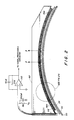
- FIG. 1 shows a highly stylized pictorial representation of a laser scanning apparatus or scanner 10 in accordance with the present invention.
- the scanner 10 includes a base 14 that supports a film guide generally indicated by reference character 16.
- the film guide 16 includes an inlet chute 18 that communicates with a curved film support arrangement 20.
- the film support arrangement includes a pair of curved plates 22 and 24 arranged in a coaxial orientation to each other.
- the inner plate 22 is formed of clear glass that has an antireflection coating on both sides.
- the outer plate 24 is formed of an optically diffuse material such as opal glass.
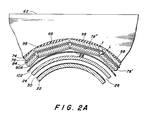
- the plates 22 and 24 are spaced from each other by a predetermined clearance distance to form a curved film transport passage 26 (Figure 2A).
- the passage 26 is in communication with the chute 18.
- the end of the passage 26 opposite the chute 18 is intermittently closable by a film stop member 28.
- the stop 28 When asserted the stop 28 provides an abutment against which a radiographic film 30 to be scanned in a manner to be discussed is maintained in a predetermined position.
- the plates 22, 24 thus cooperate to define a curved field for receiving the radiograph to be scanned.
- the outlet of the passage may communicate with a suitable receptacle (not shown).
- a laser source 34 operative to project a beam 36 of radiation through beam forming optics 42 toward a pair of reflecting elements 38, 40.
- a suitable reference photodetector may be provided at an appropriate location for compensating any power variations in the laser source. Such a compensating reference device is omitted from the figure for clarity.
- a typical compensating reference device is shown in United States Patent 3,741,664, which is incorporated by reference herein..
- the beam is deflected by the operation of the elements 38, 40 also mounted on the gantry 32.
- the beam passes to a rotatable multifaceted mirror 44.
- the mirror 44 is mounted for rotation movement in a housing 46 also supported on the gantry 32. As the incoming beam 36 impinges on a facet of the mirror presented thereto a beam 48 of interrogating radiation is directed toward the film 30 supported in the support arrangement 20 defined by the plates 22, 24.
- the elements 34, 38, 40, 42 and 44 comprise means for producing a focussed beam 48 of interrogating radiation on the radiographic film 30. It should be readily appreciated that these means may be implemented by alternative scanning devices to cause the scanning beam 48 to remain at a focus as the beam 48 sweeps across the radiograph 30. Such alternatives may include acoustic-optic, holographic and/or other electro-optic devices to cause the beam to scan at a known angular rate.
- the gantry 32 is displaceable by a synchronous motor drive (shown schematically at 55) on a pair of guide rails in the direction of the double-headed arrow 58.
- the motor 55 and guide rails may be conveniently mounted anywhere on the scanner 10, as beneath the gantry 32 on the base 14.
- the film guide 16 is supported on rods 56 which are themselves supported on pillars 60.
- the pillars 60 are fixed to the base 14. As a result the interrogating beam 48 moves relatively to the film 30 disposed between the plates 22, 24 such that the film 30 may be scanned in a raster fashion by the beam 48.
- a photodetector assembly, or arm 62 is supported from the gantry 32 by a post 64.
- the arm 62 is cantilevered over the outer plate 24 and houses a photodetector 66 in accordance with the present invention.
- the arm 62 is provided with a substantially curved inner surface 68.
- the photodetector 66 is received and fixedly supported on the curved surface 68 of the arm 62 so as to lie radially proximal to the optically diffuse plate 24.
- the plate 24 diffuses the radiation transmitted through the radiograph to the photodetector 66.
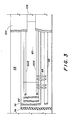
- the photodetector 66 is formed as a laminate structure.
- the lower layer of the photodetector 66 is a substrate 74, such as a circuit board or other rigid member.
- the substrate 74 is notched at predetermined intervals to permit it to closely approximate the curve of the inner surface 68 of the arm 62.
- a first conductor path 76 is disposed on the substrate 74.
- Mounted above the first conductor path 76 is an array of photoresponsive semiconductor elements 78A through 78N. Adjacent ones of the elements 78 are abutted in next adjacency with the leading edge L ( Figure 2A) of a given element (e.g., the element 78') in physical contact with the trailing edge T of the next adjacent element (e.g., the element 78").
- Each element 78 is formed of a body 80 of PIN semiconductor material.
- the lower surface of the body 90 is covered with a metallization 84 that is disposed in electrical contact with the conductor path 76.
- the opposite surface 88 of the semiconductor body has a pair of metallization paths 90A, 90B arranged along the confronting elongated edges thereof.
- a second conductor path 92 is disposed on the substrate 74 in substantially parallel relation to the first conductor path 76. Attachment leads 96 electrically connect the metallization path 90A to the second conductor path 92.
- the above-described photodetector 66 is attached to the curved surface 68 of the arm 62 by any suitable means of attachment, as by epoxy 98.
- a mask 102 is disposed between the radial outer surface of the outer plate 24 and the inner surface of the semiconductor elements 78 of the photodetector 66.
- the mask 102 is mounted to the arm 62.
- the mask 102 is fabricated from an opaque material and has a slip aperture 104 therein.
- the mask 102 serves to compensate for slight changes of the solid radiation collection angle subtended by the detector elements 78.
- the mask 102 provides a linear aperture to define a predetermined, nonvarying angle for the photodetector to view the radiation which has passed through the radiograph.
- the photodetector 66 may be fabricated in any convenient manner.
- individual ones of the elements 78 are selected on the basis of compatibility as regards sensitivity, dark current and capacitance. Elements having substantially uniform sensitivity, uniformly low dark current and uniformly low capacitance are preferred.
- An elongated, narrow printed circuit board having the first and second conductor paths 76 and 92, respectively, is fabricated and transversely notched to facilitate bending.
- the board is bent and mounted, as by the epoxy 98, to the inner surface 68 of the arm 62.
- the photodetector elements 78 are attached to the first conductor path 76 using an electrically conductive cement to achieve electrical contact with the metallization 84.
- the leads 96 are bonded to the second conductor path 92 and the metallization path 90A on each element 78.
- the elements are, as noted, attached in an edge-to-edge relationship.
- the electrical conductor paths 76 and 92 are connected to a preamplifier circuit 110 (shown schematically in Figure 2).
- the circuit 110 is conveniently mounted in close physical proximity to the arm 62.
- the amplifier circuit 110 is configured from an operational amplifier such as that sold by Precision Monolithics, Inc. under Model Number OP-37.
- the values of the feedback resistor and capacitor are selected to provide optimum frequency response in keeping with the velocity of the interrogating beam 48.
- the output of the amplifier 110 and the output from the compensating reference photodetector, previously discussed, are combined to form a corrected signal that is applied to an analog to digital convertor for further processing consistent with established practice of the art.
- a laser scanning apparatus in accordance with the present invention provides constant pathlength to the radiograph, constant velocity of the spot of interrogating radiation across the radiograph, constant incidence angle of the beam onto the radiograph and, as a consequence of the latter, constant pathlength through the radiograph.
- the combination of the rotating mirror, along with the short response time of the photodetector, provides a scanning apparatus with increased scanning speed.
- a laser scanning apparatus is provided which overcomes all of the disadvantages of the prior art system.
Landscapes
- Engineering & Computer Science (AREA)
- Multimedia (AREA)
- Signal Processing (AREA)
- Facsimile Scanning Arrangements (AREA)
- Mechanical Optical Scanning Systems (AREA)
Abstract
Description
- The present invention relates to a laser scanning apparatus for scanning a radiograph, and in particular to a laser scanning apparatus in which the radiograph is supported on a curved field and which includes a curvilinear photodetector.
- Laser scanning apparatus for scanning a radiograph and digitizing the same for electronic analysis and transmission are known. Exemplary of such apparatus is that manufactured by E. I. du Pont de Nemours and Company, Inc. as the Film Digital Radiography System.
- Such apparatus uses a galvanometer based oscillating mirror to direct a beam of interrogating radiation across the surface of a radiograph. The radiograph is supported on a planar surface, or platen. Mounted above the platen in a position to receive the radiation transmitted through the radiograph is a linear semiconductor photodetector. The photodetector is fabricated from a plurality of PIN semiconductor diode strips placed edge-to-edge in a planar orientation. An optical diffuser is disposed between the diodes and the platen.
- Such scanners have certain limitations associated therewith. As the interrogating beam scans across the planar radiograph, the path length to the radiograph changes causing the size of the spot of radiation to vary. Since the mirror scans at constant angular velocity, the velocity of the spot along the planar radiograph varies. This causes a geometric distortion of the acquired image. Because the beam impinges on the radiograph at a varying angle, the shape of the spot of incident radiation is also distorted, thus degrading resolution. Further, due to the increased pathlength through the edges of the radiograph increases in the absorption of the beam are known to occur. These effects combine to produce a digitized image that is darker and of lower resolution at the lateral edges. This is perceived as disadvantageous.
- In addition to the above, the prior system is slow, taking approximately one minute to scan a typical radiograph, owing primarily to the limited speed of oscillation of the galvanometer mirror.
- Curved fields are known in the facsimile arts, as evidenced by United States Patent 3,370,504. This patent discloses a facsimile apparatus which has a curved field and which has positioned therebehind a correspondingly curved array of optical fibers. The fibers conduct the transmitted radiation to a single photosensor, typically a photomultiplier tube. A recognized limitation of such an arrangement is a limited signal to noise ratio due to the noise introduced by the irregular effects resulting from the light passing from one optical fiber to the next.
- Because of the above-mentioned limitations the use of such fiber optic arrays is presently not believed to be advantageous for high precision medical uses such as the scanning of radiographs.
- Photomultiplier tubes also have known limitations, such as, their sensitivity to mechanical vibration, their tendency to degrade with age and their inability to tolerate excessive light levels. These factors presently militate against the use of this type of detector in precision medical uses.
- The present invention relates to a laser scanning apparatus comprising a curved field formed of spaced, coaxial plates for receiving a radiograph to be scanned by radiation produced from a laser source. One of the plates is formed of an optically diffuse material. Means, such as a rotatable multifaceted mirror and beam forming optics, is provided to produce a focussed beam of interrogating radiation on the radiograph. The source and beam forming means are mounted on a gantry that is displaceable with respect to the field to cause the beam to scan the field in raster fashion. A photodetector is positioned with respect to the field to receive radiation transmitted through the radiograph. The photodetector is itself comprised of a plurality of semiconductor elements connected electrically in parallel and physically arranged in edge-to-edge abutting relationship. The elements are arranged in a curvilinear pattern with each being substantially equally spaced from the radiograph. A slit may be mounted intermediate the field and the photodetector.
- The invention may be more fully understood from the following detailed description thereof taken in connection with accompanying drawings which form a part of this application and in which:
- Figure 1 is a highly stylized pictorial representation of a laser scanning apparatus in accordance with the present invention;
- Figure 2 is a side elevation partially in section of the photodetector assembly used in the laser scanning apparatus shown in Figure 1;
- Figure 2A is an enlargement of the circled portion of Figure 1; and
- Figure 3 is an elevational view taken along view lines 3-3 in Figure 2.
- Throughout the following detailed description similar reference numerals refer to similar elements in all figures of the drawings.
- Figure 1 shows a highly stylized pictorial representation of a laser scanning apparatus or
scanner 10 in accordance with the present invention. Thescanner 10 includes abase 14 that supports a film guide generally indicated byreference character 16. Thefilm guide 16 includes aninlet chute 18 that communicates with a curvedfilm support arrangement 20. The film support arrangement includes a pair ofcurved plates inner plate 22 is formed of clear glass that has an antireflection coating on both sides. Theouter plate 24 is formed of an optically diffuse material such as opal glass. - The
plates passage 26 is in communication with thechute 18. The end of thepassage 26 opposite thechute 18 is intermittently closable by afilm stop member 28. When asserted thestop 28 provides an abutment against which aradiographic film 30 to be scanned in a manner to be discussed is maintained in a predetermined position. Theplates - Mounted to a
gantry 32 is alaser source 34 operative to project abeam 36 of radiation throughbeam forming optics 42 toward a pair of reflectingelements elements gantry 32. The beam passes to a rotatablemultifaceted mirror 44. Themirror 44 is mounted for rotation movement in ahousing 46 also supported on thegantry 32. As theincoming beam 36 impinges on a facet of the mirror presented thereto abeam 48 of interrogating radiation is directed toward thefilm 30 supported in thesupport arrangement 20 defined by theplates - The
elements focussed beam 48 of interrogating radiation on theradiographic film 30. It should be readily appreciated that these means may be implemented by alternative scanning devices to cause thescanning beam 48 to remain at a focus as thebeam 48 sweeps across theradiograph 30. Such alternatives may include acoustic-optic, holographic and/or other electro-optic devices to cause the beam to scan at a known angular rate. - The
gantry 32 is displaceable by a synchronous motor drive (shown schematically at 55) on a pair of guide rails in the direction of the double-headedarrow 58. Themotor 55 and guide rails may be conveniently mounted anywhere on thescanner 10, as beneath thegantry 32 on thebase 14. Thefilm guide 16 is supported onrods 56 which are themselves supported onpillars 60. Thepillars 60 are fixed to thebase 14. As a result the interrogatingbeam 48 moves relatively to thefilm 30 disposed between theplates film 30 may be scanned in a raster fashion by thebeam 48. - A photodetector assembly, or
arm 62, is supported from thegantry 32 by apost 64. Thearm 62 is cantilevered over theouter plate 24 and houses aphotodetector 66 in accordance with the present invention. As is best seen in Figure 2 thearm 62 is provided with a substantially curvedinner surface 68. Thephotodetector 66 is received and fixedly supported on thecurved surface 68 of thearm 62 so as to lie radially proximal to the optically diffuseplate 24. As may be appreciated theplate 24 diffuses the radiation transmitted through the radiograph to thephotodetector 66. Thephotodetector 66 is formed as a laminate structure. The lower layer of thephotodetector 66 is asubstrate 74, such as a circuit board or other rigid member. Thesubstrate 74 is notched at predetermined intervals to permit it to closely approximate the curve of theinner surface 68 of thearm 62. - A
first conductor path 76 is disposed on thesubstrate 74. Mounted above thefirst conductor path 76 is an array ofphotoresponsive semiconductor elements 78A through 78N. Adjacent ones of theelements 78 are abutted in next adjacency with the leading edge L (Figure 2A) of a given element (e.g., the element 78') in physical contact with the trailing edge T of the next adjacent element (e.g., theelement 78"). - Each
element 78 is formed of abody 80 of PIN semiconductor material. The lower surface of the body 90 is covered with ametallization 84 that is disposed in electrical contact with theconductor path 76. Theopposite surface 88 of the semiconductor body has a pair ofmetallization paths 90A, 90B arranged along the confronting elongated edges thereof. As best seen in Figure 3 asecond conductor path 92 is disposed on thesubstrate 74 in substantially parallel relation to thefirst conductor path 76. Attachment leads 96 electrically connect themetallization path 90A to thesecond conductor path 92. - The above-described
photodetector 66 is attached to thecurved surface 68 of thearm 62 by any suitable means of attachment, as byepoxy 98. - A
mask 102 is disposed between the radial outer surface of theouter plate 24 and the inner surface of thesemiconductor elements 78 of thephotodetector 66. Themask 102 is mounted to thearm 62. Themask 102 is fabricated from an opaque material and has aslip aperture 104 therein. Themask 102 serves to compensate for slight changes of the solid radiation collection angle subtended by thedetector elements 78. Themask 102 provides a linear aperture to define a predetermined, nonvarying angle for the photodetector to view the radiation which has passed through the radiograph. - The
photodetector 66 may be fabricated in any convenient manner. For example, individual ones of theelements 78 are selected on the basis of compatibility as regards sensitivity, dark current and capacitance. Elements having substantially uniform sensitivity, uniformly low dark current and uniformly low capacitance are preferred. - An elongated, narrow printed circuit board having the first and
second conductor paths inner surface 68 of thearm 62. Thephotodetector elements 78 are attached to thefirst conductor path 76 using an electrically conductive cement to achieve electrical contact with themetallization 84. The leads 96 are bonded to thesecond conductor path 92 and themetallization path 90A on eachelement 78. The elements are, as noted, attached in an edge-to-edge relationship. - The
electrical conductor paths circuit 110 is conveniently mounted in close physical proximity to thearm 62. Theamplifier circuit 110 is configured from an operational amplifier such as that sold by Precision Monolithics, Inc. under Model Number OP-37. The values of the feedback resistor and capacitor are selected to provide optimum frequency response in keeping with the velocity of the interrogatingbeam 48. The output of theamplifier 110 and the output from the compensating reference photodetector, previously discussed, are combined to form a corrected signal that is applied to an analog to digital convertor for further processing consistent with established practice of the art. - A laser scanning apparatus in accordance with the present invention provides constant pathlength to the radiograph, constant velocity of the spot of interrogating radiation across the radiograph, constant incidence angle of the beam onto the radiograph and, as a consequence of the latter, constant pathlength through the radiograph. The combination of the rotating mirror, along with the short response time of the photodetector, provides a scanning apparatus with increased scanning speed. As a result a laser scanning apparatus is provided which overcomes all of the disadvantages of the prior art system.
- Those skilled in the art, having benefit of the teachings of the present invention as hereinabove set forth, may effect numerous modifications thereto. These modifications are to be construed as being encompassed within the scope of the present invention as set forth in the appended claims.
Claims (10)
a curved field for receiving a radiograph to be scanned;
a source of interrogating radiation;
means for producing a focussed scanning beam of interrogating radiation onto the radiograph;
a gantry for mounting the source and beam producing means;
means for relatively displacing the gantry with respect to the field so as to cause the beam to scan the field in raster fashion; and
a photodetector positioned with respect to the field to receive radiation transmitted through the radiograph, the photodetector itself comprising a plurality of semiconductor elements connected electrically in parallel and physically arrange in edge-to-edge abutting relationship, the elements being arranged in a curvilinear pattern with each being substantially equally spaced from the radiograph.
Applications Claiming Priority (2)
| Application Number | Priority Date | Filing Date | Title |
|---|---|---|---|
| US79853985A | 1985-11-15 | 1985-11-15 | |
| US798539 | 1985-11-15 |
Publications (3)
| Publication Number | Publication Date |
|---|---|
| EP0222388A2 true EP0222388A2 (en) | 1987-05-20 |
| EP0222388A3 EP0222388A3 (en) | 1989-01-11 |
| EP0222388B1 EP0222388B1 (en) | 1991-10-09 |
Family
ID=25173661
Family Applications (1)
| Application Number | Title | Priority Date | Filing Date |
|---|---|---|---|
| EP19860115710 Expired EP0222388B1 (en) | 1985-11-15 | 1986-11-12 | Laser scanning apparatus |
Country Status (5)
| Country | Link |
|---|---|
| EP (1) | EP0222388B1 (en) |
| JP (1) | JPS62127708A (en) |
| AU (1) | AU586900B2 (en) |
| CA (1) | CA1262489A (en) |
| DE (1) | DE3681879D1 (en) |
Cited By (4)
| Publication number | Priority date | Publication date | Assignee | Title |
|---|---|---|---|---|
| EP0285122A2 (en) * | 1987-04-03 | 1988-10-05 | E.I. Du Pont De Nemours And Company | Photodetector assembly for a laser scanning apparatus |
| WO1988010543A1 (en) * | 1987-06-25 | 1988-12-29 | Eastman Kodak Company | Electronic image scanner |
| EP0674423A2 (en) * | 1994-03-17 | 1995-09-27 | Minnesota Mining And Manufacturing Company | Method and apparatus for loading thin film media |
| US5596190A (en) * | 1995-06-02 | 1997-01-21 | Minnesota Mining And Manufacturing Company | Light collection device for a film image digitizer |
Citations (2)
| Publication number | Priority date | Publication date | Assignee | Title |
|---|---|---|---|---|
| US3370504A (en) * | 1965-03-29 | 1968-02-27 | Technical Operations Inc | High speed facsimile method and apparatus |
| US4206482A (en) * | 1977-09-09 | 1980-06-03 | Thomson-Csf | Electronoptical apparatus for analysing documents |
Family Cites Families (7)
| Publication number | Priority date | Publication date | Assignee | Title |
|---|---|---|---|---|
| JPS5917668B2 (en) * | 1976-03-29 | 1984-04-23 | 凸版印刷株式会社 | Method for manufacturing laminated foam containers |
| JPS5567279A (en) * | 1978-11-16 | 1980-05-21 | Canon Inc | Picture conversion unit |
| AU548196B2 (en) * | 1981-03-25 | 1985-11-28 | Ing. C. Olivetti & C., S.P.A. | Optical transducer |
| JPS5837607A (en) * | 1981-08-31 | 1983-03-04 | Takashi Mori | Supporting arm for solar light collector |
| JPS5952235A (en) * | 1982-09-20 | 1984-03-26 | Hitachi Medical Corp | X-ray film picture reader |
| JPS6188660A (en) * | 1984-10-05 | 1986-05-06 | Fuji Photo Film Co Ltd | Method and apparatus for reading radiant ray picture information |
| US4735486A (en) * | 1985-03-29 | 1988-04-05 | Grumman Aerospace Corporation | Systems and methods for processing optical correlator memory devices |
-
1986
- 1986-11-04 CA CA000522120A patent/CA1262489A/en not_active Expired
- 1986-11-12 EP EP19860115710 patent/EP0222388B1/en not_active Expired
- 1986-11-12 AU AU65037/86A patent/AU586900B2/en not_active Ceased
- 1986-11-12 DE DE8686115710T patent/DE3681879D1/en not_active Expired - Lifetime
- 1986-11-14 JP JP61271651A patent/JPS62127708A/en active Pending
Patent Citations (2)
| Publication number | Priority date | Publication date | Assignee | Title |
|---|---|---|---|---|
| US3370504A (en) * | 1965-03-29 | 1968-02-27 | Technical Operations Inc | High speed facsimile method and apparatus |
| US4206482A (en) * | 1977-09-09 | 1980-06-03 | Thomson-Csf | Electronoptical apparatus for analysing documents |
Cited By (6)
| Publication number | Priority date | Publication date | Assignee | Title |
|---|---|---|---|---|
| EP0285122A2 (en) * | 1987-04-03 | 1988-10-05 | E.I. Du Pont De Nemours And Company | Photodetector assembly for a laser scanning apparatus |
| EP0285122A3 (en) * | 1987-04-03 | 1991-02-20 | E.I. Du Pont De Nemours And Company | Photodetector assembly for a laser scanning apparatus |
| WO1988010543A1 (en) * | 1987-06-25 | 1988-12-29 | Eastman Kodak Company | Electronic image scanner |
| EP0674423A2 (en) * | 1994-03-17 | 1995-09-27 | Minnesota Mining And Manufacturing Company | Method and apparatus for loading thin film media |
| EP0674423A3 (en) * | 1994-03-17 | 1996-05-08 | Minnesota Mining & Mfg | Method and apparatus for loading thin film media. |
| US5596190A (en) * | 1995-06-02 | 1997-01-21 | Minnesota Mining And Manufacturing Company | Light collection device for a film image digitizer |
Also Published As
| Publication number | Publication date |
|---|---|
| JPS62127708A (en) | 1987-06-10 |
| EP0222388A3 (en) | 1989-01-11 |
| AU586900B2 (en) | 1989-07-27 |
| CA1262489A (en) | 1989-10-24 |
| AU6503786A (en) | 1987-05-21 |
| DE3681879D1 (en) | 1991-11-14 |
| EP0222388B1 (en) | 1991-10-09 |
Similar Documents
| Publication | Publication Date | Title |
|---|---|---|
| US5841553A (en) | Compact document scanner or printer engine | |
| US6538243B1 (en) | Contact image sensor with light guide having least reflectivity near a light source | |
| US4816923A (en) | Two dimensional light beam scanner used in radiation image information readout | |
| US4453180A (en) | Light pick-up device | |
| US6791101B2 (en) | Scanning apparatus | |
| US4427998A (en) | Apparatus for adjusting a facsimile document scanner | |
| JPS632394B2 (en) | ||
| EP0222388B1 (en) | Laser scanning apparatus | |
| JPS5981969A (en) | Photodetector | |
| US4814606A (en) | Photodetector assembly for a laser scanning apparatus | |
| JP3693520B2 (en) | Hand-held scanner device having a rotary image head and a rotary mirror and scanning method thereof | |
| US4736099A (en) | Scan device with light mixer and diffusing means for half-tone transparency originals | |
| AU608586B2 (en) | Photodetector assembly for a laser scanning apparatus | |
| JP2601479B2 (en) | Light beam scanning device | |
| US6455868B1 (en) | Radiation image storage panel read-out method and apparatus for performing method | |
| JP2610261B2 (en) | Optical deflector unit | |
| US20030136894A1 (en) | Light receiving and detection system for reading a radiographic image | |
| JPS60109373A (en) | Picture scanner | |
| EP0985940B1 (en) | Optical scanning apparatus | |
| WO1993000696A1 (en) | Optical scanned-beam position sensing system | |
| JPH05211592A (en) | Scattered light collector | |
| FI97494B (en) | Method and device for reading a picture which has been taken on a photographic plate by X-ray photography | |
| JPH01312426A (en) | Light beam profile measuring apparatus | |
| JPH01238609A (en) | Optical deflector | |
| JPH09252387A (en) | Image digitizer |
Legal Events
| Date | Code | Title | Description |
|---|---|---|---|
| PUAI | Public reference made under article 153(3) epc to a published international application that has entered the european phase |
Free format text: ORIGINAL CODE: 0009012 |
|
| AK | Designated contracting states |
Kind code of ref document: A2 Designated state(s): BE CH DE FR GB IT LI NL SE |
|
| PUAL | Search report despatched |
Free format text: ORIGINAL CODE: 0009013 |
|
| AK | Designated contracting states |
Kind code of ref document: A3 Designated state(s): BE CH DE FR GB IT LI NL SE |
|
| 17P | Request for examination filed |
Effective date: 19890216 |
|
| 17Q | First examination report despatched |
Effective date: 19901217 |
|
| GRAA | (expected) grant |
Free format text: ORIGINAL CODE: 0009210 |
|
| AK | Designated contracting states |
Kind code of ref document: B1 Designated state(s): BE CH DE FR GB IT LI NL SE |
|
| PG25 | Lapsed in a contracting state [announced via postgrant information from national office to epo] |
Ref country code: NL Effective date: 19911009 Ref country code: CH Effective date: 19911009 Ref country code: BE Effective date: 19911009 Ref country code: IT Free format text: LAPSE BECAUSE OF FAILURE TO SUBMIT A TRANSLATION OF THE DESCRIPTION OR TO PAY THE FEE WITHIN THE PRE;WARNING: LAPSES OF ITALIAN PATENTS WITH EFFECTIVE DATE BEFORE 2007 MAY HAVE OCCURRED AT ANY TIME BEFORE 2007. THE CORRECT EFFECTIVE DATE MAY BE DIFFERENT FROM THE ONE RECORDED.SCRIBED TIME-LIMIT Effective date: 19911009 Ref country code: SE Effective date: 19911009 Ref country code: LI Effective date: 19911009 |
|
| ET | Fr: translation filed | ||
| REF | Corresponds to: |
Ref document number: 3681879 Country of ref document: DE Date of ref document: 19911114 |
|
| REG | Reference to a national code |
Ref country code: CH Ref legal event code: PL |
|
| NLV1 | Nl: lapsed or annulled due to failure to fulfill the requirements of art. 29p and 29m of the patents act | ||
| PLBE | No opposition filed within time limit |
Free format text: ORIGINAL CODE: 0009261 |
|
| STAA | Information on the status of an ep patent application or granted ep patent |
Free format text: STATUS: NO OPPOSITION FILED WITHIN TIME LIMIT |
|
| 26N | No opposition filed | ||
| PGFP | Annual fee paid to national office [announced via postgrant information from national office to epo] |
Ref country code: FR Payment date: 19930825 Year of fee payment: 8 |
|
| PGFP | Annual fee paid to national office [announced via postgrant information from national office to epo] |
Ref country code: GB Payment date: 19930920 Year of fee payment: 8 |
|
| PGFP | Annual fee paid to national office [announced via postgrant information from national office to epo] |
Ref country code: DE Payment date: 19930922 Year of fee payment: 8 |
|
| PG25 | Lapsed in a contracting state [announced via postgrant information from national office to epo] |
Ref country code: GB Effective date: 19941112 |
|
| GBPC | Gb: european patent ceased through non-payment of renewal fee |
Effective date: 19941112 |
|
| PG25 | Lapsed in a contracting state [announced via postgrant information from national office to epo] |
Ref country code: FR Effective date: 19950731 |
|
| PG25 | Lapsed in a contracting state [announced via postgrant information from national office to epo] |
Ref country code: DE Effective date: 19950801 |
|
| REG | Reference to a national code |
Ref country code: FR Ref legal event code: ST |