EP0221380A2 - High density memory - Google Patents
High density memory Download PDFInfo
- Publication number
- EP0221380A2 EP0221380A2 EP86113867A EP86113867A EP0221380A2 EP 0221380 A2 EP0221380 A2 EP 0221380A2 EP 86113867 A EP86113867 A EP 86113867A EP 86113867 A EP86113867 A EP 86113867A EP 0221380 A2 EP0221380 A2 EP 0221380A2
- Authority
- EP
- European Patent Office
- Prior art keywords
- disposed
- trench
- random access
- access memory
- dynamic random
- Prior art date
- Legal status (The legal status is an assumption and is not a legal conclusion. Google has not performed a legal analysis and makes no representation as to the accuracy of the status listed.)
- Granted
Links
Images

Classifications
-
- H—ELECTRICITY
- H01—ELECTRIC ELEMENTS
- H01L—SEMICONDUCTOR DEVICES NOT COVERED BY CLASS H10
- H01L21/00—Processes or apparatus adapted for the manufacture or treatment of semiconductor or solid state devices or of parts thereof
- H01L21/70—Manufacture or treatment of devices consisting of a plurality of solid state components formed in or on a common substrate or of parts thereof; Manufacture of integrated circuit devices or of parts thereof
- H01L21/71—Manufacture of specific parts of devices defined in group H01L21/70
- H01L21/76—Making of isolation regions between components
- H01L21/762—Dielectric regions, e.g. EPIC dielectric isolation, LOCOS; Trench refilling techniques, SOI technology, use of channel stoppers
-
- H—ELECTRICITY
- H10—SEMICONDUCTOR DEVICES; ELECTRIC SOLID-STATE DEVICES NOT OTHERWISE PROVIDED FOR
- H10B—ELECTRONIC MEMORY DEVICES
- H10B12/00—Dynamic random access memory [DRAM] devices
- H10B12/01—Manufacture or treatment
- H10B12/02—Manufacture or treatment for one transistor one-capacitor [1T-1C] memory cells
- H10B12/03—Making the capacitor or connections thereto
- H10B12/038—Making the capacitor or connections thereto the capacitor being in a trench in the substrate
- H10B12/0383—Making the capacitor or connections thereto the capacitor being in a trench in the substrate wherein the transistor is vertical
-
- H—ELECTRICITY
- H10—SEMICONDUCTOR DEVICES; ELECTRIC SOLID-STATE DEVICES NOT OTHERWISE PROVIDED FOR
- H10B—ELECTRONIC MEMORY DEVICES
- H10B12/00—Dynamic random access memory [DRAM] devices
- H10B12/30—DRAM devices comprising one-transistor - one-capacitor [1T-1C] memory cells
- H10B12/39—DRAM devices comprising one-transistor - one-capacitor [1T-1C] memory cells the capacitor and the transistor being in a same trench
- H10B12/395—DRAM devices comprising one-transistor - one-capacitor [1T-1C] memory cells the capacitor and the transistor being in a same trench the transistor being vertical
Definitions
- This invention relates to integrated semiconductor memory circuits and more particularly to a memory with a high density of cells, each of which employs a capacitor for storing a binary digit of information.
- Integrated semiconductor memory circuits particularly those employing cells which include essentially a storage capacitor and a switch have achieved high memory cell densities.
- One of the simplest circuits for providing a small dynamic memory cell is described in commonly assigned U.S. Patent No. 3,387,286, filed July 14, 1967, by R.H. Dennard.
- Each cell employs a storage capacitor and a field effect transistor acting as a switch to selectively connect the capacitor to a bit/sense line.
- each cell does require a significant given area of semiconductor surface.
- structures have been made wherein the cell is formed in a three dimensional arrangement, such as described in commonly assigned U.S. Patent No. 4,335,450, filed on January 30, 1980, by D.R. Thomas, wherein there is disclosed a cell having a transistor disposed on a sidewall of a groove or trench with the storage node disposed below the transistor.
- a memory cell formed in a groove or trench, in a semiconductor substrate which includes a storage capacitor located at the bottom of the trench, a bit/sense line disposed at the surface of the substrate, a transfer device located on the sidewall of the trench between the capacitor and the bit/sense line and a field shield for electrically isolating the storage capacitor.
- a significant density advance has been made in fast dynamic random access memories wherein, with presently known technology, memory chips each of which may have millions of cells formed therein, although for purposes of clarity only four are illustrated in the drawings, can be manufactured. Furthermore, each of these cells, which has an area of only four square or four features, is capable of storing a binary digit of information in a relatively large storage capacitor, thus, extremely sensitive sense amplifiers for detecting the stored signals in this very dense memory are not required.
- the vertical structure and arrangement of the cell elements within the trench provides a storage node capacitance which is relatively independent of cell area at the surface of the semiconductor substrate while electrically isolated from other cell elements resulting in a memory with improved density, signal strength and performance.
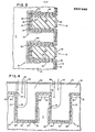
- Fig. 1 a plan view of an array of memory cells of the present invention.
- the array includes four memory cells 10, 12, 14 and 16 formed in trenches 18, 20, 22 and 24, respectively, located in a P type conductivity semiconductor substrate 26, as indicated also in the sectional views in Figs. 2 and 3 of the drawings.
- Each of the cells 10, 12, 14 and 16 includes a first N+ diffusion region 28 disposed in the semiconductor substrate 26 at the bottcm and along the lower portions of the sidewalls of the trenches 18, 20, 22 and 24.
- the first N+ diffusion region 28 acts as a storage node and serves as a first plate of a storage capacitor 30.
- a second N+ diffusion region 32 is disposed at the surface of the semiconductor substrate 26 adjacent to each of the trenches 18, 20, 22 and 24.
- the second N+ diffusion regions 32 are arranged in parallel, illustrated vertically in Fig. 1, to serve as bit/sense lines 32 for the array with each of the lines 32 associated with the cells of one column of the array.
- a first layer of silicon dioxide 34 is grown within the trenches 18, 20, 22 and 24 and over the second N+ diffusion regions 32, with the layer 34 being thicker over regions 32 due to the higher oxidation rate in the presence of the high N+ doping.
- a first layer of doped polysilicon 36 is deposited over the first layer of silicon dioxide 34 within the trenches 18, 20, 22 and 24 and over the surface of the substrate 26.
- the first layer of doped polysilicon 36 serves as a second plate of the storage capacitor 30 and as a field shield between the storage capacitors 30 and the bit/sense lines 32 of each of the memory cells.
- An opening 38 is formed in the first layer of polysilicon 36 on one sidewall of each of the trenches 18, 20, 22 and 24 between the bit/sense line 32 and the adjacent edge of the first N + diffusion region 28.
- a second layer of silicon dioxide 40 is grown over the remaining portions of the polysilicon layer 36.
- a second layer of doped polysilicon 42 is deposited over the second layer of silicon dioxide 40 and over the first layer of silicon dioxide 34 within the opening 38.
- the second polysilicon layer 42 serves as the control or gate electrode of a switch or field effect transistor 44 which includes first and second N+ diffusion regions 28 and 32 acting as source/drain electrodes.
- the trenches 18, 20, 22 and 24 may now be completely filled with any suitable material such as polyimide 46.
- Conductive lines 48 which may be made of copper doped aluminum, are arranged in parallel, illustrated horizontally in Fig. 1, so that each of the lines 48 contacts the gate electrodes 42 of one row of cells of the array to act as a word line.
- a very dense array of cells is formed with each of the cells having a large storage capacitor within a trench along with a switching device and a field shield which prevents current or charge leakage between adjacent cells when an appropriate voltage is applied to the first polysilicon layer 36.
- the cells 10, 12, 14 and 16 of the array of the present invention may be fabricated by any known process.
- the N+ bit/sense line diffusion region 32 can be formed by defining a chemical vapor deposition (CVD) arsenic doped oxide layer into strips with a subsequent thermal drive in of the arsenic doping into the silicon substrate 26.
- a second CVD undoped oxide layer can be defined in strips 'running orthogonal to the doped oxide strips. The intersection of these orthogonal strips can then be used as a mask for etching the trenches 18, 20, 22 and 24 that are self aligned to the bit/sense line diffusion regions 32.
- the CVD oxide layers may subsequently be removed, or left in place to reduce bit/sense line capacitance.
- the trenches 18, 20, 22 and 24 may be formed by using reactive ion etching techniques and may be 5 microns deep with an opening of 1.5 x 1.5 microns or 2.25 square microns.
- the N+ diffusion regions 28 may be made by chemically vapor depositing a thin layer of doped silicon dioxide within the trenches, filling the trenches with any suitable material such as a photoresist to a desired level, e. g,, as taught in commonly assigned U. S. Patent 4,295,924, filed December 17, 1979, by R. R. Garnache and D. M. Kenney, and issued on October 20, 1981, and then etching the unwanted upper portions of the doped silicon dioxide.
- the dopant e.g., arsenic
- the doped silicon dioxide is outdiffused into the bottom and sidewalls of the trenches to form the N+ diffusion regions 28.
- the opening 38 within the first polysilicon layer 34 after depositing the first polysilicon layer 34, the trenches 18, 20, 22 and 24 are filled with any suitable photoresist 50, as indicated in Fig. 4 of the drawings, and, with the use of an appropriate mask 52 having openings 54, wells 56 are formed in the photoresist 50 by using known reactive ion etching techniques.
- the mask 52 may be any known multilevel or multilayer photoresist mask having a non-erodable layer, e. g., polysilicon.
- an appropriate wet etchant such as HN0 3 /HF, or a freon dry plasma etchant, may be used to form the openings 38 within the first polysilicon layer 36.
- the first layer of polysilicon 34 may be continuous throughout the array, except for the openings 38, it should be understood that the second layer of polysilicon 42 must be appropriately etched into strips so that adjacent word lines 48 do not contact each other.
- the P type doping between and below these nodes 28 should be about 5 x 16 16 to 1 x 10 17 atoms/cm of boron.
- the substrate 26 may have an N type conductivity with the diffusion regions 28 and 32 being of a P+ type conductivity without departing from the spirit of this invention.
- dual oxide/nitride layers may be used where the silicon dioxide layers are indicated.
Landscapes
- Engineering & Computer Science (AREA)
- Manufacturing & Machinery (AREA)
- Physics & Mathematics (AREA)
- Condensed Matter Physics & Semiconductors (AREA)
- General Physics & Mathematics (AREA)
- Computer Hardware Design (AREA)
- Microelectronics & Electronic Packaging (AREA)
- Power Engineering (AREA)
- Semiconductor Memories (AREA)
- Semiconductor Integrated Circuits (AREA)
- Peptides Or Proteins (AREA)
Abstract
Description
- This invention relates to integrated semiconductor memory circuits and more particularly to a memory with a high density of cells, each of which employs a capacitor for storing a binary digit of information.
- Integrated semiconductor memory circuits, particularly those employing cells which include essentially a storage capacitor and a switch have achieved high memory cell densities. One of the simplest circuits for providing a small dynamic memory cell is described in commonly assigned U.S. Patent No. 3,387,286, filed July 14, 1967, by R.H. Dennard. Each cell employs a storage capacitor and a field effect transistor acting as a switch to selectively connect the capacitor to a bit/sense line.
- In also commonly assigned U.S. Patents Nos. 3,811,076 by W.M. Smith, and 3,841,926, by R.A. Garnache and W.M. Smith, both filed on January 2, 1973, there is disclosed a one device field effect transistor memory cell of the type described in the hereinabove identified Dennard patent which utilizes a layer of doped polysilicon and an N+ diffusion region in a P type conductivity semiconductor substrate separated by a dielectric medium disposed on the surface of the semiconductor substrate for forming the storage capacitor of the cell. The polysilicon layer extends beyond the storage capacitor to act as a field shield between adjacent cells by applying a negative bias or fixed negative potential to the polysilicon layer. The N+ diffusion region of the storage capacitor is formed by using a doped segment of an insulating layer disposed on the surface of the semiconductor substrate and outdiffusing the dopant into the substrate.
- In IBM Technical Disclosure Bulletin, Vol. 21, No. 9, February 1979, pp. 3823-3825, there is disclosed a one device memory cell which advantageously uses two layers of polysilicon.
- Although the cells described hereinabove do provide memories having a high density of cells in a planar or two dimensional arrangement, yet each cell does require a significant given area of semiconductor surface. To reduce the size of the given area for each cell, structures have been made wherein the cell is formed in a three dimensional arrangement, such as described in commonly assigned U.S. Patent No. 4,335,450, filed on January 30, 1980, by D.R. Thomas, wherein there is disclosed a cell having a transistor disposed on a sidewall of a groove or trench with the storage node disposed below the transistor.
- Also, commonly assigned U.S. Patent No. 4,397,075, filed on July 3, 1980, by J.J. Fatula, Jr. and P.L. Garbarino, and commonly assigned U.S. Patent Application having Serial No. 182,724, filed on August 29, 1980, by S.A. Abbas and R.C. Dockerty, describe a dense, vertical cell having the storage capacitor in a well or trench. Somewhat similar cells are disclosed in U.S. Patent No. 4,327,476, filed on December 7, 1979, and in IBM Technical Disclosure Bulletins, February 1975, by G.V. Clarke and J.E. Tomko, pp. 2579-2580, July 1982, by C.G. Jambotkar, pp. 593-596, and February 1984, by B. El-Kareh, R.R. Garnache and F.R. White, pp. 4699-4701.
- Furthermore, commonly assigned U.S. Patent No. a 4,462,040, filed on May 7, 1979, by I.T. Ho and J. Riseman discloses a one device dynamic random access memory utilizing a trench having vertical sidewalls with the storage capacitor and the transfer device located within the trench, and U.S. Patents No. 4,271,418, filed October 29, 1979, and 4,225,945, filed October 29, 1979, teach a one device memory cell formed in a groove or trench with the storage node located at the bottom of the trench, the bit/sense line at the top of this substrate and the transfer device on the sidewall of the trench.
- It is the object of this invention to provide a memory cell, in a three dimensional arrangement including a groove or trench, requiring a very small area of the surface of a semiconductor substrate, which has a high storage capacity and means disposed within the groove or trench for isolating adjacent cells.
- In accordance with the teachings of this invention, a memory cell, formed in a groove or trench, in a semiconductor substrate is provided which includes a storage capacitor located at the bottom of the trench, a bit/sense line disposed at the surface of the substrate, a transfer device located on the sidewall of the trench between the capacitor and the bit/sense line and a field shield for electrically isolating the storage capacitor.
- A significant density advance has been made in fast dynamic random access memories wherein, with presently known technology, memory chips each of which may have millions of cells formed therein, although for purposes of clarity only four are illustrated in the drawings, can be manufactured. Furthermore, each of these cells, which has an area of only four square or four features, is capable of storing a binary digit of information in a relatively large storage capacitor, thus, extremely sensitive sense amplifiers for detecting the stored signals in this very dense memory are not required. The vertical structure and arrangement of the cell elements within the trench provides a storage node capacitance which is relatively independent of cell area at the surface of the semiconductor substrate while electrically isolated from other cell elements resulting in a memory with improved density, signal strength and performance.
- The foregoing and other objects, features and advantages of the invention will be apparent form the following and more particular description of the preferred embodiments of the invention, as illustrated in the accompanying drawings.
-
- Fig. 1 is a plan view of an array of memory cells of the present invention,
- Fig. 2 is a sectional view of the array of cells illustrated in Fig. 1 of the drawings taken along line 2-2,
- Fig. 3 is a sectional view of the array of cells illustrated in Fig. 1 of the drawings taken along line 3-3, and
- Fig. 4 is a sectional view similar to that of Fig. 2 but taken at an early step during the making of the array.
- Referring to the drawings in more detail, there is illustrated in Fig. 1 a plan view of an array of memory cells of the present invention. The array includes four
memory cells trenches conductivity semiconductor substrate 26, as indicated also in the sectional views in Figs. 2 and 3 of the drawings. Each of thecells N+ diffusion region 28 disposed in thesemiconductor substrate 26 at the bottcm and along the lower portions of the sidewalls of thetrenches N+ diffusion region 28 acts as a storage node and serves as a first plate of astorage capacitor 30. A secondN+ diffusion region 32 is disposed at the surface of thesemiconductor substrate 26 adjacent to each of thetrenches N+ diffusion regions 32 are arranged in parallel, illustrated vertically in Fig. 1, to serve as bit/sense lines 32 for the array with each of thelines 32 associated with the cells of one column of the array. A first layer ofsilicon dioxide 34 is grown within thetrenches N+ diffusion regions 32, with thelayer 34 being thicker overregions 32 due to the higher oxidation rate in the presence of the high N+ doping. - A first layer of
doped polysilicon 36 is deposited over the first layer ofsilicon dioxide 34 within thetrenches substrate 26. The first layer ofdoped polysilicon 36 serves as a second plate of thestorage capacitor 30 and as a field shield between thestorage capacitors 30 and the bit/sense lines 32 of each of the memory cells. Anopening 38, as indicated in Fig. 2 of the drawings, is formed in the first layer ofpolysilicon 36 on one sidewall of each of thetrenches sense line 32 and the adjacent edge of the first N+diffusion region 28. A second layer ofsilicon dioxide 40 is grown over the remaining portions of thepolysilicon layer 36. A second layer ofdoped polysilicon 42 is deposited over the second layer ofsilicon dioxide 40 and over the first layer ofsilicon dioxide 34 within theopening 38. Thesecond polysilicon layer 42 serves as the control or gate electrode of a switch orfield effect transistor 44 which includes first and secondN+ diffusion regions trenches polyimide 46. -
Conductive lines 48, which may be made of copper doped aluminum, are arranged in parallel, illustrated horizontally in Fig. 1, so that each of thelines 48 contacts thegate electrodes 42 of one row of cells of the array to act as a word line. - It can be seen from the teachings of this invention that a very dense array of cells is formed with each of the cells having a large storage capacitor within a trench along with a switching device and a field shield which prevents current or charge leakage between adjacent cells when an appropriate voltage is applied to the
first polysilicon layer 36. - Writing data into and reading from the memory array illustrated in Figs. 1-3 of the drawings is preformed in a manner similar to that described in the prior art, e.g.', in the hereinabove cited Dennard patent.
- The
cells line diffusion region 32 can be formed by defining a chemical vapor deposition (CVD) arsenic doped oxide layer into strips with a subsequent thermal drive in of the arsenic doping into thesilicon substrate 26. A second CVD undoped oxide layer can be defined in strips 'running orthogonal to the doped oxide strips. The intersection of these orthogonal strips can then be used as a mask for etching thetrenches line diffusion regions 32. The CVD oxide layers may subsequently be removed, or left in place to reduce bit/sense line capacitance. Thetrenches N+ diffusion regions 28 may be made by chemically vapor depositing a thin layer of doped silicon dioxide within the trenches, filling the trenches with any suitable material such as a photoresist to a desired level, e. g,, as taught in commonly assigned U. S. Patent 4,295,924, filed December 17, 1979, by R. R. Garnache and D. M. Kenney, and issued on October 20, 1981, and then etching the unwanted upper portions of the doped silicon dioxide. After removing the unwanted material from the trench, which defines the desired level of doped silicon dioxide within the trench, the dopant, e.g., arsenic, within the doped silicon dioxide is outdiffused into the bottom and sidewalls of the trenches to form theN+ diffusion regions 28. Furthermore, to form theopening 38 within thefirst polysilicon layer 34, after depositing thefirst polysilicon layer 34, thetrenches suitable photoresist 50, as indicated in Fig. 4 of the drawings, and, with the use of anappropriate mask 52 havingopenings 54,wells 56 are formed in thephotoresist 50 by using known reactive ion etching techniques. Themask 52 may be any known multilevel or multilayer photoresist mask having a non-erodable layer, e. g., polysilicon. After thewells 56 are formed in thephotoresist 50, an appropriate wet etchant, such as HN03/HF, or a freon dry plasma etchant, may be used to form theopenings 38 within thefirst polysilicon layer 36. - Although the first layer of
polysilicon 34 may be continuous throughout the array, except for theopenings 38, it should be understood that the second layer ofpolysilicon 42 must be appropriately etched into strips so thatadjacent word lines 48 do not contact each other. To prevent storage node to storage node punch-through the P type doping between and below thesenodes 28 should be about 5 x 1616 to 1 x 10¹⁷ atoms/cm of boron. Also, if desired, thesubstrate 26 may have an N type conductivity with thediffusion regions - While the invention has been particularly shown and described with reference to preferred embodiments thereof, it will be understood by those skilled in the art that various changes in form and details may be made therein without departing from the spirit and scope of the invention.
- What is claimed is:
Claims (17)
Priority Applications (1)
| Application Number | Priority Date | Filing Date | Title |
|---|---|---|---|
| AT86113867T ATE99456T1 (en) | 1985-10-31 | 1986-10-07 | HIGH DENSITY STORAGE. |
Applications Claiming Priority (2)
| Application Number | Priority Date | Filing Date | Title |
|---|---|---|---|
| US06/793,401 US4751558A (en) | 1985-10-31 | 1985-10-31 | High density memory with field shield |
| US793401 | 1985-10-31 |
Publications (3)
| Publication Number | Publication Date |
|---|---|
| EP0221380A2 true EP0221380A2 (en) | 1987-05-13 |
| EP0221380A3 EP0221380A3 (en) | 1989-06-28 |
| EP0221380B1 EP0221380B1 (en) | 1993-12-29 |
Family
ID=25159840
Family Applications (1)
| Application Number | Title | Priority Date | Filing Date |
|---|---|---|---|
| EP86113867A Expired - Lifetime EP0221380B1 (en) | 1985-10-31 | 1986-10-07 | High density memory |
Country Status (8)
| Country | Link |
|---|---|
| US (1) | US4751558A (en) |
| EP (1) | EP0221380B1 (en) |
| JP (1) | JPS62105466A (en) |
| AT (1) | ATE99456T1 (en) |
| AU (1) | AU580450B2 (en) |
| BR (1) | BR8604548A (en) |
| CA (1) | CA1248231A (en) |
| DE (1) | DE3689467T2 (en) |
Cited By (3)
| Publication number | Priority date | Publication date | Assignee | Title |
|---|---|---|---|---|
| EP0325257A1 (en) * | 1988-01-21 | 1989-07-26 | Fujitsu Limited | Semiconductor device having a trench and a method for producing the same |
| US4970580A (en) * | 1987-11-28 | 1990-11-13 | Mitsubishi Denki Kabushiki Kaisha | Semiconductor memory device having protruding cell configuration |
| GB2238909A (en) * | 1989-12-08 | 1991-06-12 | Samsung Electronics Co Ltd | Capacitors for DRAM cells |
Families Citing this family (39)
| Publication number | Priority date | Publication date | Assignee | Title |
|---|---|---|---|---|
| USRE33261E (en) * | 1984-07-03 | 1990-07-10 | Texas Instruments, Incorporated | Trench capacitor for high density dynamic RAM |
| US5208657A (en) * | 1984-08-31 | 1993-05-04 | Texas Instruments Incorporated | DRAM Cell with trench capacitor and vertical channel in substrate |
| US4824793A (en) * | 1984-09-27 | 1989-04-25 | Texas Instruments Incorporated | Method of making DRAM cell with trench capacitor |
| US5102817A (en) * | 1985-03-21 | 1992-04-07 | Texas Instruments Incorporated | Vertical DRAM cell and method |
| US5164917A (en) * | 1985-06-26 | 1992-11-17 | Texas Instruments Incorporated | Vertical one-transistor DRAM with enhanced capacitance and process for fabricating |
| USRE33972E (en) * | 1986-07-15 | 1992-06-23 | International Business Machines Corporation | Two square memory cells |
| US4949151A (en) * | 1986-09-24 | 1990-08-14 | Hitachi, Ltd. | Bipolar transistor having side wall base and collector contacts |
| US4829017A (en) * | 1986-09-25 | 1989-05-09 | Texas Instruments Incorporated | Method for lubricating a high capacity dram cell |
| US4916524A (en) * | 1987-03-16 | 1990-04-10 | Texas Instruments Incorporated | Dram cell and method |
| JPH0810757B2 (en) * | 1987-05-25 | 1996-01-31 | 松下電子工業株式会社 | Method for manufacturing semiconductor device |
| DE3851102D1 (en) * | 1987-07-10 | 1994-09-22 | Siemens Ag | Highly integrable memory cell and method for its production. |
| US5109259A (en) * | 1987-09-22 | 1992-04-28 | Texas Instruments Incorporated | Multiple DRAM cells in a trench |
| JPH01132176A (en) * | 1987-11-18 | 1989-05-24 | Canon Inc | Optoelectric conversion device |
| US5014099A (en) * | 1988-05-26 | 1991-05-07 | Texas Instruments Incorporated | Dynamic RAM cell with trench capacitor and trench transistor |
| US5106776A (en) * | 1988-06-01 | 1992-04-21 | Texas Instruments Incorporated | Method of making high performance composed pillar dRAM cell |
| US5103276A (en) * | 1988-06-01 | 1992-04-07 | Texas Instruments Incorporated | High performance composed pillar dram cell |
| US5225363A (en) * | 1988-06-28 | 1993-07-06 | Texas Instruments Incorporated | Trench capacitor DRAM cell and method of manufacture |
| US5105245A (en) * | 1988-06-28 | 1992-04-14 | Texas Instruments Incorporated | Trench capacitor DRAM cell with diffused bit lines adjacent to a trench |
| US4958206A (en) * | 1988-06-28 | 1990-09-18 | Texas Instruments Incorporated | Diffused bit line trench capacitor dram cell |
| US5422294A (en) * | 1993-05-03 | 1995-06-06 | Noble, Jr.; Wendell P. | Method of making a trench capacitor field shield with sidewall contact |
| JPH08250677A (en) * | 1994-12-28 | 1996-09-27 | Nippon Steel Corp | Semiconductor memory device and its fabrication method |
| US6222254B1 (en) * | 1997-03-31 | 2001-04-24 | Intel Corporation | Thermal conducting trench in a semiconductor structure and method for forming the same |
| US7067406B2 (en) * | 1997-03-31 | 2006-06-27 | Intel Corporation | Thermal conducting trench in a semiconductor structure and method for forming the same |
| JP4609985B2 (en) * | 2004-06-30 | 2011-01-12 | ルネサスエレクトロニクス株式会社 | Semiconductor chip, method for manufacturing the same, and semiconductor device |
| US7518179B2 (en) | 2004-10-08 | 2009-04-14 | Freescale Semiconductor, Inc. | Virtual ground memory array and method therefor |
| US7642594B2 (en) * | 2005-07-25 | 2010-01-05 | Freescale Semiconductor, Inc | Electronic device including gate lines, bit lines, or a combination thereof |
| US7619275B2 (en) * | 2005-07-25 | 2009-11-17 | Freescale Semiconductor, Inc. | Process for forming an electronic device including discontinuous storage elements |
| US7285819B2 (en) * | 2005-07-25 | 2007-10-23 | Freescale Semiconductor, Inc. | Nonvolatile storage array with continuous control gate employing hot carrier injection programming |
| US7112490B1 (en) * | 2005-07-25 | 2006-09-26 | Freescale Semiconductor, Inc. | Hot carrier injection programmable structure including discontinuous storage elements and spacer control gates in a trench |
| US20070020840A1 (en) * | 2005-07-25 | 2007-01-25 | Freescale Semiconductor, Inc. | Programmable structure including nanocrystal storage elements in a trench |
| US7262997B2 (en) * | 2005-07-25 | 2007-08-28 | Freescale Semiconductor, Inc. | Process for operating an electronic device including a memory array and conductive lines |
| US7582929B2 (en) * | 2005-07-25 | 2009-09-01 | Freescale Semiconductor, Inc | Electronic device including discontinuous storage elements |
| US7619270B2 (en) * | 2005-07-25 | 2009-11-17 | Freescale Semiconductor, Inc. | Electronic device including discontinuous storage elements |
| US7314798B2 (en) * | 2005-07-25 | 2008-01-01 | Freescale Semiconductor, Inc. | Method of fabricating a nonvolatile storage array with continuous control gate employing hot carrier injection programming |
| US7394686B2 (en) * | 2005-07-25 | 2008-07-01 | Freescale Semiconductor, Inc. | Programmable structure including discontinuous storage elements and spacer control gates in a trench |
| US7592224B2 (en) | 2006-03-30 | 2009-09-22 | Freescale Semiconductor, Inc | Method of fabricating a storage device including decontinuous storage elements within and between trenches |
| US7651916B2 (en) * | 2007-01-24 | 2010-01-26 | Freescale Semiconductor, Inc | Electronic device including trenches and discontinuous storage elements and processes of forming and using the same |
| US7838922B2 (en) * | 2007-01-24 | 2010-11-23 | Freescale Semiconductor, Inc. | Electronic device including trenches and discontinuous storage elements |
| US7572699B2 (en) * | 2007-01-24 | 2009-08-11 | Freescale Semiconductor, Inc | Process of forming an electronic device including fins and discontinuous storage elements |
Citations (2)
| Publication number | Priority date | Publication date | Assignee | Title |
|---|---|---|---|---|
| US3841926A (en) * | 1973-01-02 | 1974-10-15 | Ibm | Integrated circuit fabrication process |
| EP0042084A1 (en) * | 1980-06-12 | 1981-12-23 | International Business Machines Corporation | Semiconductor device especially a memory cell in V-MOS technology |
Family Cites Families (16)
| Publication number | Priority date | Publication date | Assignee | Title |
|---|---|---|---|---|
| US3387286A (en) * | 1967-07-14 | 1968-06-04 | Ibm | Field-effect transistor memory |
| US3811076A (en) * | 1973-01-02 | 1974-05-14 | Ibm | Field effect transistor integrated circuit and memory |
| US4225945A (en) * | 1976-01-12 | 1980-09-30 | Texas Instruments Incorporated | Random access MOS memory cell using double level polysilicon |
| JPS55141750A (en) * | 1979-04-23 | 1980-11-05 | Nec Corp | Insulated gate type semiconductor device |
| US4462040A (en) * | 1979-05-07 | 1984-07-24 | International Business Machines Corporation | Single electrode U-MOSFET random access memory |
| US4271418A (en) * | 1979-10-29 | 1981-06-02 | American Microsystems, Inc. | VMOS Memory cell and method for making same |
| JPS5681968A (en) * | 1979-12-07 | 1981-07-04 | Toshiba Corp | Manufacture of semiconductor device |
| US4335450A (en) * | 1980-01-30 | 1982-06-15 | International Business Machines Corporation | Non-destructive read out field effect transistor memory cell system |
| US4397075A (en) * | 1980-07-03 | 1983-08-09 | International Business Machines Corporation | FET Memory cell structure and process |
| JPS58213464A (en) * | 1982-06-04 | 1983-12-12 | Nec Corp | Semiconductor device |
| JPS5982761A (en) * | 1982-11-04 | 1984-05-12 | Hitachi Ltd | Semiconductor memory |
| JPS60136369A (en) * | 1983-12-26 | 1985-07-19 | Toshiba Corp | Manufacture of semiconductor device |
| JPH0648719B2 (en) * | 1984-01-20 | 1994-06-22 | 株式会社日立製作所 | Semiconductor memory device |
| JPS60206163A (en) * | 1984-03-30 | 1985-10-17 | Toshiba Corp | Semiconductor memory device |
| US4672410A (en) * | 1984-07-12 | 1987-06-09 | Nippon Telegraph & Telephone | Semiconductor memory device with trench surrounding each memory cell |
| US4769786A (en) * | 1986-07-15 | 1988-09-06 | International Business Machines Corporation | Two square memory cells |
-
1985
- 1985-10-31 US US06/793,401 patent/US4751558A/en not_active Expired - Lifetime
-
1986
- 1986-08-20 JP JP61193002A patent/JPS62105466A/en active Granted
- 1986-08-28 CA CA000517130A patent/CA1248231A/en not_active Expired
- 1986-09-23 BR BR8604548A patent/BR8604548A/en not_active IP Right Cessation
- 1986-09-23 AU AU63072/86A patent/AU580450B2/en not_active Ceased
- 1986-10-07 DE DE3689467T patent/DE3689467T2/en not_active Expired - Fee Related
- 1986-10-07 AT AT86113867T patent/ATE99456T1/en not_active IP Right Cessation
- 1986-10-07 EP EP86113867A patent/EP0221380B1/en not_active Expired - Lifetime
Patent Citations (2)
| Publication number | Priority date | Publication date | Assignee | Title |
|---|---|---|---|---|
| US3841926A (en) * | 1973-01-02 | 1974-10-15 | Ibm | Integrated circuit fabrication process |
| EP0042084A1 (en) * | 1980-06-12 | 1981-12-23 | International Business Machines Corporation | Semiconductor device especially a memory cell in V-MOS technology |
Cited By (4)
| Publication number | Priority date | Publication date | Assignee | Title |
|---|---|---|---|---|
| US4970580A (en) * | 1987-11-28 | 1990-11-13 | Mitsubishi Denki Kabushiki Kaisha | Semiconductor memory device having protruding cell configuration |
| EP0325257A1 (en) * | 1988-01-21 | 1989-07-26 | Fujitsu Limited | Semiconductor device having a trench and a method for producing the same |
| US4987470A (en) * | 1988-01-21 | 1991-01-22 | Fujitsu Limited | Semiconductor dram device having a trench |
| GB2238909A (en) * | 1989-12-08 | 1991-06-12 | Samsung Electronics Co Ltd | Capacitors for DRAM cells |
Also Published As
| Publication number | Publication date |
|---|---|
| JPS62105466A (en) | 1987-05-15 |
| BR8604548A (en) | 1987-05-26 |
| EP0221380B1 (en) | 1993-12-29 |
| JPH0582988B2 (en) | 1993-11-24 |
| DE3689467D1 (en) | 1994-02-10 |
| CA1248231A (en) | 1989-01-03 |
| ATE99456T1 (en) | 1994-01-15 |
| DE3689467T2 (en) | 1994-06-23 |
| AU580450B2 (en) | 1989-01-12 |
| AU6307286A (en) | 1987-05-07 |
| EP0221380A3 (en) | 1989-06-28 |
| US4751558A (en) | 1988-06-14 |
Similar Documents
| Publication | Publication Date | Title |
|---|---|---|
| US4751558A (en) | High density memory with field shield | |
| US4801988A (en) | Semiconductor trench capacitor cell with merged isolation and node trench construction | |
| US5574299A (en) | Semiconductor device having vertical conduction transistors and cylindrical cell gates | |
| US5191509A (en) | Textured polysilicon stacked trench capacitor | |
| US5017981A (en) | Semiconductor memory and method for fabricating the same | |
| US5021842A (en) | Trench DRAM cell with different insulator thicknesses | |
| US5138411A (en) | Anodized polysilicon layer lower capacitor plate of a dram to increase capacitance | |
| EP0254046B1 (en) | Semiconductor memory | |
| US4791463A (en) | Structure for contacting devices in three dimensional circuitry | |
| US4811067A (en) | High density vertically structured memory | |
| US5482885A (en) | Method for forming most capacitor using poly spacer technique | |
| US4896197A (en) | Semiconductor memory device having trench and stacked polysilicon storage capacitors | |
| US6815734B1 (en) | Varied trench depth for thyristor isolation | |
| KR910007111B1 (en) | Semiconductor memory device and its method for manufacturing | |
| US5940714A (en) | Method of fabricating a capacitor electrode structure in integrated circuit through self-aligned process | |
| US5539230A (en) | Chimney capacitor | |
| US7049182B1 (en) | Shunt connection to the emitter of a thyristor | |
| US6069819A (en) | Variable threshold voltage DRAM cell | |
| US5258321A (en) | Manufacturing method for semiconductor memory device having stacked trench capacitors and improved intercell isolation | |
| US5512768A (en) | Capacitor for use in DRAM cell using surface oxidized silicon nodules | |
| EP0392156B1 (en) | Semiconductor memory with high cell density | |
| US5146425A (en) | Mist type dynamic random access memory cell and formation process thereof | |
| US6238974B1 (en) | Method of forming DRAM capacitors with a native oxide etch-stop | |
| JPH11154737A (en) | Dram cell and manufacture of dram cell | |
| US5109259A (en) | Multiple DRAM cells in a trench |
Legal Events
| Date | Code | Title | Description |
|---|---|---|---|
| PUAI | Public reference made under article 153(3) epc to a published international application that has entered the european phase |
Free format text: ORIGINAL CODE: 0009012 |
|
| AK | Designated contracting states |
Kind code of ref document: A2 Designated state(s): AT DE FR GB |
|
| 17P | Request for examination filed |
Effective date: 19870821 |
|
| PUAL | Search report despatched |
Free format text: ORIGINAL CODE: 0009013 |
|
| AK | Designated contracting states |
Kind code of ref document: A3 Designated state(s): AT DE FR GB |
|
| 17Q | First examination report despatched |
Effective date: 19910528 |
|
| GRAA | (expected) grant |
Free format text: ORIGINAL CODE: 0009210 |
|
| AK | Designated contracting states |
Kind code of ref document: B1 Designated state(s): AT DE FR GB |
|
| REF | Corresponds to: |
Ref document number: 99456 Country of ref document: AT Date of ref document: 19940115 Kind code of ref document: T |
|
| REF | Corresponds to: |
Ref document number: 3689467 Country of ref document: DE Date of ref document: 19940210 |
|
| ET | Fr: translation filed | ||
| PLBE | No opposition filed within time limit |
Free format text: ORIGINAL CODE: 0009261 |
|
| STAA | Information on the status of an ep patent application or granted ep patent |
Free format text: STATUS: NO OPPOSITION FILED WITHIN TIME LIMIT |
|
| 26N | No opposition filed | ||
| PGFP | Annual fee paid to national office [announced via postgrant information from national office to epo] |
Ref country code: AT Payment date: 19950825 Year of fee payment: 10 |
|
| PGFP | Annual fee paid to national office [announced via postgrant information from national office to epo] |
Ref country code: DE Payment date: 19951030 Year of fee payment: 10 |
|
| PG25 | Lapsed in a contracting state [announced via postgrant information from national office to epo] |
Ref country code: AT Effective date: 19961007 |
|
| PGFP | Annual fee paid to national office [announced via postgrant information from national office to epo] |
Ref country code: FR Payment date: 19961007 Year of fee payment: 11 |
|
| PG25 | Lapsed in a contracting state [announced via postgrant information from national office to epo] |
Ref country code: DE Effective date: 19970701 |
|
| PG25 | Lapsed in a contracting state [announced via postgrant information from national office to epo] |
Ref country code: FR Free format text: THE PATENT HAS BEEN ANNULLED BY A DECISION OF A NATIONAL AUTHORITY Effective date: 19971031 |
|
| REG | Reference to a national code |
Ref country code: FR Ref legal event code: ST |
|
| PGFP | Annual fee paid to national office [announced via postgrant information from national office to epo] |
Ref country code: GB Payment date: 19990930 Year of fee payment: 14 |
|
| PG25 | Lapsed in a contracting state [announced via postgrant information from national office to epo] |
Ref country code: GB Free format text: LAPSE BECAUSE OF NON-PAYMENT OF DUE FEES Effective date: 20001007 |
|
| GBPC | Gb: european patent ceased through non-payment of renewal fee |
Effective date: 20001007 |