EP0217647A2 - Time base correction of television signals - Google Patents
Time base correction of television signals Download PDFInfo
- Publication number
- EP0217647A2 EP0217647A2 EP86307401A EP86307401A EP0217647A2 EP 0217647 A2 EP0217647 A2 EP 0217647A2 EP 86307401 A EP86307401 A EP 86307401A EP 86307401 A EP86307401 A EP 86307401A EP 0217647 A2 EP0217647 A2 EP 0217647A2
- Authority
- EP
- European Patent Office
- Prior art keywords
- phase
- frequency
- signal
- burst
- clock
- Prior art date
- Legal status (The legal status is an assumption and is not a legal conclusion. Google has not performed a legal analysis and makes no representation as to the accuracy of the status listed.)
- Granted
Links
Images


Classifications
-
- H—ELECTRICITY
- H04—ELECTRIC COMMUNICATION TECHNIQUE
- H04N—PICTORIAL COMMUNICATION, e.g. TELEVISION
- H04N9/00—Details of colour television systems
- H04N9/79—Processing of colour television signals in connection with recording
- H04N9/87—Regeneration of colour television signals
- H04N9/89—Time-base error compensation
- H04N9/896—Time-base error compensation using a digital memory with independent write-in and read-out clock generators
Definitions
- This invention relates to a time base correction system and is particular to a system that employs digital circuitry for measuring and correcting frequency and phase errors of a recorded color television signal during playback.
- phase locked loop including a voltage controlled oscillator (VCO) to measure the difference in phase and frequency between the VCO clock frequency and the burst signal component of the composite color television signal.
- VCO voltage controlled oscillator
- phase locked loops used in prior art systems do not operate sufficiently fast to follow the rapid changes in the frequency and phase of a video signal recorded on, for example, a fast moving tape.
- the invention overcomes the above disadvantages while providing various added advantages over present schemes for correcting frequency and phase errors.
- the invention provides an improved time base correction system employing digital circuitry in which adjustments for frequency and phase errors are minimized. Further, the invention provides a time base correction system that may follow and correct frequency and phase errors relatively rapidly to avoid buildup of large errors.
- a sampling clock is used which has a precise and continuous relationship to the color subcarrier of the incoming video signal.
- the invention time base correction system provides phase correction of a color video signal which includes a color burst component by employing a clock signal preferably having a frequency that is a multiple of the subcarrier frequency.
- the clock signal is locked in phase to the color burst component of the video signal and phase correction is effectuated with reference to a digital sampled burst signal so that any errors in the analog portion of the video signal are servoed to zero in a closed loop arrangement.
- a time base correction system converts components of an off-tape analog video signal to digital pulses.
- the digitized sync and burst components of the video signal are filtered and processed in a high speed digital signal processor to generate a frequency control word.
- a digital frequency synthesizer generates a clock signal at subcarrier frequency in response to the frequency control word, and the clock signal is applied to an analog-to-digital (A/D) converter which operates at four times the subcarrier frequency.
- A/D converter analog-to-digital converter which operates at four times the subcarrier frequency.
- the output of the A/D converter is a series of binary words at the multiplied frequency rate representing samples of successive portions of the video signal.
- the samples are fed back to the input of a closed feedback loop constituting sync and burst filters, a processor, synthesizer and phase locked loop.
- the clocked binary data samples of off-tape video signal are passed to a time base correction memory for further time base correction of the sampled video signal.
- a composite analog video signal is derived from a prerecorded magnetic tape and passed through a delay circuit 10 providing a delay of one horizontal line, i.e., 63.5 ⁇ sec. plus 3.5 ⁇ sec, or a total delay of approximately 67.0 ⁇ sec.
- This delay produces a "late video" signal and allows a look ahead at the phase of the burst signal at the beginning and at the end of each horizontal line to determine whether any changes in phase have occurred during the period of the horizontal line under consideration.
- a delay of more than one television line enables the video input to switch dynamically between the delayed burst signal and the burst of the undelayed signal, so that both burst signals are applied through a gated switch 12 to an analog-to-digital converter 14.
- the delayed analog signal is applied to the gated switch 12 which is normally in the "late video” position, but switches to "input video” or “early video” during the input video burst time.
- the output signal from the timed switch contains active video and burst components and the leading edge of the horizontal sync from the late video signal, as well as the burst component of the input or early video signal.
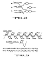
- the timing relationship of the early and late video signals and the combined signal obtained from the output circuit of the gated switch 12 are delineated in FIG. 2.
- the combined signal is passed to the analog-to-digital converter 14, which samples the video output signal from the switch 12 at four times the subcarrier frequency, digitized to nine-bit words.
- Each digital word having sync and burst is processed by the time base correction circuit of this invention to determine and compensate phase and frequency errors that occur between the input video and a 4f sc (4x subcarrier frequency) clock.
- the digitized signal containing the early burst and late burst components, is passed through a sync low pass filter 16 and a burst bandpass filter 18.
- the filter 18 averages about six cycles of each burst to reject chroma noise.
- the bandpass filter 18 For each burst, the bandpass filter 18 produces two filtered samples, designated as "A" and "B", which are 90° apart, as illustrated in FIG. 3. As shown in FIG. 3, the filtered samples A and B comprise the odd and even samples respectively, which are averaged about a baseline by adding the differences between each pair of samples in one complete cycle.
- the filtered burst samples A and B are applied to a high speed digital signal processor 20 which is illustrated in detail and will be described with reference to FIG. 4.
- the signal processor 20 calculates the sync and burst phase errors relative to the clock generated in a closed feedback loop, which includes the processor 20, a digital frequency synthesizer 22 that operates under control of a fixed reference clock or crystal oscillator 24, and an analog phase lock loop 26 operating at a frequency 4 times the subcarrier frequency f sc .
- the feedback clock signal is returned via lead 25 to the converter 14 and to the filters 16 and 18, and allows precise adjustment of frequency and phase of the digitizing clock.
- the burst samples A and B are used to develop a signal that represents the phase error between the signal obtained from the phase lock loop 26, which provides a four times subcarrier sampling clock (4f sc ) and the zero crossings of the off-tape burst signal.
- the burst samples are changed with relation to the clock phase error as depicted in FIG. 6.
- Sample A is negative when the clock is advanced in phase, and positive when the clock is delayed in phase.
- burst sample A is at zero, and burst sample B is displaced by 90°, as shown in FIG. 6c. Since sample A does not follow the phase error in a linear fashion, a clock to burst phase calculator 32, shown in FIG.
- the error signal ⁇ represents the phase error between the clock and burst over 360°, and is independent of burst amplitude. It is noted that ⁇ depends only on the ratio of sample A to sample B. The arctangent of the ratio of these two values define the sampling position of the burst. The arctangent of is valid only for ⁇ over the range of ⁇ 90°. To obtain phase error over the entire 360° range, the calculator 32 senses the sign of sample B and adds 180° to ⁇ if sample B is negative.
- the clock phase error value for the late burst is directed to a switch 64 which enables line-by-line phase correction of the clock by the frequency synthesizer.
- the clock-to-burst calculator 32 passes the phase error values from early burst to a burst phase subtractor including a register and subtractor circuit 36.
- the subtractor circuit gives the phase error across a line.
- the clock phase error across a line is then applied to a constant scaler 38, and an 40 which forms a frequency accumulator with register 42 that is timed by the horizontal clock pulse.
- the K scaler 38 converts the phase error across a line to frequency error.
- Velocity compensation is achieved by setting the clock subcarrier frequency to be equal to the offtape video subcarrier frequency at the start of each line
- the clock determines the frequency error between the input video and the clock by measuring the phase error that accumulates across a line relative to the current subcarrier clock.
- the phase error is obtained by comparing two consecutive bursts of the input video to the current clock. If no frequency error exists, the clock-to-burst phase measurement of one burst is the same as for the next burst.
- the burst phase subtractor 34, 36 serves to calculate the phase error across a line by subtracting the clock-to-burst phase values of the two consecutive bursts.
- the clock frequency error signal from the K scaler 38 represents the amount by which the frequency of the clock must be changed to match the input signal frequency.
- the current clock frequency value is maintained by the frequency accumulator, consisting of the adder 40 and shift register 42. For each horizontal line, the frequency error is added to the current subcarrier clock frequency to form a new clock frequency, which replaces the previous frequency value as the register 42 is clocked for each line.
- the frequency accumulator allows the clock to lock its frequency to that of the input signal in a closed loop configuration. If the clock is low in frequency, the frequency error will be positive and the current clock frequency will increase until the error is zero. Similarly, if the clock is high in frequency, the error will be negative and the clock frequency will decrease until the error is zero.
- the output of the frequency accumulator is a 20-bit frequency control word that is passed to the frequency synthesizer 22.
- the frequency synthesizer 22 which is the digital equivalent of a voltage controlled oscillator (VCO), operates to correct the phase of the 4x subcarrier clock on a line-by-line basis.
- the synthesizer includes a phase accumulator 43, consisting of an adder 44 and register 46, under control of the reference clock 24, which provides a fixed 20.46 MHz timing signal.
- the updated frequency control word from register 42 of the processor 20 is fed to the phase accumulator 43 of the frequency synthesizer 22.
- FIG. 8a illustrates the phase accumulator operating at the subcarrier frequency of 3.58 MHz. If using another format than the NTSC standard, for example the PAL or PAL-M formats, the phase accumulator is programmed for 4.43 MHz by choosing a larger phase increment.
- the phase accumulator generates a digital ramp (FIG. 8b) at the desired output frequency (f sc ).
- the phase accumulator which is clocked at a constant rate by the crystal oscillator 24, provides an output signal to register 46 of a 20-bit binary number representing 360° of phase.
- the phase advances by an amount equal to the value of the frequency control word.
- the phase continues to increase until it exceeds 360°. At this point, the accumulator overflows and the phase wraps around to a number less than 360°, derived from the current phase and the phase increment represented by the control word.
- phase increment or control word For example, if the current phase is 350° and the phase increment or control word is 27°, the accumulator overflows to 17°.
- the phase will cycle through 360° of range at a rate proportional to the phase increment or frequency control word.
- the frequency of the phase accumulator output signal is directly related to the value of the phase increment or the frequency control word.
- the digital ramp waveform generated by the phase accumulator is converted to a digital representation of a sine wave form by the sine lookup PROM 48.
- the PROM converts the digital signal from the phase accumulator to a sine wave amplitude, and functions to convert 360° of phase to one full sine wave cycle.
- the output signal from the sine PROM is a digital word that is converted by the digital-to-analog converter 50 to a series of voltage levels which represent the instantaneous amplitude of the sine wave, as depicted in FIG. 8b.
- the output from the digital-to-analog converter is sinusoidal, but contains sampling steps at the 20.46 MHz clock rate, which are removed by a low pass filter 52 with a 7 MHz cutoff frequency. The result is a pure fundamental sine wave having the correct frequency of 3.58 MHz, such as shown in FIG. 8c.
- phase lock loop 26 which conventionally contains a phase comparator, a loop filter, a voltage controlled oscillator (VCO), and a divide by 4 counter.
- the phase lock loop 26 settles rapidly to the line-by-line phase corrections that are applied to the tape subcarrier phase via switch 64 and thus has a very high bandwidth. Also, as a result, phase noise generated by the analog VCO is suppressed.
- the digital sync low pass filter 16 operates to average several adjacent video samples to form each output samplee, and is used in conjunction with burst to provide filtered chroma line type signals that are used by a memory control to maintain a correct color at the output of the timing base correction system.
- the digitized sync leading edge from late video which is applied to the filter 16 is utilized by the tape clock to generate horizontal timing signals.
- the digitized late video signal that is processed by the analog-to-digital converter 14 is applied to the digital sync low pass filter 16.
- the filtered signal is compared in a comparator 56 which generates coarse sliced sync signals that go high when the video sync samples cross below a predetermined slice level.
- the detected digitized sync leading edge signals are sampled at the 4f sc rate and accurate timing information is obtained by the clock-to-sync phase calculator 54.
- the phase between the sync slice crossing and the first clock sample below the slice level is computed by determining the phase ⁇ cs which is equal to 90° times (S-L)/(U-L), where S is the 50% slice level, U is the sample just above the slice level and L is the sample just below the slice level.
- the late video sync signal that is provided by the phase calulator 54 contains sync-to-burst phase information that is applied to an adder 56 which produces a measured sync-subcarrier phase (scH) of the offtape signal for each horizontal line.
- the measurement is defined over 360° and is nominally 0° for video lines with positive burst polarity and 180° for negative burst lines.
- a burst polarity signal H/2 (where H is at horizontal rate) is obtained for further utilization.
- the phase reference is set midway between the two scH values for positive and negative burst types to afford maximum immunity to noise.
- a horizontal write pulse is produced by means of a comparator 58 coupled to receive the filtered sync signal from the low pass filter 16.
- the comparator 58 provides a coarse sliced sync signal to a burst crossing selector 62, which produces an H write pulse timed to the burst zero crossing phase.
- the burst zero crossing is selected by generating a one cycle wide window timed to the 50% slice point of the leading edge of the late sync signals. This window is delayed from sync so that its center is coincident with burst zero crossings of a standard scH phase signal.
- the positive zero crossing closest to the center of the window is selected for timing if H/2 is low, i.e., a positive burst is present, while the negative zero crossing nearest the window center is selected if H/2 is high, when a negative burst is present.
- a time base correction circuit for use in a television signal video recording and playback system wherein a 4x subcarrier frequency digital clock is generated and locked in phase and frequency to the input video and burst signals derived off the recording tape.
- the clock follows the timing variations of the offtape signal over all speed ranges of the playback machine.
- the clock provides a horizontal timing pulse that is timed to a selected burst zero crossing of the offtape signal.
- the timing pulse is used by the timing correction circuit to define the start of each horizontal line stored in a memory. All timing error measurement is based on digitized sync and burst signals obtained from the analog-to-digital converter at the input to the correction circuitry, obviating the need for a separate analog phase comparator with associated circuitry.
Abstract
Description
- This invention relates to a time base correction system and is particular to a system that employs digital circuitry for measuring and correcting frequency and phase errors of a recorded color television signal during playback.
- In color television recording systems that employ NTSC signals including horizontal sync and color burst components, inter alia, it is usually necessary to correct the timing errors caused by variations in tape speed, for example, or for frequency and phase differences appearing in the signal that is recorded. In order to provide the desired correction, prior art video systems generally employ a phase locked loop (PLL) including a voltage controlled oscillator (VCO) to measure the difference in phase and frequency between the VCO clock frequency and the burst signal component of the composite color television signal. Also to eliminate time base errors and provide a high degree of signal stability, it has been proposed to use digital circuits to digitize the video signal and to generate an error signal that is stored in memory to be used for frequency and phase correction. In such systems, correction of the phase error is accomplished in the time base correction network at the output of the system on a line-by-line basis. However, the phase error is cumulative and builds up along each horizontal line, so that it becomes more difficult to compensate for large phase errors. In addition, the phase locked loops used in prior art systems do not operate sufficiently fast to follow the rapid changes in the frequency and phase of a video signal recorded on, for example, a fast moving tape.
- The invention overcomes the above disadvantages while providing various added advantages over present schemes for correcting frequency and phase errors. Thus, the invention provides an improved time base correction system employing digital circuitry in which adjustments for frequency and phase errors are minimized. Further, the invention provides a time base correction system that may follow and correct frequency and phase errors relatively rapidly to avoid buildup of large errors.
- In providing the above features, a sampling clock is used which has a precise and continuous relationship to the color subcarrier of the incoming video signal.
- More particularly, the invention time base correction system provides phase correction of a color video signal which includes a color burst component by employing a clock signal preferably having a frequency that is a multiple of the subcarrier frequency. The clock signal is locked in phase to the color burst component of the video signal and phase correction is effectuated with reference to a digital sampled burst signal so that any errors in the analog portion of the video signal are servoed to zero in a closed loop arrangement.
- In a specific embodiment of the invention, a time base correction system converts components of an off-tape analog video signal to digital pulses. The digitized sync and burst components of the video signal are filtered and processed in a high speed digital signal processor to generate a frequency control word. A digital frequency synthesizer generates a clock signal at subcarrier frequency in response to the frequency control word, and the clock signal is applied to an analog-to-digital (A/D) converter which operates at four times the subcarrier frequency. The output of the A/D converter is a series of binary words at the multiplied frequency rate representing samples of successive portions of the video signal. The samples are fed back to the input of a closed feedback loop constituting sync and burst filters, a processor, synthesizer and phase locked loop. The clocked binary data samples of off-tape video signal are passed to a time base correction memory for further time base correction of the sampled video signal.
- The invention will be described with reference to the drawing in which:
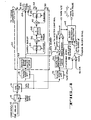
- FIGURE 1 is a block diagram of the clock generator of this invention;
- FIGURES 2a-c are waveforms representing the timing relation of early and late video signals;
- FIGURE 3 is a sinusoidal waveform representing the input analog burst signal and the digitized filtered samples A and B;
- FIGURE 4 is a schematic block diagram of the high speed digital signal processor of FIG. 1;
- FIGURE 5 is a schematic block diagram of the frequency synthesizer of FIG. 1;
- FIGURES 6a-c depict burst samples representing change with reference to clock phase error;
- FIGURES 7a and 7b represent the phase error angle ϑ between clock samples and burst zero crossings;
- FIGURES 8a-c show the outputs of the phase accumulator, digital-to-analog converter and low pass filter respectively, of the frequency synthesizer of FIG. 5; and
- FIGURE 9 portrays the relation of the 4x subcarrier sync samples relative to a defined slice level obtained from digitized sync edge detection.
- With reference to FIG. 1, a composite analog video signal is derived from a prerecorded magnetic tape and passed through a
delay circuit 10 providing a delay of one horizontal line, i.e., 63.5 µsec. plus 3.5 µsec, or a total delay of approximately 67.0 µsec. This delay produces a "late video" signal and allows a look ahead at the phase of the burst signal at the beginning and at the end of each horizontal line to determine whether any changes in phase have occurred during the period of the horizontal line under consideration. A delay of more than one television line enables the video input to switch dynamically between the delayed burst signal and the burst of the undelayed signal, so that both burst signals are applied through agated switch 12 to an analog-to-digital converter 14. The delayed analog signal is applied to thegated switch 12 which is normally in the "late video" position, but switches to "input video" or "early video" during the input video burst time. The output signal from the timed switch contains active video and burst components and the leading edge of the horizontal sync from the late video signal, as well as the burst component of the input or early video signal. The timing relationship of the early and late video signals and the combined signal obtained from the output circuit of thegated switch 12 are delineated in FIG. 2. - The combined signal is passed to the analog-to-
digital converter 14, which samples the video output signal from theswitch 12 at four times the subcarrier frequency, digitized to nine-bit words. Each digital word having sync and burst is processed by the time base correction circuit of this invention to determine and compensate phase and frequency errors that occur between the input video and a 4fsc (4x subcarrier frequency) clock. The digitized signal, containing the early burst and late burst components, is passed through a synclow pass filter 16 and aburst bandpass filter 18. Thefilter 18 averages about six cycles of each burst to reject chroma noise. For each burst, thebandpass filter 18 produces two filtered samples, designated as "A" and "B", which are 90° apart, as illustrated in FIG. 3. As shown in FIG. 3, the filtered samples A and B comprise the odd and even samples respectively, which are averaged about a baseline by adding the differences between each pair of samples in one complete cycle. - The filtered burst samples A and B are applied to a high speed
digital signal processor 20 which is illustrated in detail and will be described with reference to FIG. 4. Thesignal processor 20 calculates the sync and burst phase errors relative to the clock generated in a closed feedback loop, which includes theprocessor 20, adigital frequency synthesizer 22 that operates under control of a fixed reference clock orcrystal oscillator 24, and an analogphase lock loop 26 operating at a frequency 4 times the subcarrier frequency fsc. The feedback clock signal is returned vialead 25 to theconverter 14 and to thefilters - The burst samples A and B are used to develop a signal that represents the phase error between the signal obtained from the
phase lock loop 26, which provides a four times subcarrier sampling clock (4fsc) and the zero crossings of the off-tape burst signal. The burst samples are changed with relation to the clock phase error as depicted in FIG. 6. Sample A is negative when the clock is advanced in phase, and positive when the clock is delayed in phase. When there is no clock phase error, burst sample A is at zero, and burst sample B is displaced by 90°, as shown in FIG. 6c. Since sample A does not follow the phase error in a linear fashion, a clock to burstphase calculator 32, shown in FIG. 4, calculates the phase error angle ϑ between the 4fsc clock samples and the burst zero crossings, employing the equation recited in FIG. 7. The error signal ϑ represents the phase error between the clock and burst over 360°, and is independent of burst amplitude. It is noted that ϑ depends only on the ratio of sample A to sample B. The arctangent of the ratio of these two values define the sampling position of the burst. The arctangent of is valid only for ϑ over the range of ±90°. To obtain phase error over the entire 360° range, thecalculator 32 senses the sign of sample B and adds 180° to ϑ if sample B is negative. The clock phase error value for the late burst is directed to aswitch 64 which enables line-by-line phase correction of the clock by the frequency synthesizer. The clock-to-burst calculator 32 passes the phase error values from early burst to a burst phase subtractor including a register andsubtractor circuit 36. The subtractor circuit gives the phase error across a line. The clock phase error across a line is then applied to aconstant scaler 38, and an 40 which forms a frequency accumulator withregister 42 that is timed by the horizontal clock pulse. TheK scaler 38 converts the phase error across a line to frequency error. - If there is no frequency error between the video signal and the subcarrier clock signal, then there is no accumulated phase error across a horizontal line. Velocity compensation is achieved by setting the clock subcarrier frequency to be equal to the offtape video subcarrier frequency at the start of each line The clock determines the frequency error between the input video and the clock by measuring the phase error that accumulates across a line relative to the current subcarrier clock. The phase error is obtained by comparing two consecutive bursts of the input video to the current clock. If no frequency error exists, the clock-to-burst phase measurement of one burst is the same as for the next burst. The
burst phase subtractor - The clock frequency error signal from the
K scaler 38 represents the amount by which the frequency of the clock must be changed to match the input signal frequency. The current clock frequency value is maintained by the frequency accumulator, consisting of theadder 40 andshift register 42. For each horizontal line, the frequency error is added to the current subcarrier clock frequency to form a new clock frequency, which replaces the previous frequency value as theregister 42 is clocked for each line. The frequency accumulator allows the clock to lock its frequency to that of the input signal in a closed loop configuration. If the clock is low in frequency, the frequency error will be positive and the current clock frequency will increase until the error is zero. Similarly, if the clock is high in frequency, the error will be negative and the clock frequency will decrease until the error is zero. The output of the frequency accumulator is a 20-bit frequency control word that is passed to thefrequency synthesizer 22. - The
frequency synthesizer 22, which is the digital equivalent of a voltage controlled oscillator (VCO), operates to correct the phase of the 4x subcarrier clock on a line-by-line basis. As depicted in FIG. 5, the synthesizer includes aphase accumulator 43, consisting of anadder 44 and register 46, under control of thereference clock 24, which provides a fixed 20.46 MHz timing signal. The updated frequency control word fromregister 42 of theprocessor 20 is fed to thephase accumulator 43 of thefrequency synthesizer 22. FIG. 8a illustrates the phase accumulator operating at the subcarrier frequency of 3.58 MHz. If using another format than the NTSC standard, for example the PAL or PAL-M formats, the phase accumulator is programmed for 4.43 MHz by choosing a larger phase increment. - The phase accumulator generates a digital ramp (FIG. 8b) at the desired output frequency (fsc). The phase accumulator, which is clocked at a constant rate by the
crystal oscillator 24, provides an output signal to register 46 of a 20-bit binary number representing 360° of phase. Each time the phase accumulator is clocked by the 20.46 MHz clock, the phase advances by an amount equal to the value of the frequency control word. The phase continues to increase until it exceeds 360°. At this point, the accumulator overflows and the phase wraps around to a number less than 360°, derived from the current phase and the phase increment represented by the control word. For example, if the current phase is 350° and the phase increment or control word is 27°, the accumulator overflows to 17°. The phase will cycle through 360° of range at a rate proportional to the phase increment or frequency control word. The frequency of the phase accumulator output signal is directly related to the value of the phase increment or the frequency control word. - The digital ramp waveform generated by the phase accumulator is converted to a digital representation of a sine wave form by the
sine lookup PROM 48. The PROM converts the digital signal from the phase accumulator to a sine wave amplitude, and functions to convert 360° of phase to one full sine wave cycle. The output signal from the sine PROM is a digital word that is converted by the digital-to-analog converter 50 to a series of voltage levels which represent the instantaneous amplitude of the sine wave, as depicted in FIG. 8b. The output from the digital-to-analog converter is sinusoidal, but contains sampling steps at the 20.46 MHz clock rate, which are removed by alow pass filter 52 with a 7 MHz cutoff frequency. The result is a pure fundamental sine wave having the correct frequency of 3.58 MHz, such as shown in FIG. 8c. - Since the video signal is digitized at 4x the subcarrier, (4fsc), the sinusoidal subcarrier frequency from the tape must be multiplied by 4. This is accomplished in the
phase lock loop 26, which conventionally contains a phase comparator, a loop filter, a voltage controlled oscillator (VCO), and a divide by 4 counter. Thephase lock loop 26 settles rapidly to the line-by-line phase corrections that are applied to the tape subcarrier phase viaswitch 64 and thus has a very high bandwidth. Also, as a result, phase noise generated by the analog VCO is suppressed. - The digital sync
low pass filter 16 operates to average several adjacent video samples to form each output samplee, and is used in conjunction with burst to provide filtered chroma line type signals that are used by a memory control to maintain a correct color at the output of the timing base correction system. The digitized sync leading edge from late video which is applied to thefilter 16 is utilized by the tape clock to generate horizontal timing signals. - To obtain chroma line signals for use by the memory control of the system, the digitized late video signal that is processed by the analog-to-
digital converter 14 is applied to the digital synclow pass filter 16. The filtered signal is compared in acomparator 56 which generates coarse sliced sync signals that go high when the video sync samples cross below a predetermined slice level. As shown in FIG. 9, the detected digitized sync leading edge signals are sampled at the 4fsc rate and accurate timing information is obtained by the clock-to-sync phase calculator 54. To find a point where the sync crosses the 50% slice level to an accuracy of a few degress of subcarrier frequency, the phase between the sync slice crossing and the first clock sample below the slice level, designated as L, is computed by determining the phase ϑcs which is equal to 90° times (S-L)/(U-L), where S is the 50% slice level, U is the sample just above the slice level and L is the sample just below the slice level. - The late video sync signal that is provided by the
phase calulator 54 contains sync-to-burst phase information that is applied to anadder 56 which produces a measured sync-subcarrier phase (scH) of the offtape signal for each horizontal line. The measurement is defined over 360° and is nominally 0° for video lines with positive burst polarity and 180° for negative burst lines. By comparing the measured syncsubcarrier phase signal to a phase reference in comparator 60, a burst polarity signal H/2 (where H is at horizontal rate) is obtained for further utilization. The phase reference is set midway between the two scH values for positive and negative burst types to afford maximum immunity to noise. - In addition, a horizontal write pulse is produced by means of a
comparator 58 coupled to receive the filtered sync signal from thelow pass filter 16. Thecomparator 58 provides a coarse sliced sync signal to aburst crossing selector 62, which produces an H write pulse timed to the burst zero crossing phase. The burst zero crossing is selected by generating a one cycle wide window timed to the 50% slice point of the leading edge of the late sync signals. This window is delayed from sync so that its center is coincident with burst zero crossings of a standard scH phase signal. The positive zero crossing closest to the center of the window is selected for timing if H/2 is low, i.e., a positive burst is present, while the negative zero crossing nearest the window center is selected if H/2 is high, when a negative burst is present. - There has been decribed herein a time base correction circuit for use in a television signal video recording and playback system wherein a 4x subcarrier frequency digital clock is generated and locked in phase and frequency to the input video and burst signals derived off the recording tape. The clock follows the timing variations of the offtape signal over all speed ranges of the playback machine. The clock provides a horizontal timing pulse that is timed to a selected burst zero crossing of the offtape signal. The timing pulse is used by the timing correction circuit to define the start of each horizontal line stored in a memory. All timing error measurement is based on digitized sync and burst signals obtained from the analog-to-digital converter at the input to the correction circuitry, obviating the need for a separate analog phase comparator with associated circuitry.
Claims (20)
means (10) for delaying said input video signals to provide a delayed late video signal and an undelayed early video signal;
a converter (14) for sampling said video signals in accordance with a sampling clock at a multiple frequency of said subcarrier and for converting said delayed and undelayed analog video signals to digital signals;
a high speed digital signal processor (20) coupled to said converter for correcting the phase of the sampling clock and for providing a frequency control word;
a frequency synthesizer (22) coupled to said processor for correcting the frequency of said sampling clock in response to said frequency control word; and
means (26) operating at a multiple of the subcarrier frequency for locking the sampling clock to the video signal with correct phase and frequency on a line-by-line basis.
digitizing said sync and color burst signals;
generating a sampling clock that is locked in phase to said digitized burst signal;
measuring the difference between the phase of the color burst component and the phase of the sampling clock to provide a correction signal; and
servomechanically removing the phase error from said digitized signal in response to said correction signal.
Priority Applications (1)
| Application Number | Priority Date | Filing Date | Title |
|---|---|---|---|
| AT86307401T ATE59125T1 (en) | 1985-09-27 | 1986-09-25 | CORRECTION OF TIME BASE ERROR IN TELEVISION SIGNALS. |
Applications Claiming Priority (2)
| Application Number | Priority Date | Filing Date | Title |
|---|---|---|---|
| US06/781,293 US4675724A (en) | 1985-09-27 | 1985-09-27 | Video signal phase and frequency correction using a digital off-tape clock generator |
| US781293 | 1985-09-27 |
Publications (3)
| Publication Number | Publication Date |
|---|---|
| EP0217647A2 true EP0217647A2 (en) | 1987-04-08 |
| EP0217647A3 EP0217647A3 (en) | 1989-05-10 |
| EP0217647B1 EP0217647B1 (en) | 1990-12-12 |
Family
ID=25122280
Family Applications (1)
| Application Number | Title | Priority Date | Filing Date |
|---|---|---|---|
| EP86307401A Expired - Lifetime EP0217647B1 (en) | 1985-09-27 | 1986-09-25 | Time base correction of television signals |
Country Status (6)
| Country | Link |
|---|---|
| US (1) | US4675724A (en) |
| EP (1) | EP0217647B1 (en) |
| JP (1) | JPH0691670B2 (en) |
| AT (1) | ATE59125T1 (en) |
| CA (1) | CA1275497C (en) |
| DE (1) | DE3676149D1 (en) |
Cited By (2)
| Publication number | Priority date | Publication date | Assignee | Title |
|---|---|---|---|---|
| DE3827798A1 (en) * | 1987-08-18 | 1989-03-09 | Mitsubishi Electric Corp | Time-base error correction device |
| GB2255681A (en) * | 1991-05-08 | 1992-11-11 | Sony Corp | Analog-to-digital converter |
Families Citing this family (27)
| Publication number | Priority date | Publication date | Assignee | Title |
|---|---|---|---|---|
| US4860089A (en) * | 1987-04-10 | 1989-08-22 | Ampex Corporation | Apparatus and method for tracking the subcarrier to horizontal sync of a color television signal |
| JP2548210B2 (en) * | 1987-07-21 | 1996-10-30 | 松下電器産業株式会社 | Time axis correction device |
| US4989073A (en) * | 1987-11-25 | 1991-01-29 | Ampex Corporation | System for compensating timing errors during sampling of signals |
| US4847678A (en) * | 1988-01-11 | 1989-07-11 | Eastman Kodak Company | Dual mode gen-lock system which automatically locks to color burst or to sync information |
| JP2656288B2 (en) * | 1988-02-29 | 1997-09-24 | 株式会社東芝 | Phase detection circuit |
| US5097364A (en) * | 1988-12-12 | 1992-03-17 | Mitsubishi Denki Kabushiki Kaisha | Magnetic recording and reproducing apparatus and method of recording and reproducing |
| US5745314A (en) * | 1989-09-27 | 1998-04-28 | Canon Kabushiki Kaisha | Clock generating circuit by using the phase difference between a burst signal and the oscillation signal |
| JP2734806B2 (en) * | 1991-06-04 | 1998-04-02 | 松下電器産業株式会社 | Color burst signal phase error detection circuit |
| US5459524A (en) * | 1991-11-18 | 1995-10-17 | Cooper; J. Carl | Phase modulation demodulator apparatus and method |
| US5379077A (en) * | 1991-12-12 | 1995-01-03 | Brooktree Corporation | System for and method of, operating upon NTSC and PAL signals |
| US5495202A (en) * | 1993-06-30 | 1996-02-27 | Hughes Aircraft Company | High spectral purity digital waveform synthesizer |
| KR0134309B1 (en) * | 1994-03-11 | 1998-04-23 | 김광호 | Digital frequence automatic control circuit |
| US5566189A (en) * | 1994-08-31 | 1996-10-15 | Hughes Aircraft Co. | Method and device for puncturing data |
| US5790566A (en) * | 1994-08-31 | 1998-08-04 | Hughes Electronics | Method and device for depuncturing data |
| US5600379A (en) * | 1994-10-13 | 1997-02-04 | Yves C. Faroudia | Television digital signal processing apparatus employing time-base correction |
| US6836295B1 (en) | 1995-12-07 | 2004-12-28 | J. Carl Cooper | Audio to video timing measurement for MPEG type television systems |
| US6380980B1 (en) * | 1997-08-25 | 2002-04-30 | Intel Corporation | Method and apparatus for recovering video color subcarrier signal |
| US7605867B1 (en) | 2003-05-20 | 2009-10-20 | Pixelworks, Inc. | Method and apparatus for correction of time base errors |
| US7365796B1 (en) | 2003-05-20 | 2008-04-29 | Pixelworks, Inc. | System and method for video signal decoding using digital signal processing |
| US7701512B1 (en) | 2003-05-20 | 2010-04-20 | Pixelworks, Inc. | System and method for improved horizontal and vertical sync pulse detection and processing |
| US7304688B1 (en) | 2003-05-20 | 2007-12-04 | Pixelworks, Inc. | Adaptive Y/C separator |
| US7420625B1 (en) | 2003-05-20 | 2008-09-02 | Pixelworks, Inc. | Fuzzy logic based adaptive Y/C separation system and method |
| US7532254B1 (en) | 2003-05-20 | 2009-05-12 | Pixelworks, Inc. | Comb filter system and method |
| JP4679872B2 (en) * | 2004-10-13 | 2011-05-11 | パナソニック株式会社 | Clock generator |
| KR20060091655A (en) * | 2005-02-16 | 2006-08-21 | 삼성전자주식회사 | Method and apparatus for scanning a image signal |
| US7649569B2 (en) * | 2005-05-24 | 2010-01-19 | Texas Instruments Incorporated | Time base correction in video systems |
| US9369263B1 (en) | 2015-06-30 | 2016-06-14 | International Business Machines Corporation | Calibration of sampling phase and aperature errors in multi-phase sampling systems |
Citations (2)
| Publication number | Priority date | Publication date | Assignee | Title |
|---|---|---|---|---|
| US4249198A (en) | 1978-03-08 | 1981-02-03 | Nippon Electric Co., Ltd. | Phase locking system for television signals |
| EP0074597A2 (en) | 1981-09-15 | 1983-03-23 | Siemens Aktiengesellschaft | Method and apparatus for the digital adjustment of the clock-signal phase in a digital signal processing system |
Family Cites Families (22)
| Publication number | Priority date | Publication date | Assignee | Title |
|---|---|---|---|---|
| US3578902A (en) * | 1968-08-28 | 1971-05-18 | Rca Corp | Apparatus for synchronized generation of a signal from a composite color video signal subjected to signal perturbations |
| US4107736A (en) * | 1971-12-20 | 1978-08-15 | Image Transform, Inc. | Noise reduction system for video signals |
| US3860952B2 (en) * | 1973-07-23 | 1996-05-07 | Harris Corp | Video time base corrector |
| US4212027A (en) * | 1974-04-25 | 1980-07-08 | Ampex Corporation | Time base compensator |
| US4018990A (en) * | 1975-02-13 | 1977-04-19 | Consolidated Video Systems, Inc. | Digital video synchronizer |
| JPS5821872B2 (en) * | 1975-02-17 | 1983-05-04 | ソニー株式会社 | Pulse heart warmer |
| US4081826A (en) * | 1975-05-15 | 1978-03-28 | Sony Corporation | Video time base corrector |
| JPS51147121A (en) * | 1975-06-12 | 1976-12-17 | Sony Corp | Clock pulse generator |
| US4109276A (en) * | 1976-03-19 | 1978-08-22 | Rca Corporation | Memory read/write organization for a television signal processor |
| US4120000A (en) * | 1976-07-08 | 1978-10-10 | Sony Corporation | Video time base corrector |
| US4119999A (en) * | 1977-01-28 | 1978-10-10 | Ampex Corporation | Apparatus for inserting a digital sync word, phase-synchronized to the color subcarrier, in place of the horizontal sync signal |
| JPS53148317A (en) * | 1977-05-31 | 1978-12-23 | Sony Corp | Error correction unit for time axis |
| US4373168A (en) * | 1979-03-30 | 1983-02-08 | Nippon Electric Co., Ltd. | Digital time-base corrector having a wide correction range |
| US4291332A (en) * | 1980-04-10 | 1981-09-22 | Tokyo Shibaura Denki Kabushiki Kaisha | Phase-locked circuit |
| US4404531A (en) * | 1980-06-05 | 1983-09-13 | Motorola, Inc. | Frequency scanning apparatus wherein a single knob controls both step size and direction of change |
| JPS57106285A (en) * | 1980-12-22 | 1982-07-02 | Sony Corp | Time base collector |
| JPS5835703A (en) * | 1981-08-24 | 1983-03-02 | Asahi Optical Co Ltd | Reproducer for recording information |
| US4563657A (en) * | 1982-03-15 | 1986-01-07 | Codex Corporation | Frequency synthesizer and digital phase lock loop |
| US4463371A (en) * | 1982-05-28 | 1984-07-31 | Rca Corporation | Clock generation apparatus for a digital television system |
| JPS6080387A (en) * | 1983-10-11 | 1985-05-08 | Sony Corp | Digitizing circuit of color video signal |
| US4612568A (en) * | 1984-11-05 | 1986-09-16 | Rca Corporation | Burst-to-line-locked clock digital video signal sample rate conversion apparatus |
| US4633298A (en) * | 1984-11-30 | 1986-12-30 | Rca Corporation | Digitally controlled phase locked loop system having coarse and fine locking modes |
-
1985
- 1985-09-27 US US06/781,293 patent/US4675724A/en not_active Expired - Lifetime
-
1986
- 1986-08-26 JP JP61199868A patent/JPH0691670B2/en not_active Expired - Lifetime
- 1986-09-24 CA CA000518950A patent/CA1275497C/en not_active Expired - Lifetime
- 1986-09-25 AT AT86307401T patent/ATE59125T1/en not_active IP Right Cessation
- 1986-09-25 EP EP86307401A patent/EP0217647B1/en not_active Expired - Lifetime
- 1986-09-25 DE DE8686307401T patent/DE3676149D1/en not_active Expired - Lifetime
Patent Citations (2)
| Publication number | Priority date | Publication date | Assignee | Title |
|---|---|---|---|---|
| US4249198A (en) | 1978-03-08 | 1981-02-03 | Nippon Electric Co., Ltd. | Phase locking system for television signals |
| EP0074597A2 (en) | 1981-09-15 | 1983-03-23 | Siemens Aktiengesellschaft | Method and apparatus for the digital adjustment of the clock-signal phase in a digital signal processing system |
Cited By (5)
| Publication number | Priority date | Publication date | Assignee | Title |
|---|---|---|---|---|
| DE3827798A1 (en) * | 1987-08-18 | 1989-03-09 | Mitsubishi Electric Corp | Time-base error correction device |
| US5072315A (en) * | 1987-08-18 | 1991-12-10 | Mitsubishi Denki Kabushiki Kaisha | Time axis correcting device |
| GB2255681A (en) * | 1991-05-08 | 1992-11-11 | Sony Corp | Analog-to-digital converter |
| US5325093A (en) * | 1991-05-08 | 1994-06-28 | Sony Corporation | Analog-to-digital converter for composite video signals |
| GB2255681B (en) * | 1991-05-08 | 1994-09-07 | Sony Corp | Analog-to-digital converter |
Also Published As
| Publication number | Publication date |
|---|---|
| EP0217647B1 (en) | 1990-12-12 |
| ATE59125T1 (en) | 1990-12-15 |
| CA1275497C (en) | 1990-10-23 |
| EP0217647A3 (en) | 1989-05-10 |
| DE3676149D1 (en) | 1991-01-24 |
| JPH0691670B2 (en) | 1994-11-14 |
| JPS6277792A (en) | 1987-04-09 |
| US4675724A (en) | 1987-06-23 |
Similar Documents
| Publication | Publication Date | Title |
|---|---|---|
| EP0217647A2 (en) | Time base correction of television signals | |
| EP0189195B1 (en) | Apparatus for correcting time base error of video signal | |
| EP0152922B1 (en) | Method and system for processing digital video signal incorporating phase-correction feature | |
| WO2000054519A1 (en) | Time base corrector | |
| CA1277724C (en) | Digital phase-locked loops | |
| US4772950A (en) | Method and apparatus for sampling and processing a video signal | |
| US5677743A (en) | Apparatus and method for synchronizing a horizontal deflection signal with a horizontal sync signal | |
| US4797730A (en) | Method and apparatus for controlling the sampling phase of an analog color television signal | |
| US5929923A (en) | Apparatus for producing a video signal in synchronism with an external synchronizing signal | |
| US5121207A (en) | Digital circuit arrangement for processing an analog video signal at a free running system clock | |
| US6380980B1 (en) | Method and apparatus for recovering video color subcarrier signal | |
| KR100221438B1 (en) | Synchronous clock generation circuit | |
| US5206726A (en) | Time base corrector for eliminating time base fluctuations in a composite video signal | |
| US4864387A (en) | PAL video time base corrector inverts color difference signal (V) axis | |
| US5272532A (en) | Horizontal AFC (automatic frequency control) circuit | |
| US5703656A (en) | Digital phase error detector for locking to color subcarrier of video signals | |
| US7425993B2 (en) | Video signal processing | |
| JPH0620249B2 (en) | Horizontal sync detection circuit | |
| US5631708A (en) | Automatic phase control apparatus | |
| JP3026695B2 (en) | Clock pulse generator | |
| JPH05207413A (en) | Processor for video signal | |
| JPS647556B2 (en) | ||
| GB2181015A (en) | Video signal processor | |
| JPH0746873B2 (en) | Sampling clock generation circuit for A / D conversion | |
| JPH0984039A (en) | Sampling clock generator |
Legal Events
| Date | Code | Title | Description |
|---|---|---|---|
| PUAI | Public reference made under article 153(3) epc to a published international application that has entered the european phase |
Free format text: ORIGINAL CODE: 0009012 |
|
| AK | Designated contracting states |
Kind code of ref document: A2 Designated state(s): AT CH DE FR GB IT LI NL |
|
| PUAL | Search report despatched |
Free format text: ORIGINAL CODE: 0009013 |
|
| AK | Designated contracting states |
Kind code of ref document: A3 Designated state(s): AT CH DE FR GB IT LI NL |
|
| 17P | Request for examination filed |
Effective date: 19890527 |
|
| 17Q | First examination report despatched |
Effective date: 19890811 |
|
| GRAA | (expected) grant |
Free format text: ORIGINAL CODE: 0009210 |
|
| AK | Designated contracting states |
Kind code of ref document: B1 Designated state(s): AT CH DE FR GB IT LI NL |
|
| REF | Corresponds to: |
Ref document number: 59125 Country of ref document: AT Date of ref document: 19901215 Kind code of ref document: T |
|
| ET | Fr: translation filed | ||
| REF | Corresponds to: |
Ref document number: 3676149 Country of ref document: DE Date of ref document: 19910124 |
|
| ITF | It: translation for a ep patent filed |
Owner name: BARZANO' E ZANARDO ROMA S.P.A. |
|
| ITTA | It: last paid annual fee | ||
| PLBE | No opposition filed within time limit |
Free format text: ORIGINAL CODE: 0009261 |
|
| STAA | Information on the status of an ep patent application or granted ep patent |
Free format text: STATUS: NO OPPOSITION FILED WITHIN TIME LIMIT |
|
| 26N | No opposition filed | ||
| PGFP | Annual fee paid to national office [announced via postgrant information from national office to epo] |
Ref country code: AT Payment date: 19930909 Year of fee payment: 8 |
|
| PGFP | Annual fee paid to national office [announced via postgrant information from national office to epo] |
Ref country code: CH Payment date: 19930929 Year of fee payment: 8 |
|
| PGFP | Annual fee paid to national office [announced via postgrant information from national office to epo] |
Ref country code: NL Payment date: 19930930 Year of fee payment: 8 |
|
| REG | Reference to a national code |
Ref country code: GB Ref legal event code: 732E |
|
| NLS | Nl: assignments of ep-patents |
Owner name: AMPEX SYSTEMS CORPORATION TE REDWOOD CITY, CALIFOR |
|
| PG25 | Lapsed in a contracting state [announced via postgrant information from national office to epo] |
Ref country code: AT Effective date: 19940925 |
|
| PG25 | Lapsed in a contracting state [announced via postgrant information from national office to epo] |
Ref country code: CH Effective date: 19940930 Ref country code: LI Effective date: 19940930 |
|
| PG25 | Lapsed in a contracting state [announced via postgrant information from national office to epo] |
Ref country code: NL Effective date: 19950401 |
|
| NLV4 | Nl: lapsed or anulled due to non-payment of the annual fee | ||
| REG | Reference to a national code |
Ref country code: CH Ref legal event code: PL |
|
| REG | Reference to a national code |
Ref country code: GB Ref legal event code: 732E |
|
| REG | Reference to a national code |
Ref country code: GB Ref legal event code: IF02 |
|
| PGFP | Annual fee paid to national office [announced via postgrant information from national office to epo] |
Ref country code: DE Payment date: 20040923 Year of fee payment: 19 |
|
| PGFP | Annual fee paid to national office [announced via postgrant information from national office to epo] |
Ref country code: FR Payment date: 20050823 Year of fee payment: 20 |
|
| PGFP | Annual fee paid to national office [announced via postgrant information from national office to epo] |
Ref country code: GB Payment date: 20050921 Year of fee payment: 20 |
|
| PG25 | Lapsed in a contracting state [announced via postgrant information from national office to epo] |
Ref country code: IT Free format text: LAPSE BECAUSE OF NON-PAYMENT OF DUE FEES;WARNING: LAPSES OF ITALIAN PATENTS WITH EFFECTIVE DATE BEFORE 2007 MAY HAVE OCCURRED AT ANY TIME BEFORE 2007. THE CORRECT EFFECTIVE DATE MAY BE DIFFERENT FROM THE ONE RECORDED. Effective date: 20050925 |
|
| REG | Reference to a national code |
Ref country code: GB Ref legal event code: PE20 |
|
| PG25 | Lapsed in a contracting state [announced via postgrant information from national office to epo] |
Ref country code: DE Free format text: LAPSE BECAUSE OF NON-PAYMENT OF DUE FEES Effective date: 20060401 |
|
| PG25 | Lapsed in a contracting state [announced via postgrant information from national office to epo] |
Ref country code: GB Free format text: LAPSE BECAUSE OF EXPIRATION OF PROTECTION Effective date: 20060924 |