EP0212764A2 - High density, controlled impedance connector - Google Patents
High density, controlled impedance connector Download PDFInfo
- Publication number
- EP0212764A2 EP0212764A2 EP86300288A EP86300288A EP0212764A2 EP 0212764 A2 EP0212764 A2 EP 0212764A2 EP 86300288 A EP86300288 A EP 86300288A EP 86300288 A EP86300288 A EP 86300288A EP 0212764 A2 EP0212764 A2 EP 0212764A2
- Authority
- EP
- European Patent Office
- Prior art keywords
- high density
- wafers
- electrical connector
- conductive
- conductive elements
- Prior art date
- Legal status (The legal status is an assumption and is not a legal conclusion. Google has not performed a legal analysis and makes no representation as to the accuracy of the status listed.)
- Ceased
Links
Images


Classifications
-
- H—ELECTRICITY
- H01—ELECTRIC ELEMENTS
- H01R—ELECTRICALLY-CONDUCTIVE CONNECTIONS; STRUCTURAL ASSOCIATIONS OF A PLURALITY OF MUTUALLY-INSULATED ELECTRICAL CONNECTING ELEMENTS; COUPLING DEVICES; CURRENT COLLECTORS
- H01R12/00—Structural associations of a plurality of mutually-insulated electrical connecting elements, specially adapted for printed circuits, e.g. printed circuit boards [PCB], flat or ribbon cables, or like generally planar structures, e.g. terminal strips, terminal blocks; Coupling devices specially adapted for printed circuits, flat or ribbon cables, or like generally planar structures; Terminals specially adapted for contact with, or insertion into, printed circuits, flat or ribbon cables, or like generally planar structures
- H01R12/70—Coupling devices
- H01R12/71—Coupling devices for rigid printing circuits or like structures
- H01R12/72—Coupling devices for rigid printing circuits or like structures coupling with the edge of the rigid printed circuits or like structures
- H01R12/721—Coupling devices for rigid printing circuits or like structures coupling with the edge of the rigid printed circuits or like structures cooperating directly with the edge of the rigid printed circuits
-
- H—ELECTRICITY
- H01—ELECTRIC ELEMENTS
- H01R—ELECTRICALLY-CONDUCTIVE CONNECTIONS; STRUCTURAL ASSOCIATIONS OF A PLURALITY OF MUTUALLY-INSULATED ELECTRICAL CONNECTING ELEMENTS; COUPLING DEVICES; CURRENT COLLECTORS
- H01R13/00—Details of coupling devices of the kinds covered by groups H01R12/70 or H01R24/00 - H01R33/00
- H01R13/648—Protective earth or shield arrangements on coupling devices, e.g. anti-static shielding
- H01R13/658—High frequency shielding arrangements, e.g. against EMI [Electro-Magnetic Interference] or EMP [Electro-Magnetic Pulse]
- H01R13/6581—Shield structure
- H01R13/6585—Shielding material individually surrounding or interposed between mutually spaced contacts
- H01R13/6586—Shielding material individually surrounding or interposed between mutually spaced contacts for separating multiple connector modules
- H01R13/6587—Shielding material individually surrounding or interposed between mutually spaced contacts for separating multiple connector modules for mounting on PCBs
Definitions
- the present invention relates to a high density, controlled impedance connector and, more particularly, to a high density connector which may be utilized to mate a plurality of modules (daughter boards) to a backplane (mother board) wherein each electrical connection has a controlled impedance and a minimum amount of crosstalk.
- a flat cable formed with a plurality of flat conductors and surrounded on its upper and lower surface by a ground plane, thus forming a stripline may be found in U.S. Letters Patent No. 3,612,744, issued October 12, 1971 and invented by P.J. Thomas.
- a second flat cable in the form of a microstrip is described in U.S. Letters Patent No. 4,441,088, which issued April 3, 1984 by C.J. Anderson.
- the Anderson patent discusses the reduction of crosstalk by adjusting the amount of dielectric material between the flat conductor and the ground plane in proportion to the amount of dielectric material placed over the flat conductor.
- a later connector for shielding electrical contacts therein to permit a high frequency signal to pass there through utilizing a stripline configuration is shown in an IBM Technical Disclosure Bulletin, Volume 10, No. 3, August 1967, pp. 203-4. This connector does not contemplate a high density connector as in the present invention.
- a further object is to provide a high density connector which may be easily configured to accomodate different sized printed circuit boards and different mounting configurations.
- Yet a further object is to provide a configuration for an electrical connector which may be easily replaced and repaired.
- a still further object of this invention is to provide a high density, controlled impedance connector, which is economic, flexible and expandable.
- a discrete wafer formed from a dielectric material having a plurality of conductive elements mounted by said wafer.
- a single, ground plane element for connection to an electrical ground is also mounted by the wafer.
- the discrete wafers are then stacked side-by-side in an arrangement which permits the ground plane, mounted by two wafers, to surround the plurality of conductive elements, mounted by a single discrete wafer. This arrangement creates a stripline configuration for the plurality of conductive elements, whose configuration controls the impedance of the conductive elements.
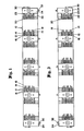
- Figs. 1-5 illustrate one embodiment of the high density connector 10 wherein Fig. 1 is a side view showing various components of the connector including a discrete wafer 12 which, in'this alternative embodiment, mounts a plurality of signal carrying contact elements 14 adjacent to which is mounted a single ground plane element 16.
- a discrete wafer 12 which, in'this alternative embodiment, mounts a plurality of signal carrying contact elements 14 adjacent to which is mounted a single ground plane element 16.
- Each discrete wafer 12 is placed in a side-by-side stack with other discrete wafers 12 having ground plane elements 16 placed therebetween as best seen in Fig. 4.
- the individual contact elements 14 are encapsulated within the insulating, dielectric material of wafer 14 and surrounded on each side by ground planes 16 for creating a stripline arrangement for each contact element 14.
- the individual contact elements 14 are fabricated to form a ninety degree turn (Fig. 5) which is terminated at each end by a pair of spring wiping finger 18.
- the ground plane elements 16 are each provided with four spring wiping fingers 19 (Fig. 4).
- the spring fingers 18 and 19 are bent at an angle to the right in Figs. 1, 2 and 4 with fingers 18 extending from each wafer 12 at a surface which has been recessed at 20 to permit flexure in the right-hand direction.
- the right-hand flexure of the spring fingers 18 and 19 fits over adjacent spring fingers so that a high density of these fingers may be accommodated within the side-by-side stack of wafers 12.
- a spacer 22 is provided at the far right edge of each stack, followed by a mounting bracket 24.
- the ground plane element 16 and spacers 22 have a configuration similar to the configuration of wafer 12 including a recess 23. It may now be seen that the purpose of the spacer 22 and its recess 23 is to provide an area into which the spring fingers 18 and 19 may flex when the connector 10 is assembled against a printed circuit board.
- the addition of the mounting brackets 24 on opposite sides of the wafer stack completes the assembly.
- the wafers 12, ground plane elements 16, spacers 22 and mounting brackets 24 are assembled in a stack which may be formed by a series of repeated parts to any desired length. These parts are provided with a plurality of apertures including three smaller apertures 25 for receiving a set of locating shafts 26 and a larger aperture 27 for receiving a support shaft 28.
- the connector 10 is thus assembled by stacking a mounting bracket 24 on the left-hand end of the stack followed by a ground plane element 16, a wafer 12, and a ground plane element 16 until a predetermined number of wafers and ground plane elements have been stacked upon the shafts 26 and 28. It should be noted here that the number of ground plane elements 16 is one more than the ground plane elements 12.
- the stack is then followed by a spacer 22 which provides the recesses 23 into which the spring fingers 18 for contacts 14 and spring fingers 19 for ground plane 16 extend.
- the next element in the stack is a second mounting bracket 24.
- the stack is typically 12" x 1/2" x 1/2" in size.
- the support shaft 28 receives a screw 30 at each end whose threads pass through a clearance hole in bracket 24 into the internally threaded end of shaft 28 for compressing and retaining the 12" stack in its desired configuration.
- each bracket 24 having four locating pins 32 extending from two adjacent surfaces.
- a first surface mounts a backplane or mother board 34 wherein locating pins 32 are received by apertures 36 within the board 34.
- Mounted at a right angle, or ninety degrees to the mother board 34 is a module or daughter board 38, also having apertures 36 therein for receiving the locating pins 32.
- the mother and daughter boards 34 and 38 are retained against the connector 10 by suitable fastening means, such as screws 40.
- suitable fastening means such as screws 40.
- the screws 40 pass through the boards 34 and 38 into threaded holes in the mounting brackets 34.
- the wafers 12 are illustrated with the contact elements 14 encapsulated therein. It will be understood that the spring fingers 18 of contact elements 14 are compressed against the mother and daughter boards 34 and 38 within the recesses 20 to make an electrical connection therebetween.
- the spring fingers 18 contact suitable pads 42 such as those shown in Fig. 6 mounted upon the daughter board 38. Each individual pad 42 is provided with apertures 44 to make an electrical connection to the far side of the daughter board where connection with electrical conductors (not shown) is completed.
- the spring fingers 19 on the ground plane elements 16 contact a pair of conductive strips 46 on either side of the pads 42.
- the connector 10 consists of a stack of five brackets 24, four spacers 22, two hundred and four wafers 12 and two hundred and eight ground planes 14.
- the reader will remember that, in the embodiment shown, there are four substacks of wafers 12 so that the one additional ground plane 16 in each substack totals the four additional ground planes in the completed stack.
- the arrangement shown provides for eight hundred and sixteen signal contacts made by spring fingers 18 and four hundred and sixteen ground contacts made by fingers 19.
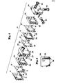
- a discrete dielectric wafer 52 is molded from suitable insulation materials, such as polysulfone, to mount a plurality of individual conductive contact elements 54, Fig. 9, on one side, and to mount a single ground plane element 56 on the other side thereof, Fig. 10.
- Each individual signal contact 54 is constructed with an arcuate curve of ninety degrees which is terminated at each end by a spring wiping fingers 58.
- the spring fingers 58 are shown in their compressed position in Figs. 9 and 10 as if pressed against a printed circuit board such as boards 34 or 38.
- the ground plane element 56 is also provided with a plurality of spring fingers 59, which coincide in their spacing with each individual spring finger 58 from the contact elements 54.
- the contact elements 54 and ground plane elements 56 may be constructed from beryllum copper or other suitable alloys.
- the dielectric wafer wafer 52 is molded into a hexagonal shape having first and second generally flat surfaces 60 and 62 (Fig. 7).
- the first surface 60 is provided with a plurality of grooves 64, eight are shown in the preferred embodiment of Fig. 8, which received the arcuate contact elements 54.
- Two edges of surface 60 arranged at right angles to one another are relieved along those edges to a depth equal to the depth of grooves 64 to form recesses 66. These recesses 66 provide clearance for the motion of the spring fingers 58 as they are pressed against the printed circuit boards.
- the second surface 62 of wafer 52 is provided with a single recess 68 which receives the ground plane element 56. Recess 68 extends to the two edges of the hexagonal wafer 52 that are arranged at ninety degrees to one another to permit the spring fingers 59 of the ground plane element 56 to be exposed to the printed circuit boards opposite fingers 58.
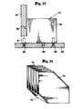
- a slotted housing 72 is provided to receive that discrete wafers 52.
- Housing 72, Fig. 14 has a hexagonal cross section and is molded from a suitable insulated material, such as polysulfone, with a plurality of slots 74 which are open along two edge surfaces arranged at a right angle to one another.
- the slots 74 are arranged to receive the wafers 52, contact elements 54, and ground planes 56.
- the housing 72 thus forms a first housing for mounting the plurality of wafers 52. Housing 72 is then inserted into an elongated opening 76 in the second housing 78. The insertion of first housing 72 into elongated openings 76 may be accomplished by removing the top of housing 78. However, in the preferred embodiment, a pie shaped piece 79 is removed. Housing 72 is then rotated slightly and inserted into opening 76 so as not to injure the spring fingers 58 and 59. By rotating the housing 72, it is possible to insert the housing 72 into slot 76 far enough to permit the clearance of contacts 58 and 59 into the left-hand opening of slot 76.
- the wedge member 79 may be replaced and retained by suitable fastening means, such as screws, not shown.
- the second housing 78 is provided with locating pins 80 and threaded apertures 81 for aligning and mounting the connector 50 to suitable printed circuit boards 82 and 84, or by screws 85, Fig. 12.
- the stack of wafers 52 comprises a ground plane 56 at the far left-hand end of the slot 76 adjacent housing 72.
- the ground plane is mounted by the wafer 52 whose next surface mounts the contact elements 54.
- This alternate stack continues until the far right-hand end of slot 76 wherein the last wafer 52 includes only the ground plane 56.
- slot 76 may mount one hundred and one wafers 52 therein having one hundred sets of contact elements 54 and one hundred and one sets of ground plane elements 56.
- This configuration mounts a total of sixteen hundred and eight spring finger contacts 54 and 56.
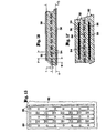
- the spring fingers 54 and 56 are shown schematically in Figs. 11 and 13 as simple dots.
- the spring fingers 58 of contact elements 54 slide across pads 86 (Fig. 15) to make electrical contact with the board 82.
- the spring fingers 59 of the ground plane elements 56 slide across conductive strips 88 to complete the stripline circuit formed by surrounding contact elements 54 by ground planes 56.
- each contact 54 has been formed with the side-by-side ground planes 56 equal distance from the contacts 54.
- the ground planes 56 are separated by a distance "b” whereas the contact elements 54 having a width "w” and a thicknes “t” are spaced from the bottom ground plane 56 by a distance "H”.
- the contacts 54 are spaced apart by a pitch "P”.
- the impedance Z o of each contact 54 may be expressed by the equation: . wherein:
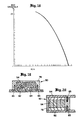
- Crosstalk within connector 50 may be reduced by providing a thicker spring finger 59 for each ground plane 56 than the related spring finger 58 for each contact 54. This configuration is shown in Fig. 17. Crosstalk may also be reduced by adjusting the ratio of the distance between two adjacent contact elements 54 or pitch "P" in proportion to the height "H" of the contacts 54 above the ground plane 56. The percentage of reduction of crosstalk versus the pitch to height ratio (P/H) is shown in Fig. 18. By adjusting the pitch of the contact elements 54 or the equal spacing of these contacts from the ground planes 56, it is possible to reduce crosstalk significantly as shown by the curve of Fig. 18.
- the connector 50 and its housing 78 may be modified wherein the contacts 54 extend through a 180 degree arc to mount the two boards 82 and 84 in a parallel in-line configuration, Fig. 19. Further, the connector 50 and its housing 78 may be modified to accommodate the contacts in a straight line configuration wherein the two boards 82 and 84 are mounted in a parallel configuration, one upon the other, Fig. 20.
- the preferred embodiment has also shown the spring fingers 58 from the contact elements 54 mounted in alternating rows with fingers 59 from the ground planes element 56. Such an arrangement is shown schematically in Fig. 21. There are other embodiments, however, where it may be desirable to place the spring fingers 58 in an immediate side-by-side relationship separated by a pair of ground plane elements 56. Such an arrangement is shown in Fig. 22. This arrangement may be easily accomplished by the present invention.
Abstract
Description
- The present invention relates to a high density, controlled impedance connector and, more particularly, to a high density connector which may be utilized to mate a plurality of modules (daughter boards) to a backplane (mother board) wherein each electrical connection has a controlled impedance and a minimum amount of crosstalk.
- In the prior art, there has been a considerable amount of discussion of the utilization of a flat cable system which might include a flat or round wire for handling high speed signals such as high speed digital pulses. The advantage of the flat cable is that one or two sides of the cable may be provided with a conductive layer which, in turn, is connected to ground. If a single conductive layer is used on one side, a microstrip is formed. When conductive layers are used on both sides, a stripline is formed. For an article discussing the mathematics and properties of such flat cables, see: Bossi, Dennis F., Testing Electrical And Transmission Properties In Flat Cable, presented at the 19th International Wire & Cable Symposium, Atlantic City, New Jersey, December, 1970.
- A flat cable formed with a plurality of flat conductors and surrounded on its upper and lower surface by a ground plane, thus forming a stripline, may be found in U.S. Letters Patent No. 3,612,744, issued October 12, 1971 and invented by P.J. Thomas. A second flat cable in the form of a microstrip is described in U.S. Letters Patent No. 4,441,088, which issued April 3, 1984 by C.J. Anderson. The Anderson patent discusses the reduction of crosstalk by adjusting the amount of dielectric material between the flat conductor and the ground plane in proportion to the amount of dielectric material placed over the flat conductor.
- The advantage of utilizing a flat cable becomes apparent after consideration of the discussions within the references cited above. That is, the dimensions of the cable may be altered to select or control the impedance and to reduce the amount of crosstalk. This concept was incorporated into an early connector wherein a dielectric sheet of resilient material was surrounded on one side by a ground plane and on the other by conductive strips. The distance between the conductive strips and the resilient ground plane was said to achieve impedance matching characteristics. See U.S. Letters Patent No. 3,401,369, issued September 10, 1968 by P.H. Palmateer, et al.
- A later connector for shielding electrical contacts therein to permit a high frequency signal to pass there through utilizing a stripline configuration is shown in an IBM Technical Disclosure Bulletin,
Volume 10, No. 3, August 1967, pp. 203-4. This connector does not contemplate a high density connector as in the present invention. - It is also known in the prior art to use a connector having a plurality of contacts mounted directly into a mother board. These contacts mate with conductive elements upon the mother board and include spring fingers that wipe conductive elements on a daughter board to make electrical connection between the daughter board and the mother board. In one such connector, shown in U.S. Letters Patent No. 3,651,432, issued March 21, 1972, by H. E. Henschen, et al., impedance matching of a microstrip circuit is accomplished by connecting a middle contact to a signal carrying element on the mother board while connecting contacts on either side thereof to a ground plane on the opposite side of the mother board. In this configuration, the signal carrying contact is surrounded by a ground connection to control and match impedance. However, this configuration is extremely bulky and does not lend itself to a high density connector system.
- Two additional connector systems utilizing round wires which are bent at ninety degrees to form contacts that are inserted into a mother board are shown in U.S. Letters Patent No. 4,070,084, issued January 24, 1978, by R.V. Hutchison, and No. 4,232,929, issued November 11, 1980, by F. Zobawa. The first patent discusses a means for controlling impedance using a microstrip arrangement by imbedding a conductive element within a dielectric substrate. An alternative arrangement shows a flexible dielectric material with a ground plane on one side and conductive elements on the other. The second patent discusses reduction of crosstalk by an intermediate ground plane located between the contacts. Each of these arrangements suffer from bulk and inability to produce a high density connector.
- Accordingly, it is an object of the present invention to provide a high density connector which is capable of producing a constant impedance and a reduced crosstalk.
- It is another object of the present invention to provide a high density connector which permits the control of impedance regardless of the length of the contact through the utilization of a stripline configuration within the connector.
- A further object is to provide a high density connector which may be easily configured to accomodate different sized printed circuit boards and different mounting configurations.
- Yet a further object is to provide a configuration for an electrical connector which may be easily replaced and repaired.
- A still further object of this invention is to provide a high density, controlled impedance connector, which is economic, flexible and expandable.
- In accomplishing these and other objects, there is provided a discrete wafer formed from a dielectric material having a plurality of conductive elements mounted by said wafer. A single, ground plane element for connection to an electrical ground is also mounted by the wafer. The discrete wafers are then stacked side-by-side in an arrangement which permits the ground plane, mounted by two wafers, to surround the plurality of conductive elements, mounted by a single discrete wafer. This arrangement creates a stripline configuration for the plurality of conductive elements, whose configuration controls the impedance of the conductive elements.
- There are several embodiments which incorporate the unique ideas of the present invention. These embodiments will be better understood after consideration of the following specification and drawings wherein:
-
- Fig. 1 is a side view showing an alternative embodiment of a high density connector incorporating the present invention;
- Fig. 2 is an end view of Fig. 1;
- Fig. 3 is a bottom plane view of Fig. 1;
- Fig. 4 is an exploded, perspective view, showing the connector illustrated in Figs. 1-3;
- Fig. 5 is a cross sectional view showing the high density connector mounting four daughter boards upon a mother board;
- Fig. 6 shows a typical layout for the conductive pads which may be utilized upon a mother board or a daughter board, mounting the connectors shown in Figs. 1-5;
- Fig. 7 is a perspective view showing an insulated discrete wafer utilized within a preferred embodiment of the present invention;
- Fig. 8 is a cross-sectional view taken along line 8-8 of Fig. 7;
- Fig. 9 is a cross-sectional view of a high density connector incorporating the wafer shown in Figs. 7 and 8;
- Fig. 10 is a cross-sectional view of the second side of the wafer shown in Fig. 9;
- Fig. 11 is a side view, similar to Fig.. 1, illustrating the preferred embodiment of a high density connector incorporating the features of the present invention;
- Fig. 12 is an end view of Fig. 11;
- Fig. 13 is a bottom plan view of the connector shown in Fig. 11;
- Fig. 14 is a perspective view showing an insulating housing which receives the discrete wafers of Fig. 7;
- Fig. 15 is a partial view showing the conductive pads, which may be utilized upon a printed circuit board mounting the connector shown in Figs. 7-14;
- Fig. 16 is a cross-sectional view taken along line 16-16 of Fig. 9;
- Fig. 17 is a cross-sectional view taken along line 17-17 of Fig. 9;
- Fig. 18 is a curve showing the maximum crosstalk as a percentage versus the pitch to height ratio (P/H) of the connector;
- Fig. 19 is a schematic representation, similar to Fig. 12, showing a connector arrangement wherein the printed circuit boards may be mounted in a parallel and aligned configuration;
- Fig. 20 is a schematic, similar to Fig. 19, presenting a connector mounting arrangement wherein the printed circuit boards may be mounted in parallel;
- Fig. 21 shows a schematic arrangement of the plurality of conductive elements shown in the connector of Figs. 7-14; and
- Fig. 22 is a schematic representation similar to Fig. 21 showing another embodiment.
- Referring now to the drawings, Figs. 1-5 illustrate one embodiment of the
high density connector 10 wherein Fig. 1 is a side view showing various components of the connector including adiscrete wafer 12 which, in'this alternative embodiment, mounts a plurality of signal carryingcontact elements 14 adjacent to which is mounted a singleground plane element 16. Eachdiscrete wafer 12 is placed in a side-by-side stack with otherdiscrete wafers 12 havingground plane elements 16 placed therebetween as best seen in Fig. 4. In this configuration, theindividual contact elements 14 are encapsulated within the insulating, dielectric material ofwafer 14 and surrounded on each side byground planes 16 for creating a stripline arrangement for eachcontact element 14. - In the embodiments shown in Figs. 1-5, it will be seen that the
individual contact elements 14 are fabricated to form a ninety degree turn (Fig. 5) which is terminated at each end by a pair ofspring wiping finger 18. Similarly, theground plane elements 16 are each provided with four spring wiping fingers 19 (Fig. 4). Thespring fingers fingers 18 extending from eachwafer 12 at a surface which has been recessed at 20 to permit flexure in the right-hand direction. As seen in Figs. 1 and 3, the right-hand flexure of thespring fingers wafers 12. Aspacer 22 is provided at the far right edge of each stack, followed by a mountingbracket 24. Theground plane element 16 andspacers 22 have a configuration similar to the configuration ofwafer 12 including arecess 23. It may now be seen that the purpose of thespacer 22 and itsrecess 23 is to provide an area into which thespring fingers connector 10 is assembled against a printed circuit board. The addition of the mountingbrackets 24 on opposite sides of the wafer stack completes the assembly. - As best seen in Fig. 4, the
wafers 12,ground plane elements 16,spacers 22 and mountingbrackets 24 are assembled in a stack which may be formed by a series of repeated parts to any desired length. These parts are provided with a plurality of apertures including threesmaller apertures 25 for receiving a set of locatingshafts 26 and alarger aperture 27 for receiving asupport shaft 28. Theconnector 10 is thus assembled by stacking a mountingbracket 24 on the left-hand end of the stack followed by aground plane element 16, awafer 12, and aground plane element 16 until a predetermined number of wafers and ground plane elements have been stacked upon theshafts ground plane elements 16 is one more than theground plane elements 12. The stack is then followed by aspacer 22 which provides therecesses 23 into which thespring fingers 18 forcontacts 14 andspring fingers 19 forground plane 16 extend. The next element in the stack is asecond mounting bracket 24. In the embodiment shown in Figs. 1-3, the stack is typically 12" x 1/2" x 1/2" in size. Thesupport shaft 28 receives ascrew 30 at each end whose threads pass through a clearance hole inbracket 24 into the internally threaded end ofshaft 28 for compressing and retaining the 12" stack in its desired configuration. In thehigh density connector 10 shown in Figs. 1-5, there are fourcontact elements 14 with correspondingspring fingers 18 mounted between the twospring fingers 19 associated with theground plane element 16. This assures good electrical isolation for the fourcontacts 14. - Referring now to Fig. 5, the
connector 10 is shown with eachbracket 24 having four locatingpins 32 extending from two adjacent surfaces. A first surface mounts a backplane ormother board 34 wherein locatingpins 32 are received byapertures 36 within theboard 34. Mounted at a right angle, or ninety degrees to themother board 34 is a module ordaughter board 38, also havingapertures 36 therein for receiving the locating pins 32. The mother anddaughter boards connector 10 by suitable fastening means, such as screws 40. As seen in the right-hand portion of Fig. 5, thescrews 40 pass through theboards brackets 34. Further down the stack ofconnector 10, as seen in the left-hand portion of Fig. 5, thewafers 12 are illustrated with thecontact elements 14 encapsulated therein. It will be understood that thespring fingers 18 ofcontact elements 14 are compressed against the mother anddaughter boards recesses 20 to make an electrical connection therebetween. - To accomplish the electrical connection, the
spring fingers 18 contactsuitable pads 42 such as those shown in Fig. 6 mounted upon thedaughter board 38. Eachindividual pad 42 is provided withapertures 44 to make an electrical connection to the far side of the daughter board where connection with electrical conductors (not shown) is completed. Thespring fingers 19 on theground plane elements 16 contact a pair ofconductive strips 46 on either side of thepads 42. - In the alternative embodiment shown in Figs. 1-5, the
connector 10 consists of a stack of fivebrackets 24, fourspacers 22, two hundred and fourwafers 12 and two hundred and eight ground planes 14. The reader will remember that, in the embodiment shown, there are four substacks ofwafers 12 so that the oneadditional ground plane 16 in each substack totals the four additional ground planes in the completed stack. The arrangement shown provides for eight hundred and sixteen signal contacts made byspring fingers 18 and four hundred and sixteen ground contacts made byfingers 19. - A preferred embodiment of the present invention is shown in Figs. 7-14. As best seen in Figs. 7 and 8, a discrete
dielectric wafer 52 is molded from suitable insulation materials, such as polysulfone, to mount a plurality of individualconductive contact elements 54, Fig. 9, on one side, and to mount a singleground plane element 56 on the other side thereof, Fig. 10. Eachindividual signal contact 54 is constructed with an arcuate curve of ninety degrees which is terminated at each end by aspring wiping fingers 58. Thespring fingers 58 are shown in their compressed position in Figs. 9 and 10 as if pressed against a printed circuit board such asboards ground plane element 56 is also provided with a plurality ofspring fingers 59, which coincide in their spacing with eachindividual spring finger 58 from thecontact elements 54. In the preferred embodiment, thecontact elements 54 andground plane elements 56 may be constructed from beryllum copper or other suitable alloys. - The
dielectric wafer wafer 52 is molded into a hexagonal shape having first and second generallyflat surfaces 60 and 62 (Fig. 7). Thefirst surface 60 is provided with a plurality ofgrooves 64, eight are shown in the preferred embodiment of Fig. 8, which received thearcuate contact elements 54. Two edges ofsurface 60 arranged at right angles to one another are relieved along those edges to a depth equal to the depth ofgrooves 64 to form recesses 66. Theserecesses 66 provide clearance for the motion of thespring fingers 58 as they are pressed against the printed circuit boards. Thesecond surface 62 ofwafer 52 is provided with asingle recess 68 which receives theground plane element 56.Recess 68 extends to the two edges of thehexagonal wafer 52 that are arranged at ninety degrees to one another to permit thespring fingers 59 of theground plane element 56 to be exposed to the printed circuit boards oppositefingers 58. - It will be seen from a comparison of the
contacts 58 in Fig. 9 with thecontacts 59 in Fig. 10 that theground plane contacts 59 are wider than theircounterparts 58. This configuration assures that thenarrower spring fingers 58 of thesignal carrying contacts 54 are better shielded by theindividual spring fingers 59 to reduce crosstalk betweenfingers 58. - Referring now to Figs. 11-13, it will be seen that the
discrete wafers 52 with thecontacts 54 andground plane 56 in place may be stacked in a side-by-side arrangement to create a stack that forms thehigh density connector 50. It is possible to form thegrooves 64 deep enough within thesurfaces 60 ofwafers 52 to place one wafer against the other without causing thecontact elements 54 to touch theadjacent ground plane 56. However, in the preferred embodiment, a slottedhousing 72 is provided to receive thatdiscrete wafers 52.Housing 72, Fig. 14, has a hexagonal cross section and is molded from a suitable insulated material, such as polysulfone, with a plurality ofslots 74 which are open along two edge surfaces arranged at a right angle to one another. Theslots 74 are arranged to receive thewafers 52,contact elements 54, and ground planes 56. Thehousing 72 thus forms a first housing for mounting the plurality ofwafers 52.Housing 72 is then inserted into anelongated opening 76 in thesecond housing 78. The insertion offirst housing 72 intoelongated openings 76 may be accomplished by removing the top ofhousing 78. However, in the preferred embodiment, a pie shapedpiece 79 is removed.Housing 72 is then rotated slightly and inserted into opening 76 so as not to injure thespring fingers housing 72, it is possible to insert thehousing 72 intoslot 76 far enough to permit the clearance ofcontacts slot 76. Oncehousing 72 is firmly in place inhousing slot 76, thewedge member 79 may be replaced and retained by suitable fastening means, such as screws, not shown. Thesecond housing 78 is provided with locatingpins 80 and threadedapertures 81 for aligning and mounting theconnector 50 to suitable printedcircuit boards screws 85, Fig. 12. - It will be seen in Figs. 11 and 13 that the stack of
wafers 52 comprises aground plane 56 at the far left-hand end of theslot 76adjacent housing 72. The ground plane is mounted by thewafer 52 whose next surface mounts thecontact elements 54. This alternate stack continues until the far right-hand end ofslot 76 wherein thelast wafer 52 includes only theground plane 56. Thus, slot 76 may mount one hundred and onewafers 52 therein having one hundred sets ofcontact elements 54 and one hundred and one sets ofground plane elements 56. This configuration mounts a total of sixteen hundred and eightspring finger contacts spring fingers - Once a printed circuit board or
mother board 82 is pressed against thehousing 78 ofconnector 50, thespring fingers 58 ofcontact elements 54 slide across pads 86 (Fig. 15) to make electrical contact with theboard 82. Similarly, thespring fingers 59 of theground plane elements 56 slide acrossconductive strips 88 to complete the stripline circuit formed by surroundingcontact elements 54 by ground planes 56. - As seen in Fig. 16, the cross section of the stripline connection formed by
ground plane elements 56 on either side ofcontact elements 54 has been formed with the side-by-side ground planes 56 equal distance from thecontacts 54. The ground planes 56 are separated by a distance "b" whereas thecontact elements 54 having a width "w" and a thicknes "t" are spaced from thebottom ground plane 56 by a distance "H". Lastly, thecontacts 54 are spaced apart by a pitch "P". The impedance Z o of eachcontact 54 may be expressed by the equation: .
- b = height
- t = thickness of conductor;
- w = width of conductor
- e = relative dielectric constant of isulation materials; and
- 1n = natural log
- From the foregoing equation, one notes there are four values which may be adjusted to adjust and control the impedance of the connector. These include the dielectric constant of the insulating material which forms
wafer 52, the width and thickness ofcontact 54, and the height between theground plane 56 andcontact 54. By adjusting one or all of these values, one may establish the impedance of eachcontact element 54 at a constant value, for example: 60 ohms, regardless of the length of that contact element. - Crosstalk within
connector 50 may be reduced by providing athicker spring finger 59 for eachground plane 56 than therelated spring finger 58 for eachcontact 54. This configuration is shown in Fig. 17. Crosstalk may also be reduced by adjusting the ratio of the distance between twoadjacent contact elements 54 or pitch "P" in proportion to the height "H" of thecontacts 54 above theground plane 56. The percentage of reduction of crosstalk versus the pitch to height ratio (P/H) is shown in Fig. 18. By adjusting the pitch of thecontact elements 54 or the equal spacing of these contacts from the ground planes 56, it is possible to reduce crosstalk significantly as shown by the curve of Fig. 18. - While the preferred embodiment mounts the
daughter board 84 at a right angle to themother board 82 in-Fig. 12, it will be understood that theconnector 50 and itshousing 78 may be modified wherein thecontacts 54 extend through a 180 degree arc to mount the twoboards connector 50 and itshousing 78 may be modified to accommodate the contacts in a straight line configuration wherein the twoboards spring fingers 58 from thecontact elements 54 mounted in alternating rows withfingers 59 from the ground planeselement 56. Such an arrangement is shown schematically in Fig. 21. There are other embodiments, however, where it may be desirable to place thespring fingers 58 in an immediate side-by-side relationship separated by a pair ofground plane elements 56. Such an arrangement is shown in Fig. 22. This arrangement may be easily accomplished by the present invention. - Other variations of the present invention will become apparent to those skilled in the art after reviewing the foregoing specification and attached drawings. Accordingly, the present invention should be limited only by the appended claims.
Claims (14)
Applications Claiming Priority (2)
| Application Number | Priority Date | Filing Date | Title |
|---|---|---|---|
| US76270685A | 1985-08-05 | 1985-08-05 | |
| US762706 | 1985-08-05 |
Publications (2)
| Publication Number | Publication Date |
|---|---|
| EP0212764A2 true EP0212764A2 (en) | 1987-03-04 |
| EP0212764A3 EP0212764A3 (en) | 1989-02-08 |
Family
ID=25065833
Family Applications (1)
| Application Number | Title | Priority Date | Filing Date |
|---|---|---|---|
| EP86300288A Ceased EP0212764A3 (en) | 1985-08-05 | 1986-01-17 | High density, controlled impedance connector |
Country Status (3)
| Country | Link |
|---|---|
| EP (1) | EP0212764A3 (en) |
| JP (1) | JPS6235472A (en) |
| CA (1) | CA1244531A (en) |
Cited By (21)
| Publication number | Priority date | Publication date | Assignee | Title |
|---|---|---|---|---|
| EP0365179A1 (en) * | 1988-10-17 | 1990-04-25 | The Whitaker Corporation | Electrical connector system |
| EP0614202A2 (en) * | 1993-03-05 | 1994-09-07 | Matsushita Electric Industrial Co., Ltd. | Three-terminal capacitor and assembly |
| WO1997036349A1 (en) * | 1996-03-28 | 1997-10-02 | Teradyne, Inc. | Electrical connector assembled from wafers |
| EP0836756A1 (en) * | 1995-07-03 | 1998-04-22 | Berg Technology, Inc. | Connector, preferably a right angle connector, with integrated pcb assembly |
| US6379188B1 (en) | 1997-02-07 | 2002-04-30 | Teradyne, Inc. | Differential signal electrical connectors |
| WO2002065590A1 (en) * | 2001-02-12 | 2002-08-22 | Perlos Oyj | Connector and contact wafer |
| EP1420480A2 (en) * | 2000-02-03 | 2004-05-19 | Teradyne, Inc. | High speed pressure mount connector |
| US7887371B2 (en) | 2004-06-23 | 2011-02-15 | Amphenol Corporation | Electrical connector incorporating passive circuit elements |
| US8231415B2 (en) | 2009-07-10 | 2012-07-31 | Fci Americas Technology Llc | High speed backplane connector with impedance modification and skew correction |
| US8366485B2 (en) | 2009-03-19 | 2013-02-05 | Fci Americas Technology Llc | Electrical connector having ribbed ground plate |
| US8382524B2 (en) | 2010-05-21 | 2013-02-26 | Amphenol Corporation | Electrical connector having thick film layers |
| US8591257B2 (en) | 2011-11-17 | 2013-11-26 | Amphenol Corporation | Electrical connector having impedance matched intermediate connection points |
| US8734185B2 (en) | 2010-05-21 | 2014-05-27 | Amphenol Corporation | Electrical connector incorporating circuit elements |
| USD718253S1 (en) | 2012-04-13 | 2014-11-25 | Fci Americas Technology Llc | Electrical cable connector |
| US8905651B2 (en) | 2012-01-31 | 2014-12-09 | Fci | Dismountable optical coupling device |
| USD720698S1 (en) | 2013-03-15 | 2015-01-06 | Fci Americas Technology Llc | Electrical cable connector |
| US8944831B2 (en) | 2012-04-13 | 2015-02-03 | Fci Americas Technology Llc | Electrical connector having ribbed ground plate with engagement members |
| USD727268S1 (en) | 2012-04-13 | 2015-04-21 | Fci Americas Technology Llc | Vertical electrical connector |
| USD727852S1 (en) | 2012-04-13 | 2015-04-28 | Fci Americas Technology Llc | Ground shield for a right angle electrical connector |
| USD733662S1 (en) | 2013-01-25 | 2015-07-07 | Fci Americas Technology Llc | Connector housing for electrical connector |
| US9831605B2 (en) | 2012-04-13 | 2017-11-28 | Fci Americas Technology Llc | High speed electrical connector |
Families Citing this family (4)
| Publication number | Priority date | Publication date | Assignee | Title |
|---|---|---|---|---|
| JP2666338B2 (en) * | 1988-03-31 | 1997-10-22 | 三菱マテリアル株式会社 | Tungsten carbide based cemented carbide end mill |
| US6530790B1 (en) * | 1998-11-24 | 2003-03-11 | Teradyne, Inc. | Electrical connector |
| USD751507S1 (en) | 2012-07-11 | 2016-03-15 | Fci Americas Technology Llc | Electrical connector |
| US9543703B2 (en) | 2012-07-11 | 2017-01-10 | Fci Americas Technology Llc | Electrical connector with reduced stack height |
Citations (5)
| Publication number | Priority date | Publication date | Assignee | Title |
|---|---|---|---|---|
| GB1001569A (en) * | 1962-05-15 | 1965-08-18 | Brown Engineering Company Inc | Improvements in and relating to a printed circuit board connector |
| US3401369A (en) * | 1966-06-07 | 1968-09-10 | Ibm | Connector |
| US3601753A (en) * | 1970-06-10 | 1971-08-24 | Ibm | Coaxial interface connector |
| US3601772A (en) * | 1970-05-20 | 1971-08-24 | Berg Electronics Inc | Header block assembly |
| US4469389A (en) * | 1982-07-06 | 1984-09-04 | Amp Incorporated | Rotatable cam actuated connector for circuit board edge |
-
1985
- 1985-10-24 CA CA000493753A patent/CA1244531A/en not_active Expired
-
1986
- 1986-01-17 EP EP86300288A patent/EP0212764A3/en not_active Ceased
- 1986-04-21 JP JP61093185A patent/JPS6235472A/en active Pending
Patent Citations (5)
| Publication number | Priority date | Publication date | Assignee | Title |
|---|---|---|---|---|
| GB1001569A (en) * | 1962-05-15 | 1965-08-18 | Brown Engineering Company Inc | Improvements in and relating to a printed circuit board connector |
| US3401369A (en) * | 1966-06-07 | 1968-09-10 | Ibm | Connector |
| US3601772A (en) * | 1970-05-20 | 1971-08-24 | Berg Electronics Inc | Header block assembly |
| US3601753A (en) * | 1970-06-10 | 1971-08-24 | Ibm | Coaxial interface connector |
| US4469389A (en) * | 1982-07-06 | 1984-09-04 | Amp Incorporated | Rotatable cam actuated connector for circuit board edge |
Cited By (32)
| Publication number | Priority date | Publication date | Assignee | Title |
|---|---|---|---|---|
| EP0365179A1 (en) * | 1988-10-17 | 1990-04-25 | The Whitaker Corporation | Electrical connector system |
| EP0614202A2 (en) * | 1993-03-05 | 1994-09-07 | Matsushita Electric Industrial Co., Ltd. | Three-terminal capacitor and assembly |
| EP0614202A3 (en) * | 1993-03-05 | 1997-07-02 | Matsushita Electric Ind Co Ltd | Three-terminal capacitor and assembly. |
| EP0836756A1 (en) * | 1995-07-03 | 1998-04-22 | Berg Technology, Inc. | Connector, preferably a right angle connector, with integrated pcb assembly |
| EP0836756A4 (en) * | 1995-07-03 | 1999-08-25 | Berg Tech Inc | Connector, preferably a right angle connector, with integrated pcb assembly |
| WO1997036349A1 (en) * | 1996-03-28 | 1997-10-02 | Teradyne, Inc. | Electrical connector assembled from wafers |
| US5702258A (en) * | 1996-03-28 | 1997-12-30 | Teradyne, Inc. | Electrical connector assembled from wafers |
| US6379188B1 (en) | 1997-02-07 | 2002-04-30 | Teradyne, Inc. | Differential signal electrical connectors |
| EP1420480A2 (en) * | 2000-02-03 | 2004-05-19 | Teradyne, Inc. | High speed pressure mount connector |
| EP1420480A3 (en) * | 2000-02-03 | 2004-06-02 | Teradyne, Inc. | High speed pressure mount connector |
| WO2002065590A1 (en) * | 2001-02-12 | 2002-08-22 | Perlos Oyj | Connector and contact wafer |
| US7887371B2 (en) | 2004-06-23 | 2011-02-15 | Amphenol Corporation | Electrical connector incorporating passive circuit elements |
| US8123563B2 (en) | 2004-06-23 | 2012-02-28 | Amphenol Corporation | Electrical connector incorporating passive circuit elements |
| US9048583B2 (en) | 2009-03-19 | 2015-06-02 | Fci Americas Technology Llc | Electrical connector having ribbed ground plate |
| US9461410B2 (en) | 2009-03-19 | 2016-10-04 | Fci Americas Technology Llc | Electrical connector having ribbed ground plate |
| US8366485B2 (en) | 2009-03-19 | 2013-02-05 | Fci Americas Technology Llc | Electrical connector having ribbed ground plate |
| US10720721B2 (en) | 2009-03-19 | 2020-07-21 | Fci Usa Llc | Electrical connector having ribbed ground plate |
| US8231415B2 (en) | 2009-07-10 | 2012-07-31 | Fci Americas Technology Llc | High speed backplane connector with impedance modification and skew correction |
| US8382524B2 (en) | 2010-05-21 | 2013-02-26 | Amphenol Corporation | Electrical connector having thick film layers |
| US8734185B2 (en) | 2010-05-21 | 2014-05-27 | Amphenol Corporation | Electrical connector incorporating circuit elements |
| US11336060B2 (en) | 2010-05-21 | 2022-05-17 | Amphenol Corporation | Electrical connector having thick film layers |
| US10186814B2 (en) | 2010-05-21 | 2019-01-22 | Amphenol Corporation | Electrical connector having a film layer |
| US9722366B2 (en) | 2010-05-21 | 2017-08-01 | Amphenol Corporation | Electrical connector incorporating circuit elements |
| US8591257B2 (en) | 2011-11-17 | 2013-11-26 | Amphenol Corporation | Electrical connector having impedance matched intermediate connection points |
| US8905651B2 (en) | 2012-01-31 | 2014-12-09 | Fci | Dismountable optical coupling device |
| USD718253S1 (en) | 2012-04-13 | 2014-11-25 | Fci Americas Technology Llc | Electrical cable connector |
| USD727852S1 (en) | 2012-04-13 | 2015-04-28 | Fci Americas Technology Llc | Ground shield for a right angle electrical connector |
| US9831605B2 (en) | 2012-04-13 | 2017-11-28 | Fci Americas Technology Llc | High speed electrical connector |
| USD727268S1 (en) | 2012-04-13 | 2015-04-21 | Fci Americas Technology Llc | Vertical electrical connector |
| US8944831B2 (en) | 2012-04-13 | 2015-02-03 | Fci Americas Technology Llc | Electrical connector having ribbed ground plate with engagement members |
| USD733662S1 (en) | 2013-01-25 | 2015-07-07 | Fci Americas Technology Llc | Connector housing for electrical connector |
| USD720698S1 (en) | 2013-03-15 | 2015-01-06 | Fci Americas Technology Llc | Electrical cable connector |
Also Published As
| Publication number | Publication date |
|---|---|
| JPS6235472A (en) | 1987-02-16 |
| EP0212764A3 (en) | 1989-02-08 |
| CA1244531A (en) | 1988-11-08 |
Similar Documents
| Publication | Publication Date | Title |
|---|---|---|
| US4705332A (en) | High density, controlled impedance connectors | |
| EP0212764A2 (en) | High density, controlled impedance connector | |
| EP0347077B1 (en) | High density board to board interconnection system | |
| US5306171A (en) | Bowtie connector with additional leaf contacts | |
| CA1169518A (en) | Connector for multiconductor flat insulated cable | |
| US4902236A (en) | Flex circuit and cable assembly | |
| US5334029A (en) | High density connector for stacked circuit boards | |
| US6293827B1 (en) | Differential signal electrical connector | |
| US5795191A (en) | Connector assembly with shielded modules and method of making same | |
| US5496180A (en) | Surface mountable card edge connector | |
| US6129592A (en) | Connector assembly having terminal modules | |
| US6607402B2 (en) | Printed circuit board for differential signal electrical connectors | |
| US7040901B2 (en) | High-speed electrical connector | |
| EP0757851B1 (en) | Conductive shroud for electrical connectors | |
| US7762843B2 (en) | Shieldless, high-speed, low-cross-talk electrical connector | |
| US4331370A (en) | Connection system for printed circuit boards | |
| US4558917A (en) | Electrical connector assembly | |
| US5419708A (en) | Printed circuit card with minor surface I/O pads | |
| US5281150A (en) | Method and apparatus for connecting cable to the surface of printed circuit boards or the like | |
| WO2007106276A2 (en) | High-density orthogonal connector | |
| WO2007106292A2 (en) | Broadside-to-edge-coupling connector system | |
| US4780093A (en) | Electrical connector assembly and method of making | |
| JPH08236225A (en) | Electric connector | |
| US4734045A (en) | High density connector | |
| US20020125967A1 (en) | Air dielectric backplane interconnection system |
Legal Events
| Date | Code | Title | Description |
|---|---|---|---|
| PUAI | Public reference made under article 153(3) epc to a published international application that has entered the european phase |
Free format text: ORIGINAL CODE: 0009012 |
|
| AK | Designated contracting states |
Kind code of ref document: A2 Designated state(s): DE FR GB |
|
| PUAL | Search report despatched |
Free format text: ORIGINAL CODE: 0009013 |
|
| AK | Designated contracting states |
Kind code of ref document: A3 Designated state(s): DE FR GB |
|
| 17P | Request for examination filed |
Effective date: 19890728 |
|
| 17Q | First examination report despatched |
Effective date: 19890928 |
|
| STAA | Information on the status of an ep patent application or granted ep patent |
Free format text: STATUS: THE APPLICATION HAS BEEN REFUSED |
|
| 18R | Application refused |
Effective date: 19901206 |
|
| RIN1 | Information on inventor provided before grant (corrected) |
Inventor name: SADIGH-BEHZADI, AMIR-AKBAR |