EP0212584A2 - Output circuit device with stabilized potential - Google Patents
Output circuit device with stabilized potential Download PDFInfo
- Publication number
- EP0212584A2 EP0212584A2 EP86111280A EP86111280A EP0212584A2 EP 0212584 A2 EP0212584 A2 EP 0212584A2 EP 86111280 A EP86111280 A EP 86111280A EP 86111280 A EP86111280 A EP 86111280A EP 0212584 A2 EP0212584 A2 EP 0212584A2
- Authority
- EP
- European Patent Office
- Prior art keywords
- output
- type mos
- gate
- input
- nand
- Prior art date
- Legal status (The legal status is an assumption and is not a legal conclusion. Google has not performed a legal analysis and makes no representation as to the accuracy of the status listed.)
- Granted
Links
Images


Classifications
-
- H—ELECTRICITY
- H03—ELECTRONIC CIRCUITRY
- H03K—PULSE TECHNIQUE
- H03K19/00—Logic circuits, i.e. having at least two inputs acting on one output; Inverting circuits
- H03K19/02—Logic circuits, i.e. having at least two inputs acting on one output; Inverting circuits using specified components
- H03K19/08—Logic circuits, i.e. having at least two inputs acting on one output; Inverting circuits using specified components using semiconductor devices
- H03K19/094—Logic circuits, i.e. having at least two inputs acting on one output; Inverting circuits using specified components using semiconductor devices using field-effect transistors
- H03K19/0944—Logic circuits, i.e. having at least two inputs acting on one output; Inverting circuits using specified components using semiconductor devices using field-effect transistors using MOSFET or insulated gate field-effect transistors, i.e. IGFET
- H03K19/0948—Logic circuits, i.e. having at least two inputs acting on one output; Inverting circuits using specified components using semiconductor devices using field-effect transistors using MOSFET or insulated gate field-effect transistors, i.e. IGFET using CMOS or complementary insulated gate field-effect transistors
-
- H—ELECTRICITY
- H03—ELECTRONIC CIRCUITRY
- H03K—PULSE TECHNIQUE
- H03K19/00—Logic circuits, i.e. having at least two inputs acting on one output; Inverting circuits
- H03K19/003—Modifications for increasing the reliability for protection
- H03K19/00346—Modifications for eliminating interference or parasitic voltages or currents
- H03K19/00361—Modifications for eliminating interference or parasitic voltages or currents in field effect transistor circuits
Definitions
- the present invention relates to an output circuit device, more particularly to an output circuit device which can realize stabilization of the output potential and the power supply potential.
- Figure 1 shows an example of configuration of a general inverter circuit that takes into account of the inductance components of the wirings for the power supply and the output. It consists of a P-channel MOS transistor (PMOS transistor) 101 and an N-channel MOS transistor (NMOS transistor) 103.
- the source terminal of the PMOS transistor 101 is connected to a high level voltage source V that supplies a potential V DD via an inductance 105 that exists in a power supply wiring made of aluminum
- the source terminal of the NMOS transistor 103 is connected to a low level voltage source V SS that supplies a potential V SS (normally OV) via an inductance 107 that exists in a power supply wiring made of aluminum.
- the PMOS transistor 101 and the NMOS transistor 103 have both of their gate terminals connected to the input terminal IN that inputs a signal to be inverted, and at the same time, their respective drain terminals are connected to the output terminal OUT via an inductance 109 that exists in the output wiring made of aluminum, and the output terminal OUT is connected to a load capacitor 111.
- the output potential varies temporarily immediately after it is inverted, giving rise to a problem of transmitting signals at erroneous potentials. Furthermore, it causes variations in the high level voltage source V DD and the low level voltage source V SS , which leads to a fear of generating malfunctions in the circuit through variations in the input and output levels of the other elements that are connected to the same power supply wiring.
- An object of the present invention is to provide an output circuit device which makes it possible to improve the stability in the output potential and the power supply potential.
- Another object of the present invention is to provide an output circuit device which is capable of suppressing the overshoot and the undershoot phenomena in the output potential.
- Another object of the present invention is to provide an output circuit device which can suppress the transient current that may be generated during charging or discharging of a load that is connected to the output terminal, by controlling the driving capability of the output circuit device in response to the output potential.
- a feature of the present invention exists in that in an output circuit device there are provided a first circuit which outputs an input signal by inverting it, a capacitive load which charges or discharges the output signal from the first circuit, and a second circuit which is connected to the first circuit for varying the rate of charging or discharging of the capacitive load in response to the potential of the output signal.
- the first circuit means has a first type MOS transistor and a second type MOS transistor that are connected in parallel to each other, the source of the first type MOS transistor is connected to a first power supply, the source of the second type MOS transistor is connected to a second power supply, and the gates of the first and the second type MOS transistors are connected in parallel to the input terminal.
- the second circuit means has at least a first type MOS transistor and a second type MOS transistor that are connected in parallel to each other, as well as it is connected between the output side of the first circuit means and the output terminal, with the source of the first type MOS transistor of the second circuit means connected to the first power supply, the source of the second type MOS transistor of the same circuit means connected to the second power supply, and the first and the second MOS transistors having a first threshold voltage level.
- the inverter circuit comprises a first inverting unit 1 which inverts a signal that is input from the input terminal IN, a second inverting unit 3 driving of which is controlled by the output potential, and which assists the inverting operation that is performed by the first inverting unit 1, and a load capacitor 13 which is connected to the output terminal OUT.
- the first inverting unit 1 consists of a first P-channel MOS type transistor (which will be called “first PMOS transistor” hereinafter) 5 and a first N-channel MOS type transistor (which will be called “first NMOS transistor” hereinafter) 7.
- the first PMOS transistor 5 and the first NMOS transistor 7 have their respective gate terminals connected to the input terminal IN to which is input a signal to be inverted, and their respective drain terminals connected to the output terminal OUT which outputs the signal that is inverted. Further, the source terminal of the first PMOS transistor 5 is connected to a high level voltage source V DD that supplies a potential VDD, and the source terminal of the first NMOS transistor 7 is connected to a low level voltage source V that supplies a potential V SS (normally OV).
- the second inverting unit 3 consists of a second N-channel MOS type transistor (called “second NMOS transistor” hereinafter) 9 and a second P-channel MOS type transistor (called “second PMOS transistor” hereinafter) 11.
- the second NMOS transistor 9 and the second PMOS transistor 11 have both of their respective gate terminals and drain terminals connected to the output terminal OUT, the source terminal of the second NMOS transistor 9 is connected to the high level voltage source V DD' and the source terminal of the second PMOS transistor 11 is connected to the low level voltage source V SS .
- the output terminal is connected to the load capacitor 13.
- the second NMOS transistor 9 When the output potential drops to the threshold voltage V t for the second NMOS transistor 9 and the second PMOS transistor 11, the second NMOS transistor 9 is shifted from on-state to off-state, while the second PMOS transistor 11 is shifted from off-state to on-state. Because of this, a part of the charge that has been accumulated in the load capacitor 13 flows into the low level voltage source V SS via the second PMOS transistor 11.
- the output potential is dropped to potential V t by a partial discharge of the charge that was accumulated in the load capacitor 13. Therefore, the transient current is small compared with the case of discharging the charge accumulated in the load capacitor in one step so that the undershoot phenomenon can be suppressed.
- the second NMOS transistor 9 When the output potential is raised to the threshold voltage V t of the second NMOS transistor 9 and the second PMOS transistor 11, the second NMOS transistor 9 is changed from off-state to on-state and the second PMOS transistor 11 is changed from on-state to off-state. Then, a part of the charge that is accumulated in the load capacitor 13 is supplied from the high level voltage source V DD via the second NMOS transistor 9.
- Fig. 5 a second inverter circuit in accordance with the present invention. Its special feature is that in the inverter circuit shown in Fig. 3 there is provided a control unit 15 that controls the operation of the second inverting unit 3 by means of the output potential, in the first half of the second inverting unit 3. It is to be noted that in the embodiments to be described in the following, the load capacitor that is connected to the output terminal OUT will be omitted from the figure.
- the control unit 15 consists of a CMOS circuit formed by a third P-channel MOS type transistor (called “third PMOS transistor” hereinafter) 21 and a third N-channel MOS type transistor (called “third NMOS transistor” hereinafter) 23.
- the third PMOS transistor 21 and the third NMOS transistor 23 have their respective gate terminals connected to the output terminal OUT, and their drain terminals connected to each other, and the source terminal of the third PMOS transistor 21 is connected to the high level voltage source V DD while the source terminal of the third NMOS transistor 23 is connected to the low level voltage source V SS'
- the second inverting unit 3 consists of a CMOS circuit formed by a fourth P-channel MOS type transistor (called “fourth PMOS transistor” hereinafter) 17 and a fourth N-channel MOS type transistor (called “fourth NMOS transistor” hereinafter) 19.
- the fourth PMOS transistor 17 and the fourth NMOS transistor 19 have their respective gate terminals connected to the drain terminals of the third PMOS transistor 21 and the third NMOS transistor 23, and their respective drain terminals connected to the output terminal OUT.
- the source terminal of the fourth PMOS transistor 17 is connected to the high level voltage source V DD and the source terminal of the fourth NMOS transistor 19 is connected to the low level voltage source V SS .
- components.with identical symbols as in Fig. 3 indicate the identical items and their description will be omitted.
- the control unit 15 carries out the inversion operation by the means of threshold voltage V for the third PMOS transistor 21 and the third NMOS transistor 23, and also carries out the control of the operation of the second inverting unit 3, so that the second inverting unit 3 will operate in the same way as in the first embodiment. Therefore, the fall of the output potential from potential V DD to potential V t is carried out slow, whereas the drop from potential V t to potential V SS is rapid. Further, in the rise of the output potential, the increase from potential V SS to potential V t is carried out gently, whereas the rise from potential V t to potential V DD is carried out rapidly, as shown in Fig. 6.
- the source terminal of the fourth PMOS transistor 17 of the second inverting unit 3 is connected to the high level voltage source V DD and the source terminal of the fourth NMOS transistor 19 of the same unit is connected to the low level voltage source V SS' so that the second inverting unit 3 can carry out a full swing operation between potential V SS and potential V DD o
- the first inverting unit 1 and the second inverting unit 3 are turned on, at the time of inversion of the output potential, on the sides of potential that are mutually opposite with respect to the output potential. Because of this, to ensure the inversion operation, in the first embodiment, the driving capability of the first PMOS transistor 5 has to be chosen higher than the driving capability of the second PMOS transistor 11, and also, the driving capability of the first NMOS transistor 7 has to be chosen higher than the driving capability of the second NMOS transistor 9.
- the driving capability of the first PMOS transistor 5 it is necessary to choose the driving capability of the first PMOS transistor 5 to be higher than the driving capability of the fourth NMOS transistor 19, as well as the driving capability of the first NMOS transistor 7 to be chosen higher than the driving capability of the fourth PMOS transistor 17.
- Fig. 7 a third embodiment of the inverter circuit in accordance with the present invention.
- the special feature of the embodiment resides in that the control unit 15 shown in the second embodiment is composed of a NOT gate 25, a NAND gate 27 and a NOR gate 29, to prevent, in the inverter circuit shown in the first and the second embodiments, the simultaneous operation of the first inverting unit 1 and the second inverting unit 3 on the opposite potential sides with respect to the output potential.
- the NOT gate has its input terminal connected to the input terminal IN of the inverter circuit, and its output terminal is connected to one end of the input terminals of the NAND gate 27 that has a two-input terminal, as well as to one end of the input terminals of the NOR gate 29 that has a two-input terminal.
- the other end of the input terminals of the NAND gate 27 and the NOR gate 29 is connected to the output terminal OUT, and the output terminal of the NAND gate 27 is connected to the gate terminal of the fourth PMOS transistor 17, while the output terminal of the NOR gate 29 is connected to the gate terminal of the fourth NMOS transistor 19.
- the second inverting unit 3 of the inverter circuit is activated so that the driving capability of the inverter circuit as a whole will become increased. Accordingly, its output potential will possess characteristics similar to what was shown in Fig. 4. Further, during the period from inversion of the input potential to the attainment of the threshold voltage V t for the NAND gate 27 and the NOR gate 29, the second inverting unit 3 is in the state of high impedance, and the first inverting unit 1 alone is operated. Therefore, the first inverting unit 1 and the second inverting unit 3 will never be turned on simultaneously on the opposite potential sides with respect to the output potential. It is to be noted that the components with identical symbols as in Fig. 5 indicate the identical items and their description was omitted.
- Fig. 8 is shown an inverter circuit for a fourth embodiment of the present invention.
- a control unit 15 for controlling the second inverting unit 3 is provided in the first half of the second inverting unit 3, analogous to the inverter circuit shown in Fig. 7.
- the control unit 15 consists of a NOT gate, a NAND gate and a NOR gate.
- the NOR gate 31 and the NAND gate 33 have one ends of their respective input terminals connected to the input terminal IN, and have the other ends of their respective input terminals connected to the output terminal OUT via the NOT gate 35.
- the output terminal of the NOR gate 31 is connected via the NOT gate 37 to the gate terminal of the fourth PMOS transistor 17, and the output terminal of the NAND gate 33 is connected via the NOT gate 39 to the gate terminal of the fourth NMOS transistor 19.
- the components with identical symbols as in Fig. 5 indicate the identical items and their description was omitted.
- Fig. 9 is shown a buffer circuit in accordance with the fifth embodiment of the present invention.
- a special feature of the circuit exists in that the buffer operation is carried out by connecting a NOT gate 41 between the input terminal IN and the first inverting unit 1, and the overshoot and the undershoot phenomena in the rise and fall operations, respectively, of the output potential is suppressed by providing a-control unit 15 in the first half of the second inverting unit 3.
- the control unit 15 consists of a NAND gate and a NOR gate.
- a NAND gate 43 and a NOR gate 45 have one ends of their respective input terminals connected to the input terminal IN, and the other ends of their respective input terminals connected to the output terminal OUT.
- the output terminal of the NAND gate 43 is connected to the gate terminal of the fourth PMOS transistor 17, and the output terminal of the NOR gate 45 is connected to the gate terminal of the fourth NMOS transistor 19.
- Components with identical symbols with those of Fig. 5 indicate the identical items and their description was omitted.
- the second inverting unit 3 starts to operate when the output voltage exceeds the threshold voltage V t for the NAND gate 43 and the NOR gate 45, to increase the driving capability of the buffer circuit as a whole, and the rise and fall operations of the output potential are divided in two steps similar to the inverter circuit shown in Fig. 7.
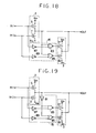
- Fig. 10 is shown an inverter circuit in accordance with the sixth embodiment of the present invention.
- a special feature of the circuit is that there is provided, for the output terminal OUT, a third inverting unit 3' that has the same configuration and mechanism as the second inverting unit 3, in parallel with the unit 3, the inversion operations of the third inverting unit 3' and the second inverting unit 3 are controlled by the control unit 15 based on the output potential, to vary the driving capability of the inverter circuit as a whole in three stages.
- the control unit 15 consists of a NOT gate, NAND gates, and NOR gates.
- the NAND gates 49 and 53 and the NOR gates 51 and 55 have one ends of their respective input terminals connected to the output terminal OUT, and the other ends of their respective input terminals connected to the input terminal IN via the NOT gate 47.
- the output terminal of the NAND gate 49 is connected to the gate terminal of the fourth PMOS transistor 17, and the output terminal of the NOR gate 51 is connected to the gate terminal of the fourth NMOS transistor 19.
- the output terminal of the NAND gate 53 is connected to the gate terminal of a fifth P-channel MOS type transistor 17' that constitutes a third inverting unit 3', and the output terminal of the NOR gate 55 is connected to a fifth N-channel MOS type transistor 19'.
- the inverter circuit in this embodiment has the input and output characteristics as shown in Fig. 11, and it is possible to obtain the same effects as in the inverter circuit described in the third embodiment.
- Fig. 12 there is shown an inverter circuit in accordance with a seventh embodiment of the present invention.
- the control unit 15 that has an EXCLUSIVE-OR gate and an EXCLUSIVE-NOR gate that have different threshold voltages for the two input terminals, controls the operation of the second inverting unit 3, based on the output potential. With this, it is arranged that the fall and rise of the output potential is to take place slowly, by reducing the driving capability of the inverter circuit in the vicinity of potential V or potential V DD of the output potential.
- the control unit 15 consists of a NOT gate, an EXCLUSIVE-OR gate (called “EX.OR gate” hereinafter), an EXCLUSIVE-NOR gate (called “EX.NOR gate” hereinafter), a NAND gate, and a NOR gate.
- EX.OR gate an EXCLUSIVE-OR gate
- EX.NOR gate an EXCLUSIVE-NOR gate
- NAND gate a NAND gate
- NOR gate NOR gate
- the other ends of the respective input terminals of the NAND gate 63 and the NOR gate 65 are connected to the input terminal IN via the NOT gate 57, the output terminal of the NAND gate 63 is connected to the gate terminal of the fourth PMOS transistor 17, and the output terminal of the NOR gate 65 is connected to the gate terminal of the fourth NMOS transistor 19. Further, the components with identical symbols as in Fig. 5 indicate the identical items and their description will be omitted.
- the second inverting unit 3 becomes high impedance state, so that the output potential falls slowly. Further, in the rise operation of the output potential, analogous to the fall operation, only when the output potential lies between potential V t1 and potential V t2 , the driving capability of the inverter circuit as a whole is increased. Accordingly, in the inverter circuit of the present embodiment, there are obtained the input and output characteristics as shown in Fig. 13, and effects similar to the inverter circuit explained in the third embodiment can be obtained.
- Fig. 14 is shown an inverter circuit in accordance with an eighth embodiment of the present invention.
- a special feature of the circuit is that, similar to the second embodiment, there is provided in the first half of the second inverting unit 3 a control unit 15 that controls the operation of the second inverting unit 3 based on the output potential.
- the output potential is first dropped or raised rapidly by increasing the driving capability of the inverter circuit as a whole, and the output potential is made to fall or rise slowly by decreasing the driving capability for the in-between.
- the control unit 15 consists of two NOT gates, a NAND gate and a NOR gate.
- the NAND gate 67 and the NOR gate 69 have one ends of their respective input terminals connected via the NOT gate 71 to the input terminal IN, and the other ends of their respective input terminals are connected via the NOT gate 73 to the output terminal OUT.
- the output terminal of the NAND gate 67 is connected to the gate terminal of the fourth PMOS transistor 17, and the output terminal of the NOR gate 69 is connected to the gate terminal of the fourth NMOS transistor 19.
- the components with identical symbols as in Fig. 5 indicate the identical items and their description is omitted.
- Fig. 16 is shown an inverter circuit in accordance.-with a ninth embodiment of the present invention.
- the control unit l5. is formed by a circuit which is different from the circuit shown in the eighth embodiment, and the control on the operation of the second inverting unit 3 is arranged to be carried out in a way similar to the eighth embodiment.
- the control unit 15 consists of NOT gates, a NAND gate, and a NOR gate.
- One ends of the respective input terminals of the NOR gate 73 and the NAND gate 75 are connected to the input terminal IN of the inverter circuit, and the other ends of their respective input terminals are connected to the output terminal OUT of the inverter circuit.
- the output terminal of the NOR gate 73 is connected via the NOT gate 77 to the gate terminal of the fourth PMOS transistor 17, and the output terminal of the NAND gate 75 is connected via the NOT gate 79 to the gate terminal of the fourth NMOS transistor 19.
- the components with identical symbols as in Fig. 5 indicate the identical items and their description is omitted.
- Fig. 17 is shown an inverter circuit in accordance with a tenth embodiment of the present invention.
- the input terminals of the NAND gate 43 and the NOR gate 45 that are not connected on the side of the input terminal IN of the buffer circuit are connected via the NOT gate 81 to the output terminal OUT of the buffer circuit, to construct the control unit 15 of the buffer circuit for this embodiment.
- the component with identical symbols as in Fig. 5 indicate the identical items and their description was omitted.
- FIG. 18 there is shown an inverter circuit in accordance with an eleventh embodiment of the present invention.
- a special feature of the circuit is that it is arranged to render the output terminal OUT a high impedance state by means of the signal states of the two input terminals that are provided in the inverter circuit.
- the gate terminal of the first PMOS transistor 5 that constitutes the first. inverting unit is connected to the input terminal IN 1
- the gate terminal of the first NMOS transistor 7 is connected to the input terminal IN 2
- the control unit 15 is constructed by NOT gates, a NAND gate, and a NOR gate, and one end of the input terminals of the NAND gate 83 is connected via the NOT gate 87 to the input terminal IN 1 of the inverter circuit, and the other end of its input terminals is connected to the output terminal OUT of the inverter circuit, and its output terminal is connected to the gate terminal of the fourth PMOS transistor 17.
- the NOR gate 85 has one of its input terminals connected via the NOT gate 89 to the input terminal IN 2 of the inverter circuit, the other end of the input terminals connected to the output terminal OUT of the inverter circuit, and its output terminal is connected to the gate terminal of the fourth N M OS transistor 19.
- the components with symbols identical to those in Fig. 5 indicate the identical items and their description was omitted.
- NOR gate 85 there is input a high level signal via the NOT gate 89, a low level signal is supplied from the output terminal of the NOR gate 85 to the gate terminal of the fourth NMOS transistor 19, and the fourth NMOS transistor 19 becomes turned off.
- Fig. 19 there is shown an inverter circuit in accordance with a twelfth embodiment of the present invention.
- a special feature of the circuit is that, in the control unit 15 in Fig. 18, the input terminals of the NAND gate 83 and the NOR gate 85, on the side that are not connected to the NOT gates 87 and 89, are connected via the NOT gate 91 to the output terminal OUT, to construct the control unit 15 for the inverter circuit for this embodiment.
- the inverter circuit of the present embodiment possesses input and output characteristics similar to those shown in Fig. 15, and is possible to obtain effects that are similar to those of the eighth embodiment.
- the components with identical symbols as in Fig. 18 indicate the identical items and their description was omitted.
- the transient current that arises at the time of charging or discharging of the load that is connected to the output terminal is suppressed by controlling the driving capability of the output circuit device in response to the output potential. Therefore, it is possible to suppress the overshoot and the undershoot phenomena in the output potential, which permits to improve the stability of the output potential.
Abstract
Description
- The present invention relates to an output circuit device, more particularly to an output circuit device which can realize stabilization of the output potential and the power supply potential.
- In the recent semiconductor devices, there has been pushed increases in the degree of integration and density to reduce the size of the chip, as well as there is observed a tendency of increasing the driving capability of transistors to make their operation fast.
- In order to reduce the chip size, it is necessary to make the width of the wirings formed by aluminum or the like small. By the reduction in the width of the wiring, the inductive load that exists in the wiring, namely, inductance, will have to be increased. Further, when the current driving capability is increased by increasing the size of the transistor, there will be generated problems that are caused by the increase in the inductive load of the wiring. This problem will now be described by making reference to Figs. 1 and 2.
- Figure 1 shows an example of configuration of a general inverter circuit that takes into account of the inductance components of the wirings for the power supply and the output. It consists of a P-channel MOS transistor (PMOS transistor) 101 and an N-channel MOS transistor (NMOS transistor) 103. The source terminal of the
PMOS transistor 101 is connected to a high level voltage source V that supplies a potential VDD via aninductance 105 that exists in a power supply wiring made of aluminum, and the source terminal of theNMOS transistor 103 is connected to a low level voltage source VSS that supplies a potential VSS (normally OV) via aninductance 107 that exists in a power supply wiring made of aluminum. Further, thePMOS transistor 101 and theNMOS transistor 103 have both of their gate terminals connected to the input terminal IN that inputs a signal to be inverted, and at the same time, their respective drain terminals are connected to the output terminal OUT via aninductance 109 that exists in the output wiring made of aluminum, and the output terminal OUT is connected to aload capacitor 111. - When a low level (potential VSS) signal is input to the input terminal IN, the
PMOS transistor 101 will become on-state and theNMOS transistor 103 will become off-state. Then, a current flows into theload capacitor 111 from the high level voltage source VDD via thePMOS transistor 101, bringing the output terminal OUT to the high level (potential VDD). On the contrary, when a high level signal (potential VDD) is input to the input terminal IN, thePMOS transistor 101 will be brought to off-state and theNMOS transistor 103 to on-state. Then, charge accumulated in the load capacitor flows into the low level voltage source VSS via theNMOS transistor 103, bringing the output terminal OUT to low level (potential VSS). Therefore, by the operation described above, there will be output from the output terminal OUT a signal which is the inversion of the signal that was input to the input terminal IN. - Now, in an inverter circuit with the above configuration, when the current driving capability of the transistors is enhanced by increasing the transistor size, in order to have a quickly inverted output potential, the on-resistance of the transistors become small, and there will be formed, between the high level voltage source VDD and the load capacitor lll, or between the low level voltage source VSS and the
load capacitor 111, a resonance circuit that consists of the load capacitor and the inductance that exists in the power supply wiring and the output wiring. Then, as shown in Fig. 2, when the input potential changes from potential VSS to potential VDD, theNMOS transistor 103 becomes on-state, and the output potential drops from potential VDD to potential VSS due to the rapid flow of change that was accumulated in theload capacitor 111 to the low level voltage source VSS, a transient current flows in the vicinity of potential VSS, giving rise to the so-called undershoot phenomenon. On the constrary, when the output potential is raised from potential VSS to potential VDD by the rapid charging due to flow of a current to theload capacitor 111 from the high level voltage source VDD, a transient current flows in the vicinity of potential VDD, giving rise to the so-called overshoot phenomenon. - As a result, the output potential varies temporarily immediately after it is inverted, giving rise to a problem of transmitting signals at erroneous potentials. Furthermore, it causes variations in the high level voltage source VDD and the low level voltage source VSS, which leads to a fear of generating malfunctions in the circuit through variations in the input and output levels of the other elements that are connected to the same power supply wiring.
- An object of the present invention is to provide an output circuit device which makes it possible to improve the stability in the output potential and the power supply potential.
- Another object of the present invention is to provide an output circuit device which is capable of suppressing the overshoot and the undershoot phenomena in the output potential.
- Another object of the present invention is to provide an output circuit device which can suppress the transient current that may be generated during charging or discharging of a load that is connected to the output terminal, by controlling the driving capability of the output circuit device in response to the output potential.
- A feature of the present invention exists in that in an output circuit device there are provided a first circuit which outputs an input signal by inverting it, a capacitive load which charges or discharges the output signal from the first circuit, and a second circuit which is connected to the first circuit for varying the rate of charging or discharging of the capacitive load in response to the potential of the output signal. The first circuit means has a first type MOS transistor and a second type MOS transistor that are connected in parallel to each other, the source of the first type MOS transistor is connected to a first power supply, the source of the second type MOS transistor is connected to a second power supply, and the gates of the first and the second type MOS transistors are connected in parallel to the input terminal.
- Further, the second circuit means has at least a first type MOS transistor and a second type MOS transistor that are connected in parallel to each other, as well as it is connected between the output side of the first circuit means and the output terminal, with the source of the first type MOS transistor of the second circuit means connected to the first power supply, the source of the second type MOS transistor of the same circuit means connected to the second power supply, and the first and the second MOS transistors having a first threshold voltage level.
- These and other objects, features and advantages of the present invention will be more apparent from the following description of the preferred embodiments, taken in conjunction with the accompanying drawings.
-
- Fig. 1 is a circuit diagram for a prior art inverter circuit;
- Fig. 2 is a graph for showing the input and output characteristics of the inverter circuit shown in Fig. 1;
- Fig. 3 is a circuit diagram for a first embodiment of the inverter circuit in accordance with the present invention;
- Fig. 4 is a graph for showing the input and output characteristics of the inverter circuit shown in Fig. 3;
- Fig. 5 is a circuit diagram for a second embodiment of the inverter circuit in accordance with the present invention;
- Fig. 6 is a graph for showing the input and output characteristics of the inverter circuit shown in Fig. 5;
- Fig. 7 is a circuit diagram for a third embodiment of the inverter circuit in accordance with the present invention;
- Fig. 8 is a circuit diagram for a fourth embodiment of the inverter circuit in accordance with the present invention;
- Fig. 9 is a circuit diagram for the buffer circuit for a fifth embodiment of the present invention;
- Fig. 10 is a circuit diagram for a sixth embodiment of the inverter circuit in accordance with the present invention;
- Fig. 11 is a graph for showing the input and output characteristics of the inverter circuit shown in Fig. 10;
- Fig. 12 is a circuit diagram for a seventh embodiment of the inverter circuit in accordance with the present invention;
- Fig. 13 is a graph for showing the input and output characteristics of the inverter circuit shown in Fig. 12;
- Fig. 14 is a circuit diagram for an eighth embodiment of the inverter circuit in accordance with the present invention;
- Fig. 15 is a graph for showing the input and output characteristics of the inverter circuit shown in Fig. 14;
- Fig. 16 is a circuit diagram for a ninth embodiment of the inverter circuit in accordance with the present invention;
- Fig. 17 is a circuit diagram for the buffer circuit for a tenth embodiment of the present invention;
- Fig. 18 is a circuit diagram for an eleventh embodiment of the inverter circuit in accordance with the present invention; and
- Fig. 19 is a circuit diagram for a twelfth embodiment of the inverter circuit in accordance with the present invention.
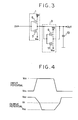
- Referring to Fig. 3, an inverter circuit embodying the present invention is shown. The inverter circuit comprises a
first inverting unit 1 which inverts a signal that is input from the input terminal IN, a second invertingunit 3 driving of which is controlled by the output potential, and which assists the inverting operation that is performed by thefirst inverting unit 1, and aload capacitor 13 which is connected to the output terminal OUT. - The first inverting
unit 1 consists of a first P-channel MOS type transistor (which will be called "first PMOS transistor" hereinafter) 5 and a first N-channel MOS type transistor (which will be called "first NMOS transistor" hereinafter) 7. - The
first PMOS transistor 5 and thefirst NMOS transistor 7 have their respective gate terminals connected to the input terminal IN to which is input a signal to be inverted, and their respective drain terminals connected to the output terminal OUT which outputs the signal that is inverted. Further, the source terminal of thefirst PMOS transistor 5 is connected to a high level voltage source VDD that supplies a potential VDD, and the source terminal of thefirst NMOS transistor 7 is connected to a low level voltage source V that supplies a potential VSS (normally OV). - The second inverting
unit 3 consists of a second N-channel MOS type transistor (called "second NMOS transistor" hereinafter) 9 and a second P-channel MOS type transistor (called "second PMOS transistor" hereinafter) 11. - The second NMOS transistor 9 and the
second PMOS transistor 11 have both of their respective gate terminals and drain terminals connected to the output terminal OUT, the source terminal of the second NMOS transistor 9 is connected to the high level voltage source VDD' and the source terminal of thesecond PMOS transistor 11 is connected to the low level voltage source VSS. In addition, the output terminal is connected to theload capacitor 13. - Next, the operation of the first embodiment of the present invention with the above configuration will be described by making reference to Fig. 4.
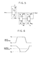
- First, the case in which the input potential of the input terminal IN is changed from low level (potential VSS) to high level (potential VDD), as shown in Fig. 4 will be described. It should be noted that prior to this change, the
first PMOS transistor 5 and the second NMOS transistor 9 were in on-state, thefirst NMOS transistor 7 and thesecond PMOS transistor 11 were in off-state, theload capacitor 13 is charged by the feeding from the high level voltage source VDD' and the output potential was in high level (potential VDD). - When the high level signal input to the input terminal IN is supplied to the respective gate terminals of the
first PMOS transistor 5 and thefirst NMOS transistor 7, thefirst PMOS transistor 5 is shifted from on-state to off-state while thefirst NMOS transistor 7 is shifted from off-state to on-state. By the shift of thefirst NMOS transistor 7 to on-state, charge, that was accumulated in theload capacitor 13 that is connected to the output terminal OUT during the time when the output terminal OUT was on high level, flows into the low level voltage source VSS via thefirst NMOS transistor 7, causing the output potential to start dropping as shown in Fig. 4. When the output potential drops to the threshold voltage Vt for the second NMOS transistor 9 and thesecond PMOS transistor 11, the second NMOS transistor 9 is shifted from on-state to off-state, while thesecond PMOS transistor 11 is shifted from off-state to on-state. Because of this, a part of the charge that has been accumulated in theload capacitor 13 flows into the low level voltage source VSS via thesecond PMOS transistor 11. - In other words, when the input potential becomes the state of high level, charge that was accumulated in the
load capacitor 13 is discharged via the first NMOS transistor alone, so that the output potential drops relatively slowly from potential VDD to potential Vt. From potential Vt to potential VSS' charge is discharged via both of thefirst NMOS transistor 7 and thesecond PMOS transistor 11, which means that the driving capability of the inverter circuit as a whole is increased, so that the output potential drops rapidly as shown in Fig. 4. - Because of this, at the point in time when the second inverting
unit 3 is to be operated, the output potential is dropped to potential Vt by a partial discharge of the charge that was accumulated in theload capacitor 13. Therefore, the transient current is small compared with the case of discharging the charge accumulated in the load capacitor in one step so that the undershoot phenomenon can be suppressed. - Next, the case in which the signal that is input to the input terminal IN is changed from high level to low level, while the output terminal OUT is in the low level state, will be described. When this low level signal is supplied to the gate terminals of the
first PMOS transistor 5 and thefirst NMOS transistor 7, thefirst PMOS transistor 5 is shifted from off-state to on-state and thefirst NMOS transistor 7 is shifted from on-state to off-state. By the change to the on-state of thefirst PMOS transistor 5, a current flows from the high level voltage source V to theload capacitor 13 via thefirst PMOS transistor 5 which results in a start of rise in the output potential due to charging of theload capacitor 13, as shown in Fig. 4. When the output potential is raised to the threshold voltage Vt of the second NMOS transistor 9 and thesecond PMOS transistor 11, the second NMOS transistor 9 is changed from off-state to on-state and thesecond PMOS transistor 11 is changed from on-state to off-state. Then, a part of the charge that is accumulated in theload capacitor 13 is supplied from the high level voltage source VDD via the second NMOS transistor 9. - Namely, when the input potential changes from high level to low level state and the output potential changes from potential VSS to potential Vt, charge is supplied from the high level voltage source VDD to the
load capacitor 13 only through thefirst PMOS transistor 5 to charge the capacitor, resulting in a relatively slow rise in the output potential. During the rise of the output potential from potential Vt to potential VDD, charge is supplied from the high level voltage source VDD to theload capacitor 13 to charge it via both of thefirst PMOS transistor 5 and the second NMOS transistor 9, so that the output potential is raised rapidly as shown in Fig. 4. - Therefore, analogous to the case of the fall of the output potential, even if the output potential is raised rapidly by the operation of the
second inverting unit 3, the transient current is small compared with the case of raising the output potential from potential VSS to potential VDD in one step, because the output potential is already raised to potential V at the point in time when the second inverting unit 3.operates. Accordingly, the overshoot phenomenon can be suppressed. - In Fig. 5 is shown a second inverter circuit in accordance with the present invention. Its special feature is that in the inverter circuit shown in Fig. 3 there is provided a
control unit 15 that controls the operation of thesecond inverting unit 3 by means of the output potential, in the first half of thesecond inverting unit 3. It is to be noted that in the embodiments to be described in the following, the load capacitor that is connected to the output terminal OUT will be omitted from the figure. - The
control unit 15 consists of a CMOS circuit formed by a third P-channel MOS type transistor (called "third PMOS transistor" hereinafter) 21 and a third N-channel MOS type transistor (called "third NMOS transistor" hereinafter) 23. - The
third PMOS transistor 21 and thethird NMOS transistor 23 have their respective gate terminals connected to the output terminal OUT, and their drain terminals connected to each other, and the source terminal of thethird PMOS transistor 21 is connected to the high level voltage source VDD while the source terminal of thethird NMOS transistor 23 is connected to the low level voltage source VSS' - The
second inverting unit 3 consists of a CMOS circuit formed by a fourth P-channel MOS type transistor (called "fourth PMOS transistor" hereinafter) 17 and a fourth N-channel MOS type transistor (called "fourth NMOS transistor" hereinafter) 19. - The
fourth PMOS transistor 17 and thefourth NMOS transistor 19 have their respective gate terminals connected to the drain terminals of thethird PMOS transistor 21 and thethird NMOS transistor 23, and their respective drain terminals connected to the output terminal OUT. The source terminal of thefourth PMOS transistor 17 is connected to the high level voltage source VDD and the source terminal of thefourth NMOS transistor 19 is connected to the low level voltage source VSS. Further, components.with identical symbols as in Fig. 3 indicate the identical items and their description will be omitted. - With such a configuration, the
control unit 15 carries out the inversion operation by the means of threshold voltage V for thethird PMOS transistor 21 and thethird NMOS transistor 23, and also carries out the control of the operation of thesecond inverting unit 3, so that thesecond inverting unit 3 will operate in the same way as in the first embodiment. Therefore, the fall of the output potential from potential VDD to potential Vt is carried out slow, whereas the drop from potential Vt to potential VSS is rapid. Further, in the rise of the output potential, the increase from potential VSS to potential Vt is carried out gently, whereas the rise from potential Vt to potential VDD is carried out rapidly, as shown in Fig. 6. - Accordingly, with such a configuration, similar effects as in the first embodiment can be obtained. In addition, the source terminal of the
fourth PMOS transistor 17 of thesecond inverting unit 3 is connected to the high level voltage source VDD and the source terminal of thefourth NMOS transistor 19 of the same unit is connected to the low level voltage source VSS' so that thesecond inverting unit 3 can carry out a full swing operation between potential VSS and potential VDDo - It should be noted that in the first and second embodiments, the
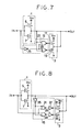
first inverting unit 1 and thesecond inverting unit 3 are turned on, at the time of inversion of the output potential, on the sides of potential that are mutually opposite with respect to the output potential. Because of this, to ensure the inversion operation, in the first embodiment, the driving capability of thefirst PMOS transistor 5 has to be chosen higher than the driving capability of thesecond PMOS transistor 11, and also, the driving capability of thefirst NMOS transistor 7 has to be chosen higher than the driving capability of the second NMOS transistor 9. Further, in the second embodiment, it is necessary to choose the driving capability of thefirst PMOS transistor 5 to be higher than the driving capability of thefourth NMOS transistor 19, as well as the driving capability of thefirst NMOS transistor 7 to be chosen higher than the driving capability of thefourth PMOS transistor 17. - In Fig. 7 is shown a third embodiment of the inverter circuit in accordance with the present invention. The special feature of the embodiment resides in that the
control unit 15 shown in the second embodiment is composed of aNOT gate 25, aNAND gate 27 and a NORgate 29, to prevent, in the inverter circuit shown in the first and the second embodiments, the simultaneous operation of thefirst inverting unit 1 and thesecond inverting unit 3 on the opposite potential sides with respect to the output potential. - The NOT gate has its input terminal connected to the input terminal IN of the inverter circuit, and its output terminal is connected to one end of the input terminals of the
NAND gate 27 that has a two-input terminal, as well as to one end of the input terminals of the NORgate 29 that has a two-input terminal. The other end of the input terminals of theNAND gate 27 and the NORgate 29 is connected to the output terminal OUT, and the output terminal of theNAND gate 27 is connected to the gate terminal of thefourth PMOS transistor 17, while the output terminal of the NORgate 29 is connected to the gate terminal of thefourth NMOS transistor 19. - With such a configuration, it is arranged that when the output potential exceeds the threshold potential for the
NAND gate 27 and the NORgate 29, thesecond inverting unit 3 of the inverter circuit is activated so that the driving capability of the inverter circuit as a whole will become increased. Accordingly, its output potential will possess characteristics similar to what was shown in Fig. 4. Further, during the period from inversion of the input potential to the attainment of the threshold voltage Vt for theNAND gate 27 and the NORgate 29, thesecond inverting unit 3 is in the state of high impedance, and thefirst inverting unit 1 alone is operated. Therefore, thefirst inverting unit 1 and thesecond inverting unit 3 will never be turned on simultaneously on the opposite potential sides with respect to the output potential. It is to be noted that the components with identical symbols as in Fig. 5 indicate the identical items and their description was omitted. - In Fig. 8 is shown an inverter circuit for a fourth embodiment of the present invention. In this inverter circuit a
control unit 15 for controlling thesecond inverting unit 3 is provided in the first half of thesecond inverting unit 3, analogous to the inverter circuit shown in Fig. 7. - The
control unit 15 consists of a NOT gate, a NAND gate and a NOR gate. The NORgate 31 and theNAND gate 33 have one ends of their respective input terminals connected to the input terminal IN, and have the other ends of their respective input terminals connected to the output terminal OUT via theNOT gate 35. The output terminal of the NORgate 31 is connected via theNOT gate 37 to the gate terminal of thefourth PMOS transistor 17, and the output terminal of theNAND gate 33 is connected via theNOT gate 39 to the gate terminal of thefourth NMOS transistor 19. Further, the components with identical symbols as in Fig. 5 indicate the identical items and their description was omitted. - With such a configuration, it is possible to obtain the input and output characteristics also similar to those of Fig. 7, and hence similar effects.
- In Fig. 9 is shown a buffer circuit in accordance with the fifth embodiment of the present invention. A special feature of the circuit exists in that the buffer operation is carried out by connecting a
NOT gate 41 between the input terminal IN and thefirst inverting unit 1, and the overshoot and the undershoot phenomena in the rise and fall operations, respectively, of the output potential is suppressed by providinga-control unit 15 in the first half of thesecond inverting unit 3. - The
control unit 15 consists of a NAND gate and a NOR gate. ANAND gate 43 and a NORgate 45 have one ends of their respective input terminals connected to the input terminal IN, and the other ends of their respective input terminals connected to the output terminal OUT. The output terminal of theNAND gate 43 is connected to the gate terminal of thefourth PMOS transistor 17, and the output terminal of the NORgate 45 is connected to the gate terminal of thefourth NMOS transistor 19. Components with identical symbols with those of Fig. 5 indicate the identical items and their description was omitted. - With such a configuration, the
second inverting unit 3 starts to operate when the output voltage exceeds the threshold voltage Vt for theNAND gate 43 and the NORgate 45, to increase the driving capability of the buffer circuit as a whole, and the rise and fall operations of the output potential are divided in two steps similar to the inverter circuit shown in Fig. 7. - In Fig. 10 is shown an inverter circuit in accordance with the sixth embodiment of the present invention. A special feature of the circuit is that there is provided, for the output terminal OUT, a third inverting unit 3' that has the same configuration and mechanism as the
second inverting unit 3, in parallel with theunit 3, the inversion operations of the third inverting unit 3' and thesecond inverting unit 3 are controlled by thecontrol unit 15 based on the output potential, to vary the driving capability of the inverter circuit as a whole in three stages. - The
control unit 15 consists of a NOT gate, NAND gates, and NOR gates. TheNAND gates gates 51 and 55 have one ends of their respective input terminals connected to the output terminal OUT, and the other ends of their respective input terminals connected to the input terminal IN via theNOT gate 47. The output terminal of theNAND gate 49 is connected to the gate terminal of thefourth PMOS transistor 17, and the output terminal of the NOR gate 51 is connected to the gate terminal of thefourth NMOS transistor 19. Further, the output terminal of theNAND gate 53 is connected to the gate terminal of a fifth P-channel MOS type transistor 17' that constitutes a third inverting unit 3', and the output terminal of the NORgate 55 is connected to a fifth N-channel MOS type transistor 19'. - With such a configuration, in the fall operation, for example, of the output potential, when the input potential changes from the low level to the high level, the
first inverting unit 1 operates first, and the output potential drops from potential VDD to the threshold voltage Vti for theNAND gate 53 and the NORgate 55, when the third inverting unit 3' begins to operate. When the output potential drops further to the threshold voltage Vt2 for theNAND gate 49 and the NOR gate 51, thesecond inverting unit 3 begins to operate. In this way, the driving capability of the inverter circuit is arranged to be increased successively. In a similar manner, in the rise operation of the output potential, too, the driving capability of the inverter circuit is increased successively. Accordingly, the inverter circuit in this embodiment has the input and output characteristics as shown in Fig. 11, and it is possible to obtain the same effects as in the inverter circuit described in the third embodiment. - In Fig. 12 there is shown an inverter circuit in accordance with a seventh embodiment of the present invention. A special feature of the circuit exists in that the
control unit 15 that has an EXCLUSIVE-OR gate and an EXCLUSIVE-NOR gate that have different threshold voltages for the two input terminals, controls the operation of thesecond inverting unit 3, based on the output potential. With this, it is arranged that the fall and rise of the output potential is to take place slowly, by reducing the driving capability of the inverter circuit in the vicinity of potential V or potential VDD of the output potential. - The
control unit 15 consists of a NOT gate, an EXCLUSIVE-OR gate (called "EX.OR gate" hereinafter), an EXCLUSIVE-NOR gate (called "EX.NOR gate" hereinafter), a NAND gate, and a NOR gate. The respective input terminals of theEX.OR gate 59 and the EX.NORgate 61, that have the threshold voltage of Vti and Vt2 for the two input terminals, respectively, are connected to the output terminal OUT, the output terminal of theEX.OR gate 59 is connected to one end of the input terminals of theNAND gate 63, and the output terminal of the EX.NORgate 61 is connected to one end of the input terminals of the NORgate 65. The other ends of the respective input terminals of theNAND gate 63 and the NORgate 65 are connected to the input terminal IN via theNOT gate 57, the output terminal of theNAND gate 63 is connected to the gate terminal of thefourth PMOS transistor 17, and the output terminal of the NORgate 65 is connected to the gate terminal of thefourth NMOS transistor 19. Further, the components with identical symbols as in Fig. 5 indicate the identical items and their description will be omitted. - IN such a configuration, in the fall operation, for example, of the output potential, when the output potential lies between potentials Vti and Vt2, a low level signal is output from the EX.NOR
gate 61 to the NORgate 65, the NORgate 65 supplies, upon receipt of the low level signal, a high level signal to thefourth NMOS transistor 19 of thesecond inverting unit 3, and the fourth NMOS transistor becomes turned on. Therefore, the driving capability of the inverter circuit as a whole is increased, and the output potential drops rapidly. When the output potential lies between potentials VDD and Vti and between potentials Vt2 and VSS, thefirst NMOS transistor 7 alone of thefirst inverting unit 1 becomes turned on. Thesecond inverting unit 3 becomes high impedance state, so that the output potential falls slowly. Further, in the rise operation of the output potential, analogous to the fall operation, only when the output potential lies between potential Vt1 and potential Vt2, the driving capability of the inverter circuit as a whole is increased. Accordingly, in the inverter circuit of the present embodiment, there are obtained the input and output characteristics as shown in Fig. 13, and effects similar to the inverter circuit explained in the third embodiment can be obtained. - In Fig. 14 is shown an inverter circuit in accordance with an eighth embodiment of the present invention. A special feature of the circuit is that, similar to the second embodiment, there is provided in the first half of the second inverting unit 3 a
control unit 15 that controls the operation of thesecond inverting unit 3 based on the output potential. In the rise and the fall operations of the output potential, contrary to the input and output characteristics of the third embodiment, the output potential is first dropped or raised rapidly by increasing the driving capability of the inverter circuit as a whole, and the output potential is made to fall or rise slowly by decreasing the driving capability for the in-between. - The
control unit 15 consists of two NOT gates, a NAND gate and a NOR gate. TheNAND gate 67 and the NORgate 69 have one ends of their respective input terminals connected via theNOT gate 71 to the input terminal IN, and the other ends of their respective input terminals are connected via theNOT gate 73 to the output terminal OUT. Further, the output terminal of theNAND gate 67 is connected to the gate terminal of thefourth PMOS transistor 17, and the output terminal of the NORgate 69 is connected to the gate terminal of thefourth NMOS transistor 19. In addition, the components with identical symbols as in Fig. 5 indicate the identical items and their description is omitted. - With such a configuration, in the fall operation, for example, of the output potential, when the input potential changes from low-level to high level, the first NMOS transistor is turned on. Until the output potential drops to the threshold voltage Vt of the
NOT gate 73, low level signals will be input to both of the input terminals of the NORgate 69, so that the NOR gate supplies high level output signals to thefourth NMOS transistor 19 which will also become turned on. Accordingly, the driving capability of the inverter circuit as a whole is increased, and the output potential is lowered rapidly. - When the output potential drops to potential Vt, there will be input high level signals to the input terminal of the NOR
gate 69 that is connected via theNOT gate 73 to the output terminal OUT. Therefore, low level output signals will be supplied from the NORgate 69 to thefourth NMOS transistor 19, thefourth NMOS transistor 19 is turned off reducing the driving capability of the inverter circuit as a whole, leading to a slow drop of the output potential. In addition, in the rise operation of the output potential, similar to the fall operation, the driving capability of the inverter circuit as a whole is decreased when the output potential exceeds potential Vt, and the input and output characteristics as shown in Fig. 15 will be obtained. - In the input and output characteristics as shown in Fig. 15, although a large transient current flows in the beginning, after the output potential crosses potential Vt, the driving capability is weakened and the transient current is suppressed. Because of this, when the output potential is in the vicinity of potential VDD or potential VSS, the transient current is reduced considerably so that it becomes possible to suppress the overshoot or undershoot phenomenon. Moreover, for elements such as a CMOS circuit that is operated based on the level of the input signal, it is possible to shorten the transmission time, as the output potential is lowered rapidly in the beginning.
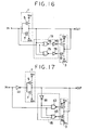
- In Fig. 16 is shown an inverter circuit in accordance.-with a ninth embodiment of the present invention. In the ninth embodiment, the control unit l5.is formed by a circuit which is different from the circuit shown in the eighth embodiment, and the control on the operation of the
second inverting unit 3 is arranged to be carried out in a way similar to the eighth embodiment. - The
control unit 15 consists of NOT gates, a NAND gate, and a NOR gate. One ends of the respective input terminals of the NORgate 73 and theNAND gate 75 are connected to the input terminal IN of the inverter circuit, and the other ends of their respective input terminals are connected to the output terminal OUT of the inverter circuit. Further, the output terminal of the NORgate 73 is connected via theNOT gate 77 to the gate terminal of thefourth PMOS transistor 17, and the output terminal of theNAND gate 75 is connected via theNOT gate 79 to the gate terminal of thefourth NMOS transistor 19. In addition, the components with identical symbols as in Fig. 5 indicate the identical items and their description is omitted. - With such a configuration, it is possible to obtain the input and output characteristics that are similar to those shown in Fig. 15, and also the effects that are similar to the eighth embodiment.
- In Fig. 17 is shown an inverter circuit in accordance with a tenth embodiment of the present invention. In this embodiment, in the
control unit 15 of the buffer circuit of the fourth embodiment shown in Fig. 9, the input terminals of theNAND gate 43 and the NORgate 45 that are not connected on the side of the input terminal IN of the buffer circuit are connected via theNOT gate 81 to the output terminal OUT of the buffer circuit, to construct thecontrol unit 15 of the buffer circuit for this embodiment. In addition, the component with identical symbols as in Fig. 5 indicate the identical items and their description was omitted. - With such a configuration, in the rise operation, for example, of the output potential, until the output potential arrives at the threshold voltage- V of the
NOT gate 81, thefirst PMOS transistor 5 and thefourth PMOS transistor 17 are in on-state so that the output potential is raised rapidly by the increase in the driving capability of the inverter circuit as a whole. When the output potential becomes potential Vt, thefourth PMOS transistor 17 becomes turned off so that the output potential is raised slowly because of the weakening of the driving capability. Further, in the fall operation of the output potential, analogous to the rise operation, the output potential falls rapidly in the beginning, but the output potential falls slowly when the output potential becomes potential Vt. Accordingly, effects similar to the eighth embodiment can be obtained. - In Fig. 18 there is shown an inverter circuit in accordance with an eleventh embodiment of the present invention. A special feature of the circuit is that it is arranged to render the output terminal OUT a high impedance state by means of the signal states of the two input terminals that are provided in the inverter circuit.
- In Fig. 18, the gate terminal of the
first PMOS transistor 5 that constitutes the first. inverting unit is connected to the input terminal IN1, and the gate terminal of thefirst NMOS transistor 7 is connected to the input terminal IN2. Thecontrol unit 15 is constructed by NOT gates, a NAND gate, and a NOR gate, and one end of the input terminals of theNAND gate 83 is connected via theNOT gate 87 to the input terminal IN1 of the inverter circuit, and the other end of its input terminals is connected to the output terminal OUT of the inverter circuit, and its output terminal is connected to the gate terminal of thefourth PMOS transistor 17. The NORgate 85 has one of its input terminals connected via theNOT gate 89 to the input terminal IN2 of the inverter circuit, the other end of the input terminals connected to the output terminal OUT of the inverter circuit, and its output terminal is connected to the gate terminal of the fourth NMOS transistor 19. In addition, the components with symbols identical to those in Fig. 5 indicate the identical items and their description was omitted. - With such a configuration, when a high level signal is input to the input terminal IN1 and a low level signal is input to the input terminal IN2, both of the
first PMOS transistor 5 and thefirst NMOS transistor 7 becomes turned off. Further, to one of the input terminals of theNAND gate 83 is input a low level signal via theNOT gate 87, and a high level signal is supplied from the output terminal of theNAND gate 83 to the gate terminal of thefourth PMOS transistor 17, and thefourth PMOS transistor 17 becomes turned off. Further, to one of the input terminals of the NORgate 85 there is input a high level signal via theNOT gate 89, a low level signal is supplied from the output terminal of the NORgate 85 to the gate terminal of thefourth NMOS transistor 19, and thefourth NMOS transistor 19 becomes turned off. - Accordingly, when a high level signal is input to the input terminal IN, and a low level signal is input to the input terminal IN2, regardless of the state of the output potential, the output terminal OUT becomes a state of high impedance. Further, when signals of the same phase are input to both input terminals of INland IN2, there are obtained input and output characteristics that are similar to those of the inverter circuit of the third embodiment shown in Fig. 7, and also the same effects as for the third embodiment.
- In Fig. 19 there is shown an inverter circuit in accordance with a twelfth embodiment of the present invention. A special feature of the circuit is that, in the
control unit 15 in Fig. 18, the input terminals of theNAND gate 83 and the NORgate 85, on the side that are not connected to theNOT gates NOT gate 91 to the output terminal OUT, to construct thecontrol unit 15 for the inverter circuit for this embodiment. Analogous to the inverter circuit shown in Fig. 18, irrespective of the state of the output potential, it is arranged to be able to render the output terminal OUT to be a state of high impedance. Moreover, the inverter circuit of the present embodiment possesses input and output characteristics similar to those shown in Fig. 15, and is possible to obtain effects that are similar to those of the eighth embodiment. In addition, the components with identical symbols as in Fig. 18 indicate the identical items and their description was omitted. - In summary, according to the present invention, the transient current that arises at the time of charging or discharging of the load that is connected to the output terminal is suppressed by controlling the driving capability of the output circuit device in response to the output potential. Therefore, it is possible to suppress the overshoot and the undershoot phenomena in the output potential, which permits to improve the stability of the output potential.
- Various modifications will become possible for those skilled in the art after receiving the teachings of the present disclosure without departing from the scope thereof.
Claims (19)
Applications Claiming Priority (2)
| Application Number | Priority Date | Filing Date | Title |
|---|---|---|---|
| JP60177688A JPH0720060B2 (en) | 1985-08-14 | 1985-08-14 | Output circuit device |
| JP177688/85 | 1985-08-14 |
Publications (3)
| Publication Number | Publication Date |
|---|---|
| EP0212584A2 true EP0212584A2 (en) | 1987-03-04 |
| EP0212584A3 EP0212584A3 (en) | 1988-08-17 |
| EP0212584B1 EP0212584B1 (en) | 1993-11-18 |
Family
ID=16035366
Family Applications (1)
| Application Number | Title | Priority Date | Filing Date |
|---|---|---|---|
| EP86111280A Expired - Lifetime EP0212584B1 (en) | 1985-08-14 | 1986-08-14 | Output circuit device with stabilized potential |
Country Status (4)
| Country | Link |
|---|---|
| US (1) | US4779013A (en) |
| EP (1) | EP0212584B1 (en) |
| JP (1) | JPH0720060B2 (en) |
| DE (1) | DE3689296T2 (en) |
Cited By (11)
| Publication number | Priority date | Publication date | Assignee | Title |
|---|---|---|---|---|
| EP0284356A2 (en) * | 1987-03-23 | 1988-09-28 | Kabushiki Kaisha Toshiba | A data output circuit |
| EP0285068A2 (en) * | 1987-03-27 | 1988-10-05 | Kabushiki Kaisha Toshiba | Logic circuit |
| EP0303341A2 (en) * | 1987-08-13 | 1989-02-15 | Advanced Micro Devices, Inc. | Output buffer circuits |
| EP0346876A1 (en) * | 1988-06-17 | 1989-12-20 | Fujitsu Limited | Semiconductor integrated circuit having a CMOS inverter |
| EP0348894A2 (en) * | 1988-06-27 | 1990-01-03 | Nec Corporation | Output buffer circuit used for stable voltage source |
| WO1991009466A1 (en) * | 1989-12-20 | 1991-06-27 | Vlsi Technology, Inc. | Auto-delay gain circuit |
| EP0441317A1 (en) * | 1990-02-07 | 1991-08-14 | Kabushiki Kaisha Toshiba | Bi-CMOS logic gate circuits for low-voltage semiconductor integrated circuits |
| GB2242587A (en) * | 1990-02-01 | 1991-10-02 | Mole Valley Systems Ltd | Switching circuits |
| EP0456354A2 (en) * | 1990-04-25 | 1991-11-13 | AT&T Corp. | Integrated circuit buffer with improved drive capability |
| EP0511643A1 (en) * | 1991-04-30 | 1992-11-04 | Kabushiki Kaisha Toshiba | Output buffer circuit |
| EP1014583A1 (en) * | 1998-12-17 | 2000-06-28 | United Memories, Inc. | Multi-stage data anticipation driver and method for an integrated circuit device |
Families Citing this family (90)
| Publication number | Priority date | Publication date | Assignee | Title |
|---|---|---|---|---|
| US4829199A (en) * | 1987-07-13 | 1989-05-09 | Ncr Corporation | Driver circuit providing load and time adaptive current |
| JPH0622649B2 (en) * | 1988-01-14 | 1994-03-30 | 株式会社テクノ菱和 | Air outlet unit for filters |
| NL8800075A (en) * | 1988-01-14 | 1989-08-01 | Philips Nv | HOT CARRIER STRESS FREE PUSH-PULL OUTPUT CIRCUIT. |
| US4880997A (en) * | 1988-08-18 | 1989-11-14 | Ncr Corporation | Low noise output buffer circuit |
| JPH0282713A (en) * | 1988-09-19 | 1990-03-23 | Fujitsu Ltd | Switching auxiliary circuit |
| JPH0777345B2 (en) * | 1988-11-04 | 1995-08-16 | 三菱電機株式会社 | Semiconductor device |
| US4906867A (en) * | 1988-11-09 | 1990-03-06 | Ncr Corporation | Buffer circuit with load sensitive transition control |
| JPH0666674B2 (en) * | 1988-11-21 | 1994-08-24 | 株式会社東芝 | Output circuit of semiconductor integrated circuit |
| JP2595074B2 (en) * | 1988-11-24 | 1997-03-26 | 三菱電機株式会社 | Semiconductor integrated circuit device |
| JP2788745B2 (en) * | 1988-12-28 | 1998-08-20 | 日本電気アイシーマイコンシステム株式会社 | Dynamic holding bus driver |
| US5010256A (en) * | 1989-02-21 | 1991-04-23 | United Technologies Corporation | Gate output driver using slew-rate control |
| US5216294A (en) * | 1989-05-31 | 1993-06-01 | Samsung Electronics Co., Ltd. | Data output buffer using a junction field effect transistor |
| US4962345A (en) * | 1989-11-06 | 1990-10-09 | Ncr Corporation | Current limiting output driver |
| US5070259A (en) * | 1989-12-26 | 1991-12-03 | Linear Technology Corporation | Constant current, highspeed, auto-zeroed, CMOS comparator |
| JPH0435224A (en) * | 1990-05-28 | 1992-02-06 | Nec Corp | Semiconductor device |
| US5241221A (en) * | 1990-07-06 | 1993-08-31 | North American Philips Corp., Signetics Div. | CMOS driver circuit having reduced switching noise |
| IL95576A0 (en) * | 1990-09-04 | 1991-06-30 | Quick Tech Ltd | Controlled slew rate buffer |
| US5122690A (en) * | 1990-10-16 | 1992-06-16 | General Electric Company | Interface circuits including driver circuits with switching noise reduction |
| JPH04154212A (en) * | 1990-10-17 | 1992-05-27 | Mitsubishi Electric Corp | Output circuit for semiconductor memory device |
| JP2978302B2 (en) * | 1991-01-28 | 1999-11-15 | 三菱電機株式会社 | Output buffer circuit |
| US5194760A (en) * | 1991-12-23 | 1993-03-16 | Motorola, Inc. | Slew rate limited inductive load driver |
| JPH066195A (en) * | 1992-06-18 | 1994-01-14 | Mitsubishi Electric Corp | Output driver circuit |
| US5306965A (en) * | 1992-07-01 | 1994-04-26 | Hewlett-Packard Co. | Process compensating variable impedence I/O driver with feedback |
| DE4233850C1 (en) * | 1992-10-08 | 1994-06-23 | Itt Ind Gmbh Deutsche | Circuit arrangement for current setting of a monolithically integrated pad driver |
| US5444398A (en) * | 1992-12-17 | 1995-08-22 | Siemens Aktiengesellschaft | Decoded-source sense amplifier with special column select driver voltage |
| US5426376A (en) * | 1993-04-23 | 1995-06-20 | Vlsi Technology, Inc. | Noise isolated I/O buffer that uses two separate power supplies |
| US5751167A (en) * | 1993-08-16 | 1998-05-12 | Nec Corporation | CMOS output buffer circuit which converts CMOS logic signals to ECL logic signals and which discharges parasitic load capacitances |
| US5436584A (en) * | 1993-11-15 | 1995-07-25 | Intel Corporation | Noise suppressing circuit for VLSI |
| FR2716758B1 (en) * | 1994-02-28 | 1996-05-31 | Sgs Thomson Microelectronics | Bias circuit for transistor in a storage cell. |
| JP3190199B2 (en) * | 1994-03-16 | 2001-07-23 | 株式会社東芝 | In-phase signal output circuit, anti-phase signal output circuit, two-phase signal output circuit, and signal output circuit |
| JPH07307649A (en) * | 1994-05-13 | 1995-11-21 | Fujitsu Ltd | Electronic device |
| JP3442149B2 (en) * | 1994-07-28 | 2003-09-02 | 富士通株式会社 | Semiconductor circuit |
| US5486782A (en) * | 1994-09-27 | 1996-01-23 | International Business Machines Corporation | Transmission line output driver |
| JP2590758B2 (en) * | 1994-10-31 | 1997-03-12 | 日本電気株式会社 | Bus driver |
| EP0778966A4 (en) * | 1995-05-17 | 1998-10-28 | Motorola Inc | Low power regenerative feedback device and method |
| US5739715A (en) * | 1995-10-31 | 1998-04-14 | Hewlett-Packard Co. | Digital signal driver circuit having a high slew rate |
| US5602785A (en) * | 1995-12-13 | 1997-02-11 | Micron Technology, Inc. | P-channel sense amplifier pull-up circuit with a timed pulse for use in DRAM memories having non-bootstrapped word lines |
| US6194923B1 (en) * | 1996-10-08 | 2001-02-27 | Nvidia Corporation | Five volt tolerant output driver |
| US5793228A (en) * | 1997-01-31 | 1998-08-11 | International Business Machines Corporation | Noise-tolerant dynamic circuits |
| US6472917B2 (en) * | 1997-03-19 | 2002-10-29 | Hitachi, Ltd. | Semiconductor integrated circuit device having compensation for wiring distance delays |
| US5963076A (en) * | 1997-04-14 | 1999-10-05 | Motorola, Inc. | Circuit with hot-electron protection and method |
| US6870419B1 (en) | 1997-08-29 | 2005-03-22 | Rambus Inc. | Memory system including a memory device having a controlled output driver characteristic |
| US6094075A (en) | 1997-08-29 | 2000-07-25 | Rambus Incorporated | Current control technique |
| EP0911970A3 (en) * | 1997-10-09 | 2001-01-10 | Lucent Technologies Inc. | Edge detection circuit |
| US5945850A (en) * | 1997-11-03 | 1999-08-31 | Lucent Technologies Inc. | Edge signal restoration circuit and method |
| US5952949A (en) * | 1998-02-05 | 1999-09-14 | Applied Micro Circuits Corporation | Timer with dynamic reset threshold |
| US5914621A (en) * | 1998-02-05 | 1999-06-22 | Applied Micro Circuits Corporation | Charge balanced ramp with improved signal linearity |
| US5973522A (en) * | 1998-02-05 | 1999-10-26 | Applied Micro Circuits Corporation | Current injected ramp with reduced recovery time background of the invention |
| US6281706B1 (en) | 1998-03-30 | 2001-08-28 | National Semiconductor Corp. | Programmable high speed quiet I/O cell |
| US6356140B1 (en) | 1998-07-15 | 2002-03-12 | Linear Technology Corporation | Active pullup circuitry for open-drain signals |
| US6072729A (en) * | 1998-08-24 | 2000-06-06 | Micron Technology, Inc. | Data-output driver circuit and method |
| KR100295053B1 (en) * | 1998-09-03 | 2001-07-12 | 윤종용 | Load adaptive low noise output buffer |
| KR100433799B1 (en) * | 1998-12-03 | 2004-06-04 | 가부시키가이샤 히타치세이사쿠쇼 | Gate drive circuit of voltage drive switching element |
| US6249147B1 (en) * | 1999-03-09 | 2001-06-19 | Fujitsu, Ltd. | Method and apparatus for high speed on-chip signal propagation |
| US6208185B1 (en) * | 1999-03-25 | 2001-03-27 | Wisconsin Alumni Research Corporation | High performance active gate drive for IGBTs |
| US6531909B1 (en) * | 1999-09-15 | 2003-03-11 | Linear Technology Corporation | Load-generated drive, substantially no quiescent current, techniques and circuits for high speed switching of transistors |
| US7173474B1 (en) | 1999-09-15 | 2007-02-06 | Linear Technology Corporation | Load-generated drive, no quiescent current, techniques and circuits for high speed switching of transistors |
| US7051130B1 (en) | 1999-10-19 | 2006-05-23 | Rambus Inc. | Integrated circuit device that stores a value representative of a drive strength setting |
| US6321282B1 (en) | 1999-10-19 | 2001-11-20 | Rambus Inc. | Apparatus and method for topography dependent signaling |
| US6646953B1 (en) | 2000-07-06 | 2003-11-11 | Rambus Inc. | Single-clock, strobeless signaling system |
| JP4083946B2 (en) * | 1999-12-24 | 2008-04-30 | 株式会社ルネサステクノロジ | Logic circuit |
| US6924669B2 (en) * | 2000-03-30 | 2005-08-02 | Fujitsu Limited | Output buffer circuit and control method therefor |
| US6670683B2 (en) | 2001-01-04 | 2003-12-30 | International Business Machines Corporation | Composite transistor having a slew-rate control |
| US7079775B2 (en) | 2001-02-05 | 2006-07-18 | Finisar Corporation | Integrated memory mapped controller circuit for fiber optics transceiver |
| GB2388981B (en) * | 2002-05-20 | 2006-11-15 | Micron Technology Inc | Increasing drive strength and reducing propagation delays through the use of feedback |
| US7119549B2 (en) * | 2003-02-25 | 2006-10-10 | Rambus Inc. | Output calibrator with dynamic precision |
| US6657912B1 (en) | 2003-03-20 | 2003-12-02 | International Business Machines Corporation | Circuit for optimizing power consumption and performance |
| DE10355509A1 (en) * | 2003-11-27 | 2005-07-07 | Infineon Technologies Ag | Circuit and method for delayed switching on of an electrical load |
| US7027332B2 (en) * | 2004-05-13 | 2006-04-11 | Solid State System Co., Ltd. | Memory I/O driving circuit with reduced noise and driving method |
| US7142018B2 (en) * | 2004-06-08 | 2006-11-28 | Transmeta Corporation | Circuits and methods for detecting and assisting wire transitions |
| US7071747B1 (en) | 2004-06-15 | 2006-07-04 | Transmeta Corporation | Inverting zipper repeater circuit |
| US7142015B2 (en) * | 2004-09-23 | 2006-11-28 | International Business Machines Corporation | Fast turn-off circuit for controlling leakage |
| FR2878065A1 (en) * | 2004-11-18 | 2006-05-19 | St Microelectronics Sa | ELECTRIC LOAD DISCHARGE CIRCUIT, AND POWER OUTPUT STAGE COMPRISING SUCH A DISCHARGE CIRCUIT FOR CONTROLLING PLASMA SCREEN CELLS |
| US7193450B1 (en) | 2004-12-02 | 2007-03-20 | National Semiconductor Corporation | Load sensing buffer circuit with controlled switching current noise (di/dt) |
| US7317333B1 (en) * | 2005-02-10 | 2008-01-08 | Xilinx, Inc. | Large loading split I/O driver with negligible crowbar |
| WO2006097132A1 (en) * | 2005-03-18 | 2006-09-21 | Infineon Technologies Ag | Regeneration device for regenerating signal edges of a signal, arrangement and method for regenerating signal edges of a signal |
| US7768296B2 (en) * | 2006-02-23 | 2010-08-03 | Freescale Semiconductor, Inc. | Electronic device and method |
| JP2007274422A (en) * | 2006-03-31 | 2007-10-18 | Oki Electric Ind Co Ltd | Drive circuit |
| US7733134B1 (en) * | 2006-03-31 | 2010-06-08 | Ciena Corporation | High speed low noise switch |
| US7646211B2 (en) * | 2006-04-03 | 2010-01-12 | Nokia Corporation | Circuit and apparatus for reducing interference of digital signals |
| US7710153B1 (en) | 2006-06-30 | 2010-05-04 | Masleid Robert P | Cross point switch |
| US7809408B2 (en) * | 2006-12-06 | 2010-10-05 | Broadcom Corporation | Method and system for a power switch with a slow in-rush current |
| US8575975B1 (en) | 2009-01-28 | 2013-11-05 | Cirrus Logic, Inc. | Stepped voltage drive for driving capacitive loads |
| CN201421494Y (en) * | 2009-05-11 | 2010-03-10 | 中山大洋电机股份有限公司 | Clock detecting circuit of microprocessor and MCU (micro controller unit) clock detecting circuit of DC brushless motor |
| US20130076424A1 (en) * | 2011-09-23 | 2013-03-28 | Qualcomm Incorporated | System and method for reducing cross coupling effects |
| US9124266B1 (en) * | 2012-08-31 | 2015-09-01 | Marvell Israel (M.I.S.L) Ltd. | Increasing switching speed of logic circuits |
| EP3182589A1 (en) * | 2015-12-17 | 2017-06-21 | IMEC vzw | Delay control circuit |
| JP7189670B2 (en) * | 2018-03-26 | 2022-12-14 | 日清紡マイクロデバイス株式会社 | Class D amplifier |
| US20230308099A1 (en) * | 2022-03-28 | 2023-09-28 | Mediatek Inc. | Buffer circuits and semiconductor structures thereof |
| US20230387937A1 (en) * | 2022-05-30 | 2023-11-30 | Novatek Microelectronics Corp. | Digital-to-analog conversion device and operation method thereof |
Citations (4)
| Publication number | Priority date | Publication date | Assignee | Title |
|---|---|---|---|---|
| JPS56162539A (en) * | 1980-05-19 | 1981-12-14 | Nec Corp | Signal-line driving circuit |
| EP0092809A2 (en) * | 1982-04-24 | 1983-11-02 | Kabushiki Kaisha Toshiba | Logic circuit having voltage booster |
| JPS58196726A (en) * | 1982-05-12 | 1983-11-16 | Hitachi Ltd | Cmos output circuit |
| EP0121217A2 (en) * | 1983-03-31 | 1984-10-10 | Kabushiki Kaisha Toshiba | Output buffer circuit |
Family Cites Families (13)
| Publication number | Priority date | Publication date | Assignee | Title |
|---|---|---|---|---|
| GB1451732A (en) * | 1973-03-19 | 1976-10-06 | Motorola Inc | Signal shaping circuit |
| GB2063025A (en) * | 1979-11-09 | 1981-05-28 | Emi Ltd | Active termination of a transmission line |
| EP0031583B1 (en) * | 1979-12-26 | 1988-08-17 | Kabushiki Kaisha Toshiba | A driver circuit for charge coupled device |
| JPS57166733A (en) * | 1981-04-06 | 1982-10-14 | Matsushita Electric Ind Co Ltd | Electronic circuit |
| US4499387A (en) * | 1981-12-15 | 1985-02-12 | Tokyo Shibaura Denki Kabushiki Kaisha | Integrated circuit formed on a semiconductor substrate with a variable capacitor circuit |
| JPS58137331A (en) * | 1982-02-10 | 1983-08-15 | Nec Corp | Inverter circuit |
| DE3360366D1 (en) * | 1982-02-26 | 1985-08-14 | Toshiba Kk | Mos switch circuit |
| US4477741A (en) * | 1982-03-29 | 1984-10-16 | International Business Machines Corporation | Dynamic output impedance for 3-state drivers |
| JPS5942690A (en) * | 1982-09-03 | 1984-03-09 | Toshiba Corp | Semiconductor storage device |
| US4549101A (en) * | 1983-12-01 | 1985-10-22 | Motorola, Inc. | Circuit for generating test equalization pulse |
| US4567378A (en) * | 1984-06-13 | 1986-01-28 | International Business Machines Corporation | Driver circuit for controlling signal rise and fall in field effect transistor processors |
| US4622482A (en) * | 1985-08-30 | 1986-11-11 | Motorola, Inc. | Slew rate limited driver circuit which minimizes crossover distortion |
| US4638187A (en) * | 1985-10-01 | 1987-01-20 | Vtc Incorporated | CMOS output buffer providing high drive current with minimum output signal distortion |
-
1985
- 1985-08-14 JP JP60177688A patent/JPH0720060B2/en not_active Expired - Lifetime
-
1986
- 1986-08-08 US US06/894,914 patent/US4779013A/en not_active Expired - Lifetime
- 1986-08-14 DE DE86111280T patent/DE3689296T2/en not_active Expired - Lifetime
- 1986-08-14 EP EP86111280A patent/EP0212584B1/en not_active Expired - Lifetime
Patent Citations (4)
| Publication number | Priority date | Publication date | Assignee | Title |
|---|---|---|---|---|
| JPS56162539A (en) * | 1980-05-19 | 1981-12-14 | Nec Corp | Signal-line driving circuit |
| EP0092809A2 (en) * | 1982-04-24 | 1983-11-02 | Kabushiki Kaisha Toshiba | Logic circuit having voltage booster |
| JPS58196726A (en) * | 1982-05-12 | 1983-11-16 | Hitachi Ltd | Cmos output circuit |
| EP0121217A2 (en) * | 1983-03-31 | 1984-10-10 | Kabushiki Kaisha Toshiba | Output buffer circuit |
Non-Patent Citations (3)
| Title |
|---|
| JP-A-5847323 in: Patent Abstract of Japan, vol.7, no.132 (E-180)(1277) June 9, 1983 * |
| PATENT ABSTRACTS OF JAPAN, vol. 6, no. 47 (E-99)[925], 26th March 1982; & JP-A-56 162 539 (NIPPON DENKI K.K.) 14-12-1981 * |
| PATENT ABSTRACTS OF JAPAN, vol. 8, no. 39 (E-228)[1476], 21st February 1984; & JP-A-58 196 726 (HITACHI SEISAKUSHO K.K.) 16-11-1983 * |
Cited By (20)
| Publication number | Priority date | Publication date | Assignee | Title |
|---|---|---|---|---|
| EP0284356A3 (en) * | 1987-03-23 | 1989-10-18 | Kabushiki Kaisha Toshiba | A data output circuit |
| EP0284356A2 (en) * | 1987-03-23 | 1988-09-28 | Kabushiki Kaisha Toshiba | A data output circuit |
| EP0285068A3 (en) * | 1987-03-27 | 1990-06-13 | Kabushiki Kaisha Toshiba | Logic circuit |
| EP0285068A2 (en) * | 1987-03-27 | 1988-10-05 | Kabushiki Kaisha Toshiba | Logic circuit |
| EP0303341A2 (en) * | 1987-08-13 | 1989-02-15 | Advanced Micro Devices, Inc. | Output buffer circuits |
| EP0303341A3 (en) * | 1987-08-13 | 1989-11-23 | Advanced Micro Devices, Inc. | Output buffer circuits |
| EP0346876A1 (en) * | 1988-06-17 | 1989-12-20 | Fujitsu Limited | Semiconductor integrated circuit having a CMOS inverter |
| US5073727A (en) * | 1988-06-17 | 1991-12-17 | Harumi Shizu | Cmos inverter with noise reduction feedback means |
| EP0348894A2 (en) * | 1988-06-27 | 1990-01-03 | Nec Corporation | Output buffer circuit used for stable voltage source |
| EP0348894A3 (en) * | 1988-06-27 | 1990-05-30 | Nec Corporation | Output buffer circuit used for stable voltage source |
| WO1991009466A1 (en) * | 1989-12-20 | 1991-06-27 | Vlsi Technology, Inc. | Auto-delay gain circuit |
| GB2242587A (en) * | 1990-02-01 | 1991-10-02 | Mole Valley Systems Ltd | Switching circuits |
| GB2242587B (en) * | 1990-02-01 | 1994-05-25 | Mole Valley Systems Ltd | Power control circuit for reactive loads |
| EP0441317A1 (en) * | 1990-02-07 | 1991-08-14 | Kabushiki Kaisha Toshiba | Bi-CMOS logic gate circuits for low-voltage semiconductor integrated circuits |
| US5146118A (en) * | 1990-02-07 | 1992-09-08 | Kabushiki Kaisha Toshiba | Bi-cmos logic gate circuits for low-voltage semiconductor integrated circuits |
| EP0456354A3 (en) * | 1990-04-25 | 1991-11-21 | AT&T Corp. | Integrated circuit buffer with improved drive capability |
| EP0456354A2 (en) * | 1990-04-25 | 1991-11-13 | AT&T Corp. | Integrated circuit buffer with improved drive capability |
| EP0511643A1 (en) * | 1991-04-30 | 1992-11-04 | Kabushiki Kaisha Toshiba | Output buffer circuit |
| US5321326A (en) * | 1991-04-30 | 1994-06-14 | Kabushiki Kaisha Toshiba | Output buffer circuit |
| EP1014583A1 (en) * | 1998-12-17 | 2000-06-28 | United Memories, Inc. | Multi-stage data anticipation driver and method for an integrated circuit device |
Also Published As
| Publication number | Publication date |
|---|---|
| JPH0720060B2 (en) | 1995-03-06 |
| JPS6238617A (en) | 1987-02-19 |
| DE3689296D1 (en) | 1993-12-23 |
| DE3689296T2 (en) | 1994-04-28 |
| EP0212584B1 (en) | 1993-11-18 |
| US4779013A (en) | 1988-10-18 |
| EP0212584A3 (en) | 1988-08-17 |
Similar Documents
| Publication | Publication Date | Title |
|---|---|---|
| EP0212584A2 (en) | Output circuit device with stabilized potential | |
| KR100224138B1 (en) | Output buffer circuit | |
| KR930008656B1 (en) | Data output buffer for noise protected | |
| KR950008422B1 (en) | Switching device with dynamic hysteresis | |
| US5359243A (en) | Fast TTL to CMOS level converting buffer with low standby power | |
| US5391939A (en) | Output circuit of a semiconductor integrated circuit | |
| KR930000970B1 (en) | Output circuit of integrated circuit | |
| EP1469603B1 (en) | Slew rate controlled output buffer circuit | |
| KR920010819B1 (en) | Joutput buffer circuit with level conversion function | |
| US5097148A (en) | Integrated circuit buffer with improved drive capability | |
| US6696858B2 (en) | Level-shifting circuit | |
| EP0346876A1 (en) | Semiconductor integrated circuit having a CMOS inverter | |
| US6259299B1 (en) | CMOS level shift circuit for integrated circuits | |
| KR20040002722A (en) | Level shifter, semiconductor integrated circuit and information processing system | |
| US6707324B1 (en) | Low ground bounce output driver | |
| EP0055073A1 (en) | Improvements in or relating to electronic clock generators | |
| JP3036482B2 (en) | Output buffer circuit | |
| EP0481737B1 (en) | Output buffer for semiconductor integrated circuit | |
| EP0533332A1 (en) | CMOS self-boost circuit | |
| KR960016434B1 (en) | Output buffer circuit with noise reduction circuit | |
| JP2767909B2 (en) | Output buffer circuit | |
| KR100410556B1 (en) | Driving method of I/O driver for reducing noise | |
| US10541684B2 (en) | Input/output circuit | |
| US6559678B1 (en) | Node predisposition circuit | |
| JP2647587B2 (en) | Semiconductor circuit |
Legal Events
| Date | Code | Title | Description |
|---|---|---|---|
| PUAI | Public reference made under article 153(3) epc to a published international application that has entered the european phase |
Free format text: ORIGINAL CODE: 0009012 |
|
| 17P | Request for examination filed |
Effective date: 19860814 |
|
| AK | Designated contracting states |
Kind code of ref document: A2 Designated state(s): DE FR GB |
|
| PUAL | Search report despatched |
Free format text: ORIGINAL CODE: 0009013 |
|
| AK | Designated contracting states |
Kind code of ref document: A3 Designated state(s): DE FR GB |
|
| 17Q | First examination report despatched |
Effective date: 19891121 |
|
| GRAA | (expected) grant |
Free format text: ORIGINAL CODE: 0009210 |
|
| AK | Designated contracting states |
Kind code of ref document: B1 Designated state(s): DE FR GB |
|
| REF | Corresponds to: |
Ref document number: 3689296 Country of ref document: DE Date of ref document: 19931223 |
|
| ET | Fr: translation filed | ||
| PLBE | No opposition filed within time limit |
Free format text: ORIGINAL CODE: 0009261 |
|
| STAA | Information on the status of an ep patent application or granted ep patent |
Free format text: STATUS: NO OPPOSITION FILED WITHIN TIME LIMIT |
|
| 26N | No opposition filed | ||
| REG | Reference to a national code |
Ref country code: GB Ref legal event code: 746 Effective date: 19981026 |
|
| REG | Reference to a national code |
Ref country code: FR Ref legal event code: D6 |
|
| REG | Reference to a national code |
Ref country code: GB Ref legal event code: IF02 |
|
| PGFP | Annual fee paid to national office [announced via postgrant information from national office to epo] |
Ref country code: FR Payment date: 20050809 Year of fee payment: 20 |
|
| PGFP | Annual fee paid to national office [announced via postgrant information from national office to epo] |
Ref country code: GB Payment date: 20050810 Year of fee payment: 20 |
|
| PGFP | Annual fee paid to national office [announced via postgrant information from national office to epo] |
Ref country code: DE Payment date: 20050811 Year of fee payment: 20 |
|
| REG | Reference to a national code |
Ref country code: GB Ref legal event code: PE20 |
|
| PG25 | Lapsed in a contracting state [announced via postgrant information from national office to epo] |
Ref country code: GB Free format text: LAPSE BECAUSE OF EXPIRATION OF PROTECTION Effective date: 20060813 |