EP0204376A2 - Ternary signal scanning device - Google Patents
Ternary signal scanning device Download PDFInfo
- Publication number
- EP0204376A2 EP0204376A2 EP86200957A EP86200957A EP0204376A2 EP 0204376 A2 EP0204376 A2 EP 0204376A2 EP 86200957 A EP86200957 A EP 86200957A EP 86200957 A EP86200957 A EP 86200957A EP 0204376 A2 EP0204376 A2 EP 0204376A2
- Authority
- EP
- European Patent Office
- Prior art keywords
- gate
- output
- buffer
- inputs
- binary
- Prior art date
- Legal status (The legal status is an assumption and is not a legal conclusion. Google has not performed a legal analysis and makes no representation as to the accuracy of the status listed.)
- Granted
Links
Images

Classifications
-
- H—ELECTRICITY
- H04—ELECTRIC COMMUNICATION TECHNIQUE
- H04L—TRANSMISSION OF DIGITAL INFORMATION, e.g. TELEGRAPHIC COMMUNICATION
- H04L25/00—Baseband systems
- H04L25/02—Details ; arrangements for supplying electrical power along data transmission lines
- H04L25/20—Repeater circuits; Relay circuits
- H04L25/24—Relay circuits using discharge tubes or semiconductor devices
- H04L25/242—Relay circuits using discharge tubes or semiconductor devices with retiming
-
- H—ELECTRICITY
- H03—ELECTRONIC CIRCUITRY
- H03M—CODING; DECODING; CODE CONVERSION IN GENERAL
- H03M5/00—Conversion of the form of the representation of individual digits
- H03M5/02—Conversion to or from representation by pulses
- H03M5/16—Conversion to or from representation by pulses the pulses having three levels
Definitions
- the invention relates to a circuit arrangement for sampling a ternary signal, in which the ternary signal is fed to the inputs of two window comparators and its greatest amplitudes fall in the window of the first and its smallest amplitudes in the window of the second window comparator.
- a circuit arrangement of this type can e.g. are used in regenerators with which AMI-coded line signals are to be regenerated.
- n-1 amplitude deciders window comparators
- the n-ary signal Before the n-ary signal is fed to the amplitude decision-makers, it passes through a sampling stage clocked with the symbol clock of the n-ary signal, with which signal portions are masked out at the desired sampling times, namely in the middle of the eye.
- the cited reference does not specify how the phase position of the symbol clock is to be influenced, so that the scanning actually takes place approximately in the middle of the eye - so optimally.
- Such a change in the eye opening occurs e.g. at interface S (CCITT recommendation 1.430 Section 3) of the future integrated digital long-distance network ISDN.
- the useful signal is a multiplex signal which is composed of the signals from the subscriber terminals whose activities are synchronized by a network termination device. If a subscriber terminal begins to transmit while another is already emitting its transmission signal, the overall signal is reduced in size, the size of the eye opening depending on the different signal delay between the subscriber terminal and the network termination device.
- the invention is based 'on the object to provide a sampling of the type mentioned by which the optimal sampling phase is determined continuously from the ternary payload.
- the arrangement according to the invention is characterized in that it consists only of digital components and can therefore be easily implemented as an integrated circuit.
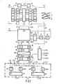
- the ternary signal to be regenerated - in the exemplary embodiment a pseudoternary AMI-coded signal A - is fed to two window comparators K1 and K2.
- the positive pulses of the signal A fall into the window of the comparator K1 and the negative into the window of the comparator K2.
- a binary one is present at the output of the comparator K1, while the output of the comparator K2 assumes the potential corresponding to a binary zero.
- a shift register SR1, SR2 is provided for each comparator, through which the binary samples are shifted with the clock f10 and transferred to a buffer S1, S2 in parallel with the clock f.
- the phase position of the symbol clock f, based on the signal A, can be any; therefore it is not necessary for the clock f to be recovered from the signal A. Any clock source with the nominal frequency of the symbol clock associated with signal A is sufficient.
- the clocks f10 and f have a time-independent phase relation to each other.
- SR1 which is just as large as the number of binary memory cells in the intermediate memories S1 and S2, is so large - namely 13 - that, regardless of the phase position of the clock f, 10 groups of four successive samples each -k is therefore too in the present example four have been elected - have space. In this way it is ensured that with each clock pulse of the clock f all samples of a signal element that fall into the eye of the signal A are in the buffer S1 or S2 as a seamless sequence. In addition, it is assumed that at least four samples of each signal element fall into the eye of signal A, the eye width as 6 is at least 2/5 of the nominal period of the symbol clock f.
- the purpose of the other circuit parts is, among other things, to automatically determine where the eye of the ternary signal A is located within the signal sections stored in the intermediate memories S1 and S2 and with each clock edge of the symbol clock f one of the sample values belonging to the eye from the intermediate memory S1 to the output AP or forward from the buffer S1 to the output AN.
- the binary ones in the buffer stores S1 and S2 are used to determine the position of the eye. If binary bars occur more frequently with the clock edges of the clock f on the same four successive memory cells of the buffer memories S1 or S2, these locations are regarded as the center of the eye of the signal A.
- the possible position of the center of the eye is determined by the logic L to which the buffer store S1 is connected via the connections E11 to E113 and the buffer store S2 via the connections E21 to E213.
- the exact structure of the logic L is shown in FIG. 2.
- the first four memory locations of the intermediate memory S1 are connected to the four inputs of an AND gate ULI via the connections E11 to E14.
- the memory cells 2 to 5 of the buffer S1 are connected via the connections E12 to E15 to the inputs of a further AND gate UL2 and so on to the memory locations 10 to 13, which have a tenth AND- via the connections E110 to E113 to the inputs.
- Gates UL10 are connected. The same applies to the connection of the memory locations of the buffer store S2 via the connections E21 to E213 to the AND gates UR1 to UR10.
- the outputs of the AND gates UL1 and UR1, which form a pair of gates, are connected to an OR gate OL1.
- a binary one occurs at the output of this OR gate OL1 if only binary ones are contained in the first four memory locations of the intermediate memory S1 or in the first four memory locations of the intermediate memory S2.
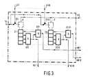
- the outputs of the OR gates OL1 to OL10 are at the same time the outputs of the logic L, they are connected via lines LS1 to LS10 to the inputs of a switching mechanism SW which is used to count how often binary at the outputs of the OR gates OL1 to OL10 Ones occur.
- FIG. 3 shows details of the switching mechanism SW - 10 counters Z1 to Z10 are provided, one of which is assigned to one of the OR gates OL1 to OL10 is. If a binary one occurs at the output of one of these OR gates at a clock instant of clock f, the assigned counter is incremented by one counter unit.
- switches SS1 to SS10 are provided, the control inputs of which are connected to one of the lines LS1 to LS10. A binary one on one of these lines closes the assigned switch, via which a clock pulse of the clock fs is then fed to the counter input of the connected counter.
- the clock fs is the symbol clock f which is phase-shifted by 90 °; the phase shift is necessary so that signal propagation times do not lead to malfunctions.
- the phase relation of all clocks used in the exemplary embodiment is shown schematically in the upper right part of FIG. 1.
- Each of the 4-stage counters Z1 to Z10 of the switching mechanism SW is provided with an interrogation circuit which consists of two AND gates.
- the first AND gate US1 to US10 is used to AND the three stages with the highest value of each counter Z1 to Z10.
- a binary one appears at the output of the AND gates US1 to US10 when the connected counter has reached a level of at least 14. These binary ones are led via lines AG1 to AG10 to the inputs of a third buffer S3 with ten storage locations.
- a binary one occurs at the output of the second AND gate UR1 to UR10 of each interrogation circuit as long as the connected counter is at its highest level, namely 15.
- the outputs of the second AND gates UR1 to UR10 are led via lines AW1 to AW10 to an OR gate 01 with ten inputs, at the output of which a binary one then occurs when at least one of the counters Z1 to Z10 has reached its maximum level.
- the output signal of the OR gate 01 is linked to the inverted symbol clock f by an AND gate U1, the output signal of which is used to clock the buffer store S3, into which the binary values on the lines AG1 to AG10 are adopted.
- a binary one in the memory locations of the intermediate store S3 indicates which of the counters Z1 to Z10 has reached status 14 or 15. Is this e.g. in the case of the counter Z10, this means that in the last four memory locations of the intermediate memory S1 or in the last four memory locations of the intermediate memory S2 there were only binary ones at 14 or 15 clock pulses of the symbol clock f.
- the signal sections which are buffered in the last four memory locations of the buffer memories S1 and S2 belong to the center of the eye of the signal A and the sample value stored in the memory location 13 of the buffer memory S1 becomes the output AP and the one stored in memory location 13 of the buffer memory S2 Sample placed at the output AN of the circuit of FIG. 1.
- the buffer S3 is followed by a selection circuit AWS, the inputs of which are connected via terminals BK1 to BK10 to the outputs of stages 1 to 10 of the buffer S3.
- An output is assigned to each input of the selection circuit AWS. If a binary one is present at several inputs of the selection circuit AWS, this is only forwarded to the assigned output at one input, while a binary zero is present at all other outputs.
- the binary values at the outputs of the selection circuit are led via lines AS1 to AS10 to the memory locations 1 to 10 of a fourth clocked buffer store S4, the function of which is explained in more detail below.
- a memory location other than the tenth memory location of the buffer memory S4 contains the binary one, then another of the AND gates UP1 to UP10 or UN1 to UN10 of the gate circuit GS is opened, and the stored binary values of other memory locations of the buffer memories S1 and S2 become passed to the outputs AP and AN for further processing.
- the search is repeated by deleting all counters as soon as a counter has reached its maximum level.
- the erase pulse for the counter is obtained from the output signal of the AND gate U1 and a clock Ts - which is phase-shifted by 270 ° with respect to the symbol clock f. Both signals become one em supplied another AND gate U2, the output of which is connected via a line RS to the reset inputs R of all counters Z1 to Z10.
- the content of the buffer S4 defines the storage locations of the buffer memories S1 and S2, the binary values of which are forwarded to the outputs AP and AN; it therefore determines the sampling phase of signal A.
- the eye of the signal A enlarged over time, the sampling phase position selected before the eye enlargement is just as suitable as e.g. a new phase sample position that would result solely from the functioning of the selection circuit AWS.
- a comparator VG with 20 inputs is provided, which are connected to terminals AK1 to AK10 and BK1 to BK10.
- the comparator VG only outputs a clock pulse to the buffer S4 if the sampling phase before changing the eye is not included in the permissible sampling phase after changing the eye, ie if none of the AND operations between the two signals at terminals AK1 and BK1 to AK10 and BK10 assume the value one. Only in this case are the binary values present at the output of the selection circuit AWS in the buffer S4 with the clock pulse of the comparator VG, the memory location in which the only binary one is stored determining the new sampling phase position.
Abstract
Description
Die Erfindung betrifft eine Schaltungsanordnung zur Abtastung eines ternären Signales, bei der das ternäre Signal an die Eingänge zweier Fensterkomparatoren geführt ist und seine größten Amplituden in das Fenster des ersten und seine kleinsten Amplituden in das Fenster des zweiten Fensterkomparators fallen.The invention relates to a circuit arrangement for sampling a ternary signal, in which the ternary signal is fed to the inputs of two window comparators and its greatest amplitudes fall in the window of the first and its smallest amplitudes in the window of the second window comparator.
Eine Schaltungsanordnung dieser Art kann z.B. in Regeneratoren verwendet werden, mit denen AMI-codierte Leitungssignale regeneriert werden sollen.A circuit arrangement of this type can e.g. are used in regenerators with which AMI-coded line signals are to be regenerated.
Aus der DE-C2-2 827 958 ist ein Regenerator bekannt, bei dem zur Regeneration eines n-ären Signals mit n Amplitudenstufen, n-1 Amplitudenentscheider (Fensterkomparatoren) verwendet werden, deren überlagerte Ausgangssignale das regenerierte n-äre Signal ergeben.From DE-C2-2 827 958 a regenerator is known in which n-1 amplitude deciders (window comparators) are used for the regeneration of an n-ary signal with n amplitude stages, the superimposed output signals of which result in the regenerated n-ary signal.
Bevor das n-äre Signal den Amplitudenentscheidern zugeführt wird, durchläuft es eine mit dem Symboltakt des n-ären Signales getaktete Abtaststufe, mit der zu den gewünschten Abtastzeitpunkten -nämlich in Augenmitte -Signalteile ausgeblendet werden.Before the n-ary signal is fed to the amplitude decision-makers, it passes through a sampling stage clocked with the symbol clock of the n-ary signal, with which signal portions are masked out at the desired sampling times, namely in the middle of the eye.
In der zitierten Literaturstelle ist jedoch nicht angegeben, wie die Phasenlage des Symboltaktes zu beeinflussen ist, damit die Abtastung tatsächlich etwa in Augenmitte -also optimal -erfolgt. Besondere Schwierigkeiten treten dann auf, wenn sich die Augenöffnung eines zu regenerierenden Nutzsignales im Laufe der Übertragung ändern kann, so daß eine optimale Abtastung zu Zeitpunkten erfolgen muß, die von vornherein nicht festlegbar sind. Eine solche Veränderung der Augenöffnung tritt z.B. an der Schnittstelle S (CCITT-Empfehlung 1.430 Section 3) des zukünftigen dienstintegrierten digitalen Fernmeidenetzes ISDN auf. Beim Nutzsignal handelt es sich in diesem Falle um ein Multiplexsignal, das aus den Signalen der Teilnehmerendeinrichtungen zusammengesetzt wird, deren Aktivitäten von einem Netzabschlußgerät synchronisiert werden. Beginnt eine Teilnehmerendeinrichtung zu senden, während eine andere schon ihr Sendesignal abgibt, so tritt im Gesamtsignal eine Verkleinerung der Augenöffnung ein, deren Größe von der unterschiedlichen Signallaufzeit zwischen Teilnehmerendeinrichtung und Netzabschlußgerät abhängt.However, the cited reference does not specify how the phase position of the symbol clock is to be influenced, so that the scanning actually takes place approximately in the middle of the eye - so optimally. Particular difficulties arise when the eye opening of a useful signal to be regenerated can change in the course of the transmission, so that an optimal scanning must take place at times that cannot be determined from the outset. Such a change in the eye opening occurs e.g. at interface S (CCITT recommendation 1.430 Section 3) of the future integrated digital long-distance network ISDN. In this case, the useful signal is a multiplex signal which is composed of the signals from the subscriber terminals whose activities are synchronized by a network termination device. If a subscriber terminal begins to transmit while another is already emitting its transmission signal, the overall signal is reduced in size, the size of the eye opening depending on the different signal delay between the subscriber terminal and the network termination device.
Der Erfindung liegt 'die Aufgabe zu grunde, eine Abtastschaltung der eingangs genannten Art anzugeben, durch die die optimale Abtastphasenlage laufend aus dem ternären Nutzsignal ermittelt wird.The invention is based 'on the object to provide a sampling of the type mentioned by which the optimal sampling phase is determined continuously from the ternary payload.
Diese Aufgabe wird bei einer Schaltungsanordnung der eingangs genannten Art dadurch gelöst,
- daß das Ausgangssignal eines jeden Fensterkomparators mit einem zum Symboltakt des ternären Signales phasenstarren Takt der m-fachen Symboltaktfrequenz abgetastet wird,
- daß die binären Abtastwerte durch jeweils ein Schieberegister mit mindestens m Stufen geschoben werden und der Inhalt der Schieberegister mit dem Symboltakt in jeweils einen Zwischenspeicher übernommen wird,
- daß die Ausgänge der beiden Zwischenspeicher mit den Eingängen einer Logik verbunden sind und jeder Gruppe von k aufeinander folgender Speicherstellen des ersten Zwischenspeichers und der entsprechenden Gruppe des zweiten Zwischenspeichers ein Ausgang der Logik zugeordnet ist,
- daß an diesem Ausgang eine binäre Eins anliegt. wenn eine der beiden Gruppen von Speicherstellen nur binären Einsen enthalten,
- daß mit jeder binären Eins an einem Ausgang der Logik ein diesem Ausgang zugeordneter Zähler inkrementiert wird,
- daß das Errreichen eines ersten vorbestimmten Standes eines jeden Zählers dann als binäre Eins in die Speicherstellen eines dritten Zwischenspeichers übernommen wird, wenn einer der Zähler einen zweiten, jedoch höheren vorbestimm- . ten Stand erreicht hat, und daß alle Zähler zurückgesetzt werden
- daß alle Speicherstellen des dritten Zwischenspeichers mit den Eingängen einer Auswahlschaltung verbunden sind, die nur eine die an ihre Eingängen anliegenden Einsen an den zugeordneten Ausgang weitergibt,
- daß mit den Signalen am Ausgang der Auswahlschaltung eine Gatter-Schaltung für einen der im ersten und einen der im zweiten Zwischenspeicher gespeicherten binären Abtastwerte durchlässig geschaltet wird.
- that the output signal of each window comparator is sampled with a clock of m times the symbol clock frequency which is phase-locked to the symbol clock of the ternary signal,
- that the binary samples are shifted through a shift register each with at least m levels and the content of the shift register is transferred to a buffer with the symbol clock,
- that the outputs of the two buffers are connected to the inputs of a logic and that an output of the logic is assigned to each group of k successive memory locations of the first buffer and the corresponding group of the second buffer,
- that a binary one is present at this output. if one of the two groups of storage locations contains only binary ones,
- that with each binary one at an output of the logic, a counter assigned to this output is incremented,
- that the reaching of a first predetermined level of each counter is then adopted as a binary one in the memory locations of a third buffer when one of the counters predetermines a second, but higher. has reached ten level and that all counters are reset
- that all memory locations of the third buffer are connected to the inputs of a selection circuit which only one passes on the ones present at its inputs to the assigned output,
- that with the signals at the output of the selection circuit, a gate circuit for one of the binary samples stored in the first and in the second buffer is switched to be transparent.
Die erfindungsgemäße Anordnung zeichnet sich dadurch aus, daß sie nur aus digitalen Bausteinen besteht und daher ohne weiteres als integrierter Schaltkreis ausführbar ist.The arrangement according to the invention is characterized in that it consists only of digital components and can therefore be easily implemented as an integrated circuit.
Vorteilhafte Ausgestaltungen und Weiterbildungen der Erfindung sind den Unteransprüchen zu entnehmen.Advantageous refinements and developments of the invention can be found in the subclaims.
Anhand der Figuren soll ein Ausführungsbeispiel der Erfindung näher erläutert werden.
- Fig. 1 zeigt das Blockschaltbild eines Ausführungsbeispieles der Erfindung.
- Fig. 2 und Fig. 3 zeigen den inneren Aufbau von Funk tionsblöcken der Fig. 1.
- Fig. 1 shows the block diagram of an embodiment of the invention.
- FIG. 2 and FIG. 3 show the internal structure of the function blocks of FIG. 1.
Nach Fig. 1 wird das zu regenerierende ternäre Signal -im Ausführungsbeispiel ein pseudoternäres AMI-kodiertes Signal A -zwei Fensterkomparatoren K1 und K2 zugeführt. Die positiven Impulse des Signales A fallen in das Fenster des Komparators K1 und die negativen in das Fenster des Komparators K2. Bei einem positiven Impuls liegt also am Ausgang des Komparators K1 eine binäre Eins an, während der Ausgang des Komparators K2 das einer binären Null entsprechende Potential annimmt.1, the ternary signal to be regenerated - in the exemplary embodiment a pseudoternary AMI-coded signal A - is fed to two window comparators K1 and K2. The positive pulses of the signal A fall into the window of the comparator K1 and the negative into the window of the comparator K2. In the event of a positive pulse, a binary one is present at the output of the comparator K1, while the output of the comparator K2 assumes the potential corresponding to a binary zero.
Denkbar sind auch Ausführungsformen, bei denen diese und in der folgenden Beschreibung erwähnten Binärwerte durch ihre Komplemente ersetzt sind. Die gewählte Festlegung der Binärwerte ist jedoch für die Erfindung unwesentlich und dient nur ihrer einfacheren Verdeutlichung.Embodiments are also conceivable in which these binary values and those mentioned in the following description are replaced by their complements. The chosen definition of the binary values is, however, insignificant for the invention and only serves to simplify it.
Die Binärwerte an den Ausgängen der Komparatoren K1 und K2 werden mit einem Takt f10 abgetastet, dessen Taktfrequenz das Zehnfache des zum Signal A gehörigen Symboltaktes f beträgt; im vorliegenden Beispiel ist also m = 10 gewählt. Für jeden Komparator ist ein Schieberegister SR1, SR2 vorgeshen, durch das die binären Abtastwerte mit dem Takt f10 geschoben und parallel mit dem Takt f in einen Zwischenspeicher S1, S2 übernommen werden. Die Phasenlage des Symboltaktes f, bezogen auf das Signal A, kann beliebig sein; deshalb ist es auch nicht erforderlich, daß der Takt f aus dem Signal A zurückgewonnen wird. Es reicht eine beliebige Taktquelle mit der nominellen Frequenz des zum Signal A-gehörigen Symboltaktes. Die Takte f10 und f haben allerdings eine zeitunabhängiger Phasenrelation zueinander.The binary values at the outputs of the comparators K1 and K2 are sampled with a clock f10, the clock frequency of which is ten times the symbol clock f associated with the signal A; in the present example, m = 10 is selected. A shift register SR1, SR2 is provided for each comparator, through which the binary samples are shifted with the clock f10 and transferred to a buffer S1, S2 in parallel with the clock f. The phase position of the symbol clock f, based on the signal A, can be any; therefore it is not necessary for the clock f to be recovered from the signal A. Any clock source with the nominal frequency of the symbol clock associated with signal A is sufficient. The clocks f10 and f have a time-independent phase relation to each other.
Die Anzahl der Stufen der Schieberegister SR1. SR2, die ebenso groß ist wie die Anzahl der binären Speicherzellen der Zwischenspeicher S1 und S2, ist so groß -nämlich 13 -gewählt, daß unabhängig von der Phasenlage des Taktes f 10 Gruppen zu je vier aufeinanderfolgende Abtastwerte -k ist also im vorliegenden Beispiel zu vier gewählt worden -darin Platz haben. Auf diese Weise wird sichergestellt, daß mit jedem Taktimpuls des Taktes f alle Abtastwerte eines Signalelementes, die in das Auge des Signales A fallen, als lückenlose Folge im Zwischenspeicher S1 oder S2 stehen. Außerdem ist unterstellt, daß mindestens vier Abtastwerte eines jeden Signalelementes in das Auge des Signales A fallen, die Augenbreite als6 mindestens 2/5 der nominellen Periodendauer des Symboltaktes f beträgt.The number of stages of the shift register SR1. SR2, which is just as large as the number of binary memory cells in the intermediate memories S1 and S2, is so large - namely 13 - that, regardless of the phase position of the clock f, 10 groups of four successive samples each -k is therefore too in the present example four have been elected - have space. In this way it is ensured that with each clock pulse of the clock f all samples of a signal element that fall into the eye of the signal A are in the buffer S1 or S2 as a seamless sequence. In addition, it is assumed that at least four samples of each signal element fall into the eye of signal A, the eye width as 6 is at least 2/5 of the nominal period of the symbol clock f.
Zweck der weiteren Schaltungsteile ist nun unter anderem, automatisch festzustellen, wo sich innerhaib der in den Zwischenspeichern S1 und S2 gespeicherten Signalabschnitten das Auge des ternären Signales A befindet und mit jeder Taktflanke des Symboltaktes f einen der zum Auge gehörigen Abtastwerte vom Zwischenspeicher S1 zum Ausgang AP bzw. vom Zwischenspeicher S1 zum Ausgang AN weiterzuleiten.The purpose of the other circuit parts is, among other things, to automatically determine where the eye of the ternary signal A is located within the signal sections stored in the intermediate memories S1 and S2 and with each clock edge of the symbol clock f one of the sample values belonging to the eye from the intermediate memory S1 to the output AP or forward from the buffer S1 to the output AN.
Zur Feststellung der Lage des Auges werden die binären Einsen in den Zwischenspeichern S1 und S2 verwendet. Treten häufiger mit den Taktflanken des Taktes f an den gleichen vier aufeinanderfolgenden Speicherzellen der Zwischenspeicher S1 oder S2 binäre Eisen auf, so werden diese Stellen als die Augenmitte des Signales A angesehen. Mögliche Lage der Augenmitte ermittelt die Logik L, mit der der Zwischenspeicher S1 über die Anschlüsse E11 bis E113 bzw. der Zwischenspeicher S2 über die Anschlüsse E21 bis E213 verbunden ist.The binary ones in the buffer stores S1 and S2 are used to determine the position of the eye. If binary bars occur more frequently with the clock edges of the clock f on the same four successive memory cells of the buffer memories S1 or S2, these locations are regarded as the center of the eye of the signal A. The possible position of the center of the eye is determined by the logic L to which the buffer store S1 is connected via the connections E11 to E113 and the buffer store S2 via the connections E21 to E213.
Der genaue Aufbau der Logik L ist in Fig. 2 gezeigt. Über die Anschlüsse E11 bis E14 sind die ersten vier Speicherstellen des Zwischenspeichers S1 mit den vier Eingängen eines UND-Gatters ULI verbunden. Die Speicherzellen 2 bis 5 des Zwischenspeichers S1 sind über die Anschlüsse E12 bis E15 mit den Eingängen eines weiteren UND-Gatters UL2 verbunden und so fort bis zu den Speicherstellen 10 bis 13, die über die Anschlüsse E110 bis E113 mit den Eingängen einen zehnten UND-Gatters UL10 verbunden sind. Entsprechendes gilt für die Verbindung der Speicherstellen des Zwischenspeichers S2 über die Anschlüsse E21 bis E213 mit den UND-Gattern UR1 bis UR10.The exact structure of the logic L is shown in FIG. 2. The first four memory locations of the intermediate memory S1 are connected to the four inputs of an AND gate ULI via the connections E11 to E14. The
Die Ausgänge der UND-Gatter UL1 und UR1, die ein Gatterpaar bilden, sind an ein ODER-Gatter OL1 geführt. Am Ausgang dieses ODER-Gatters OL1 tritt eine binäre Eins auf, wenn in den ersten vier Speicherstellen des Zwischenspeichers S1 oder in den ersten vier Speicherstellen des Zwischenspeichers S2 nur binäre Einsen enthalten sind. Wiederum gilt entsprechendes für die UND-Gatterpaare UL2 und UR2 bis UL10 und UR10 und die ODER-Gatter OL2 bis OL10. Die Ausgänge der ODER-Gatter OL1 bis OL10 sind gleichzeitig die Ausgänge der Logik L, sie sind über Leitungen LS1 bis LS10 mit den Eingängen eines Schaltwerkes SW verbunden, mit dem gezählt wird, wie oft an den Ausgängen der ODER-Gatter OL1 bis OL10 binäre Einsen auftreten. Für diesen Zweck -Fig. 3 zeigt Einzelheiten des Schaltwerkes SW -sind 10 Zähler Z1 bis Z10 vorgesehen, von denen je einer einem der ODER-Gatter OL1 bis OL10 zugeordnet ist. Tritt am Ausgang eines dieser ODER-Gatter zu einem Taktzeitpunkt des Taktes f eine binäre Eins auf, so wird der zugeordnete Zähler um eine Zählereinheit inkrementiert. Zur Inkrementierung der Zähler Z1 bis Z10 sind Schalter SS1 bis SS10 vorgesehen, deren Steuereingänge mit je einer der Leitungen LS1 bis LS10 verbunden sind. Eine binäre Eins auf eine dieser Leitungen schließt den zugeordneten Schalter, über den dann ein Taktimpuls des Taktes fs dem Zähleingang des angeschlossenen Zählers zugeführt wird. Der Takt fs ist der um 90° phasenverschobene Symboltakt f; die Phasenverschiebung ist notwendig, damit signallaufzeiten nicht zu Fehlfunktionen führen. Die Phasenrelation aller beim Ausführungsbeispiel verwendeten Takte ist im oberen rechten Teil der Fig. 1 - schematisch dargestellt.The outputs of the AND gates UL1 and UR1, which form a pair of gates, are connected to an OR gate OL1. A binary one occurs at the output of this OR gate OL1 if only binary ones are contained in the first four memory locations of the intermediate memory S1 or in the first four memory locations of the intermediate memory S2. The same applies in turn to the AND gate pairs UL2 and UR2 to UL10 and UR10 and the OR gates OL2 to OL10. The outputs of the OR gates OL1 to OL10 are at the same time the outputs of the logic L, they are connected via lines LS1 to LS10 to the inputs of a switching mechanism SW which is used to count how often binary at the outputs of the OR gates OL1 to OL10 Ones occur. For this purpose -Fig. 3 shows details of the switching mechanism SW - 10 counters Z1 to Z10 are provided, one of which is assigned to one of the OR gates OL1 to OL10 is. If a binary one occurs at the output of one of these OR gates at a clock instant of clock f, the assigned counter is incremented by one counter unit. To increment the counters Z1 to Z10, switches SS1 to SS10 are provided, the control inputs of which are connected to one of the lines LS1 to LS10. A binary one on one of these lines closes the assigned switch, via which a clock pulse of the clock fs is then fed to the counter input of the connected counter. The clock fs is the symbol clock f which is phase-shifted by 90 °; the phase shift is necessary so that signal propagation times do not lead to malfunctions. The phase relation of all clocks used in the exemplary embodiment is shown schematically in the upper right part of FIG. 1.
Jeder der 4-stufigen Zähler Z1 bis Z10 des Schaltwerkes SW ist mit einer Abfrageschaltung versehen, die aus zwei UND-Gattern besteht. Mit dem ersten UND-Gatter US1 bis US10 wird eine UND-Verknüpfung der drei Stufen mit höchster Wertigkeit eines jeden Zählers Z1 bis Z10 vorgenommen. Am Ausgang der UND-Gatter US1 bis US10 erscheint eine binäre Eins, wenn der angeschlossene Zähler einen Stand von mindestens 14 erreicht hat. Diese binären Einsen werden über Leitungen AG1 bis AG10 an die Eingänge eines dritten Zwischenspeichers S3 mit zehn Speicherstellen geführt.Each of the 4-stage counters Z1 to Z10 of the switching mechanism SW is provided with an interrogation circuit which consists of two AND gates. The first AND gate US1 to US10 is used to AND the three stages with the highest value of each counter Z1 to Z10. A binary one appears at the output of the AND gates US1 to US10 when the connected counter has reached a level of at least 14. These binary ones are led via lines AG1 to AG10 to the inputs of a third buffer S3 with ten storage locations.
Am Ausgang des zweiten UND-Gatters UR1 bis UR10 einer jeden Abfrageschaltung tritt eine binäre Eins auf solange der angeschlossene Zähler auf seinem Höchststand, nämlich 15 steht.A binary one occurs at the output of the second AND gate UR1 to UR10 of each interrogation circuit as long as the connected counter is at its highest level, namely 15.
Die Ausgänge der zweiten UND-Gatter UR1 bis UR10 sind über Leitungen AW1 bis AW10 an ein ODER-Gatter 01 mit zehn Eingängen geführt, an dessen Ausgang folglich dann eine binäre Eins auftritt, wenn mindestens einer der Zähler Z1 bis Z10 seinen Höchststand erreicht hat.The outputs of the second AND gates UR1 to UR10 are led via lines AW1 to AW10 to an
Zur Formung von Taktimpulsen wird das Ausgangssignal der ODER-Gatter 01 mit dem invertierten Symboltakt f durch ein UND-Gatter U1 verknüpft, mit dessen Ausgangssignal der Zwischenspeicher S3 getaktet wird, in den die Binärwerte auf den Leitungen AG1 bis AG10 übernommen werden. Nach dem Auftreten eines Taktimpulses auf einer Leitung TS zeigt eine binäre Eins in den Speicherstellen des Zwischenspeichers S3 an, welcher der Zähler Z1 bis Z10 den Stand 14 oder 15 erreicht hat. Ist dies z.B. beim Zähler Z10 der Fall, so heißt das, daß in den letzten vier Speicherstellen des Zwischenspeichers S1 oder in den letzten vier Speicherstellen des Zwischenspeichers S2 bei 14 oder 15 Taktimpulsen des Symboltaktes f nur binäre Einsen gestanden haben. Folglich gehören die Signalausschnitte, die in den letzten vier Speicherstellen der Zwischenspeicher S1 und S2 zwischengespeichert werden, zur Augenmitte des Signales A und es wird der in der Speicherstelle 13 des Zwischenspeichers S1 gespeicherte Abtastwert an den Ausgang AP und der in Speicherstelle 13 des Zwischenspeichers S2 gespeicherte Abtastwert an den Ausgang AN der Schaltung nach Fig. 1 gelegt.To form clock pulses, the output signal of the
Zur Durchführung dieses Vorganges folgt auf den Zwischenspeicher S3 eine Auswahlschaltung AWS, deren Eingänge über Klemmen BK1 bis BK10 mit den Ausgängen der Stufe 1 bis 10 des Zwischenspeichers S3 verbunden sind. Jedem Eingang der Auswahlschaltung AWS ist ein Ausgang zugeordnet. Liegt an mehreren Eingängen der Auswahlschaltung AWS eine binäre Eins an, so wird diese nur bei einem Eingang an den zugeordneten Ausgang weitergeleitet, während an allen anderen Ausgängen eine binäre Null anliegt. Die Binärwerte an den Ausgängen der Auswahlschaltung werden über Leitungen AS1 bis AS10 an die Speicherstellen 1 bis 10 einer vierten getakteten Zwischenspeichers S4 geführt, dessen Funktion weiter unten genauer erläutert wird.To carry out this process, the buffer S3 is followed by a selection circuit AWS, the inputs of which are connected via terminals BK1 to BK10 to the outputs of
Ist nun z.B. in der zehnten Speicherstelle des Zwischenspeichers S4 eine binäre Eins gespeichert -alle anderen Speicherstellen enthalten dann binären Nullen -so werden die UND-Gatter UP10 und UN10 einer an den Zwischenspeicher S4 angeschlossenen Gatterschaltung GS geöffnet. Im Falle des Gatters UP10, dessen zweiter Eingang mit der Klemme E113 verbunden ist. gelangt die in der dreizehnten Speicherstelle des Zwischenspeichers S1 gespeicherte Information an den Gatterausgang und über ein ODER-Gatter OP an den Ausgang AP. Im Falle des, Gatters UN10, dessen zweiter Eingang mit der Klemme E213 verbunden ist, gelangt die in der dreizehnten Speicherstelle des Zwischenspeichers S2 gespeicherte Information an den Gatterausgang und über ein ODER-Gatter ON an den Ausgang AN.Is now e.g. A binary one is stored in the tenth memory location of the intermediate memory S4 - all other memory locations then contain binary zeros - this is how the AND gates UP10 and UN10 of a gate circuit GS connected to the intermediate memory S4 are opened. In the case of gate UP10, the second input of which is connected to terminal E113. the information stored in the thirteenth memory location of the buffer S1 reaches the gate output and, via an OR gate OP, the output AP. In the case of the gate UN10, the second input of which is connected to the terminal E213, the information stored in the thirteenth memory location of the buffer store S2 reaches the gate output and, via an OR gate ON, the output AN.
Enthält eine andere als die zehnte Speicherstelle des Zwischenspeichers S4 die binäre Eins, so wird auch ein anderes der UND-Gatter UP1 bis UP10, bzw. UN1 bis UN10 der Gatterschaltung GS geöffnet, und es werden die gespeicherten Binärwerte anderer Speicherstellen der Zwischenspeicher S1 und S2 an die Ausgänge AP und AN zur weiteren Verarbeitung geleitet.If a memory location other than the tenth memory location of the buffer memory S4 contains the binary one, then another of the AND gates UP1 to UP10 or UN1 to UN10 of the gate circuit GS is opened, and the stored binary values of other memory locations of the buffer memories S1 and S2 become passed to the outputs AP and AN for further processing.
Ist mit Hilfe des Schaltwerkes SW und dessen Zähler Z1 bis Z10 die Lage des Auges gefunden worden, so wird die Suche wiederholt, indem alle Zähler gelöscht werden, sobald ein Zähler seinen Höchststand erreicht hat. Der Löschimpuls für die Zähler wird aus dem Ausgangssignal des UND-Gatters U1 und einem Takt Ts- gewonnen, der gegenüber dem Symboltakt f um 270° phasenverschoben ist. Beide Signale werden einem weiteren UND-Gatter U2 zugeführt, dessen Ausgang über eine Leitung RS mit den Rücksätzeingängen R sämtlicher Zähler Z1 bis Z10 verbunden ist.If the position of the eye has been found with the aid of the switching mechanism SW and its counters Z1 to Z10, the search is repeated by deleting all counters as soon as a counter has reached its maximum level. The erase pulse for the counter is obtained from the output signal of the AND gate U1 and a clock Ts - which is phase-shifted by 270 ° with respect to the symbol clock f. Both signals become one em supplied another AND gate U2, the output of which is connected via a line RS to the reset inputs R of all counters Z1 to Z10.
Wie oben schon angedeutet, legt der Inhalt des Zwischenspeichers S4 die Speicherstellen der Zwischenspeicher S1 und S2 fest, deren Binärwerte an die Ausgänge AP und AN weitergeleitet werden; er bestimmt also die Abtastphasenlage des Signales A. Wird z.B. das Auge des Signales A im Laufe der Zeit vergrößert, so ist die vor der Augenvergrößerung gewählte Abtastphasenlage ebenso geeignet wie z.B. eine neue Phasenabtastlage, die sich allein aufgrund der Funktionsweise der Auswahlschaltung AWS ergeben würde. Um unnötige Sprünge in der Abtastphasenlage zu vermeiden, ist ein Vergleicher VG mit 20 Eingängen vorgesehen, die mit den Klemmen AK1 bis AK10 und BK1 bis BK10 verbunden sind. Der Vergleicher VG gibt nur dann einen Taktimpuls an den Zwischenspeicher S4 ab, wenn die Abtastphasenlage vor einer Änderung des Auges nicht in den zulässigen Abtastphasenlagen nach Änderung des Auges enthalten ist, d.h., wenn keine der UND-Verknüpfungen zwischen den beiden Signalen an den Klemmen AK1 und BK1 bis AK10 und BK10 den Wert Eins annimmt. Nur in diesem Fall werden mit dem Taktimpuls des Vergleichers VG die am Ausgang der Auswahlschaltung AWS anliegenden Binärwerte in den Zwischenspeicher S4 übernommen, wobei die Speicherstelle, in der die einzige binäre Eins gespeichert ist, die neue Abtastphasenlage festlegt.As already indicated above, the content of the buffer S4 defines the storage locations of the buffer memories S1 and S2, the binary values of which are forwarded to the outputs AP and AN; it therefore determines the sampling phase of signal A. the eye of the signal A enlarged over time, the sampling phase position selected before the eye enlargement is just as suitable as e.g. a new phase sample position that would result solely from the functioning of the selection circuit AWS. To avoid unnecessary jumps in the sampling phase, a comparator VG with 20 inputs is provided, which are connected to terminals AK1 to AK10 and BK1 to BK10. The comparator VG only outputs a clock pulse to the buffer S4 if the sampling phase before changing the eye is not included in the permissible sampling phase after changing the eye, ie if none of the AND operations between the two signals at terminals AK1 and BK1 to AK10 and BK10 assume the value one. Only in this case are the binary values present at the output of the selection circuit AWS in the buffer S4 with the clock pulse of the comparator VG, the memory location in which the only binary one is stored determining the new sampling phase position.
Claims (9)
Priority Applications (1)
| Application Number | Priority Date | Filing Date | Title |
|---|---|---|---|
| AT86200957T ATE81571T1 (en) | 1985-06-04 | 1986-06-02 | CIRCUIT ARRANGEMENT FOR SENSING A TERNAL SIGNAL. |
Applications Claiming Priority (2)
| Application Number | Priority Date | Filing Date | Title |
|---|---|---|---|
| DE19853519929 DE3519929A1 (en) | 1985-06-04 | 1985-06-04 | CIRCUIT ARRANGEMENT FOR SCANING A TERNAERAL SIGNAL |
| DE3519929 | 1985-06-04 |
Publications (3)
| Publication Number | Publication Date |
|---|---|
| EP0204376A2 true EP0204376A2 (en) | 1986-12-10 |
| EP0204376A3 EP0204376A3 (en) | 1989-01-04 |
| EP0204376B1 EP0204376B1 (en) | 1992-10-14 |
Family
ID=6272359
Family Applications (1)
| Application Number | Title | Priority Date | Filing Date |
|---|---|---|---|
| EP86200957A Expired - Lifetime EP0204376B1 (en) | 1985-06-04 | 1986-06-02 | Ternary signal scanning device |
Country Status (6)
| Country | Link |
|---|---|
| US (1) | US4700359A (en) |
| EP (1) | EP0204376B1 (en) |
| JP (1) | JPS61280146A (en) |
| AT (1) | ATE81571T1 (en) |
| CA (1) | CA1271531A (en) |
| DE (2) | DE3519929A1 (en) |
Cited By (1)
| Publication number | Priority date | Publication date | Assignee | Title |
|---|---|---|---|---|
| EP0556697A1 (en) * | 1992-02-19 | 1993-08-25 | Siemens Aktiengesellschaft | Method and device for the transmission of additional information |
Families Citing this family (7)
| Publication number | Priority date | Publication date | Assignee | Title |
|---|---|---|---|---|
| USRE34206E (en) * | 1988-10-24 | 1993-03-30 | Northern Telecom Limited | Method and apparatus for timing recovery |
| US4896334A (en) * | 1988-10-24 | 1990-01-23 | Northern Telecom Limited | Method and apparatus for timing recovery |
| US5157690A (en) * | 1990-10-30 | 1992-10-20 | Level One Communications, Inc. | Adaptive convergent decision feedback equalizer |
| DE4303962A1 (en) * | 1993-02-10 | 1994-08-18 | Georg Dipl Ing Figol | Data regenerator |
| US6249557B1 (en) | 1997-03-04 | 2001-06-19 | Level One Communications, Inc. | Apparatus and method for performing timing recovery |
| US6167082A (en) * | 1997-03-06 | 2000-12-26 | Level One Communications, Inc. | Adaptive equalizers and methods for carrying out equalization with a precoded transmitter |
| DE19857396C2 (en) * | 1998-12-12 | 2002-11-14 | Josef Von Stackelberg | Fail-safe binary comparator with ternary result and status display |
Citations (5)
| Publication number | Priority date | Publication date | Assignee | Title |
|---|---|---|---|---|
| US3764989A (en) * | 1972-12-20 | 1973-10-09 | Ultronic Systems Inc | Data sampling apparatus |
| US3864529A (en) * | 1972-09-14 | 1975-02-04 | Lynch Communication Systems | Receiver for decoding duobinary signals |
| US4080572A (en) * | 1976-11-24 | 1978-03-21 | Westinghouse Electric Corporation | Receiver and method for synchronizing and detecting coded waveforms |
| DE2827958B1 (en) * | 1978-06-26 | 1979-09-27 | Siemens Ag | Section regenerator for multi-level digital signals in a partial response code |
| US4242755A (en) * | 1977-01-14 | 1980-12-30 | Thomson-Csf | Circuit arrangement for decoding digital signals |
Family Cites Families (1)
| Publication number | Priority date | Publication date | Assignee | Title |
|---|---|---|---|---|
| US4339823A (en) * | 1980-08-15 | 1982-07-13 | Motorola, Inc. | Phase corrected clock signal recovery circuit |
-
1985
- 1985-06-04 DE DE19853519929 patent/DE3519929A1/en not_active Withdrawn
-
1986
- 1986-05-30 JP JP61123839A patent/JPS61280146A/en active Pending
- 1986-06-02 AT AT86200957T patent/ATE81571T1/en not_active IP Right Cessation
- 1986-06-02 DE DE8686200957T patent/DE3686959D1/en not_active Expired - Lifetime
- 1986-06-02 EP EP86200957A patent/EP0204376B1/en not_active Expired - Lifetime
- 1986-06-03 US US06/870,272 patent/US4700359A/en not_active Expired - Lifetime
- 1986-06-04 CA CA000510856A patent/CA1271531A/en not_active Expired
Patent Citations (5)
| Publication number | Priority date | Publication date | Assignee | Title |
|---|---|---|---|---|
| US3864529A (en) * | 1972-09-14 | 1975-02-04 | Lynch Communication Systems | Receiver for decoding duobinary signals |
| US3764989A (en) * | 1972-12-20 | 1973-10-09 | Ultronic Systems Inc | Data sampling apparatus |
| US4080572A (en) * | 1976-11-24 | 1978-03-21 | Westinghouse Electric Corporation | Receiver and method for synchronizing and detecting coded waveforms |
| US4242755A (en) * | 1977-01-14 | 1980-12-30 | Thomson-Csf | Circuit arrangement for decoding digital signals |
| DE2827958B1 (en) * | 1978-06-26 | 1979-09-27 | Siemens Ag | Section regenerator for multi-level digital signals in a partial response code |
Non-Patent Citations (1)
| Title |
|---|
| ELECTRONICS, Band 6, Nr. 5, 1. M{rz 1973, Seiten 94-96, New York, US; T.R. BLAKESLEE: "Transformer-coupled transceiver speeds two-way data transmission" * |
Cited By (1)
| Publication number | Priority date | Publication date | Assignee | Title |
|---|---|---|---|---|
| EP0556697A1 (en) * | 1992-02-19 | 1993-08-25 | Siemens Aktiengesellschaft | Method and device for the transmission of additional information |
Also Published As
| Publication number | Publication date |
|---|---|
| ATE81571T1 (en) | 1992-10-15 |
| EP0204376A3 (en) | 1989-01-04 |
| CA1271531A (en) | 1990-07-10 |
| EP0204376B1 (en) | 1992-10-14 |
| JPS61280146A (en) | 1986-12-10 |
| DE3519929A1 (en) | 1986-12-04 |
| US4700359A (en) | 1987-10-13 |
| DE3686959D1 (en) | 1992-11-19 |
Similar Documents
| Publication | Publication Date | Title |
|---|---|---|
| DE2047001B2 (en) | Arrangements for the transmission of data within a data processing system | |
| DE2543130B2 (en) | Circuit arrangement for the transmission of digital data in VoUduplex operation between at least two stations | |
| DE1079100B (en) | Message transmission system, in particular for telegraphy switching | |
| DE1537248A1 (en) | Keyed direct current controlled bistable multivibrator with preferred position with simultaneous control | |
| DE2515801A1 (en) | PROCEDURES AND CIRCUIT ARRANGEMENTS FOR TIME MULTIPLEX DATA TRANSFER | |
| EP0204376B1 (en) | Ternary signal scanning device | |
| DE2822835B2 (en) | Circuit arrangement for eliminating coincident pulses | |
| DE1964191A1 (en) | Time division multiplexing | |
| DE2423195A1 (en) | MAINTENANCE DEVICE | |
| DE3501274A1 (en) | COUNTER | |
| DE2846624A1 (en) | BINARY SIGNAL DETECTOR FOR CHARACTER RECOGNITION DEVICES | |
| EP0173274B1 (en) | Method and circuit arrangement for realizing and maintaining a time division broadband connection | |
| EP0141946B1 (en) | Circuit arrangement for synchronising the transitions of binary signals with a clock | |
| EP0454218B1 (en) | Time division multiplex transfer system | |
| DE3620407C2 (en) | ||
| DE2924526C2 (en) | ||
| EP0166274A2 (en) | Circuit for detecting a defined bit pattern in binary signals appearing serially | |
| DE4422784C2 (en) | Circuit arrangement with at least one circuit unit such as a register, a memory cell, a memory arrangement or the like | |
| DE2335408C2 (en) | Circuit arrangement for realizing an OR function when transmitting fast digital signals over long lines | |
| DE2339008A1 (en) | FACILITY FOR DATA TRANSFER AND DATA BACKUP IN MULTIPLE TIME MEDIATION NETWORKS | |
| EP0725404B1 (en) | Delay circuit | |
| DE2512303B1 (en) | CIRCUIT ARRANGEMENT FOR THE RECEIVING SIDE STEP LENGTH DURING THE CHARACTER-FRAME-BONDED TIME-MULTIPLEX TRANSFER OF DATA | |
| EP0334193B1 (en) | Method and device for continuously adjusting the phase of a binary data signal at a clock | |
| DE2928065C2 (en) | Circuit arrangement for telecommunications systems, in particular telephone exchanges with the transmission of binary-coded messages in the form of pseudo-ternary signals | |
| EP0042621B1 (en) | Regenerator for multilevel digital signals |
Legal Events
| Date | Code | Title | Description |
|---|---|---|---|
| PUAI | Public reference made under article 153(3) epc to a published international application that has entered the european phase |
Free format text: ORIGINAL CODE: 0009012 |
|
| AK | Designated contracting states |
Kind code of ref document: A2 Designated state(s): AT BE CH DE FR GB IT LI NL SE |
|
| RAP1 | Party data changed (applicant data changed or rights of an application transferred) |
Owner name: N.V. PHILIPS' GLOEILAMPENFABRIEKEN Owner name: PHILIPS PATENTVERWALTUNG GMBH |
|
| PUAL | Search report despatched |
Free format text: ORIGINAL CODE: 0009013 |
|
| AK | Designated contracting states |
Kind code of ref document: A3 Designated state(s): AT BE CH DE FR GB IT LI NL SE |
|
| 17P | Request for examination filed |
Effective date: 19890626 |
|
| 17Q | First examination report despatched |
Effective date: 19910718 |
|
| GRAA | (expected) grant |
Free format text: ORIGINAL CODE: 0009210 |
|
| AK | Designated contracting states |
Kind code of ref document: B1 Designated state(s): AT BE CH DE FR GB IT LI NL SE |
|
| PG25 | Lapsed in a contracting state [announced via postgrant information from national office to epo] |
Ref country code: NL Effective date: 19921014 Ref country code: BE Effective date: 19921014 |
|
| REF | Corresponds to: |
Ref document number: 81571 Country of ref document: AT Date of ref document: 19921015 Kind code of ref document: T |
|
| REF | Corresponds to: |
Ref document number: 3686959 Country of ref document: DE Date of ref document: 19921119 |
|
| ITF | It: translation for a ep patent filed |
Owner name: ING. C. GREGORJ S.P.A. |
|
| ET | Fr: translation filed | ||
| GBT | Gb: translation of ep patent filed (gb section 77(6)(a)/1977) |
Effective date: 19930111 |
|
| NLV1 | Nl: lapsed or annulled due to failure to fulfill the requirements of art. 29p and 29m of the patents act | ||
| PG25 | Lapsed in a contracting state [announced via postgrant information from national office to epo] |
Ref country code: AT Effective date: 19930602 |
|
| PG25 | Lapsed in a contracting state [announced via postgrant information from national office to epo] |
Ref country code: LI Effective date: 19930630 Ref country code: CH Effective date: 19930630 |
|
| PLBE | No opposition filed within time limit |
Free format text: ORIGINAL CODE: 0009261 |
|
| STAA | Information on the status of an ep patent application or granted ep patent |
Free format text: STATUS: NO OPPOSITION FILED WITHIN TIME LIMIT |
|
| 26N | No opposition filed | ||
| REG | Reference to a national code |
Ref country code: CH Ref legal event code: PL |
|
| ITTA | It: last paid annual fee | ||
| EAL | Se: european patent in force in sweden |
Ref document number: 86200957.8 |
|
| ITPR | It: changes in ownership of a european patent |
Owner name: CAMBIO RAGIONE SOCIALE;PHILIPS ELECTRONICS N.V. |
|
| REG | Reference to a national code |
Ref country code: GB Ref legal event code: 732E |
|
| REG | Reference to a national code |
Ref country code: FR Ref legal event code: TP |
|
| REG | Reference to a national code |
Ref country code: GB Ref legal event code: IF02 |
|
| PGFP | Annual fee paid to national office [announced via postgrant information from national office to epo] |
Ref country code: SE Payment date: 20020416 Year of fee payment: 17 |
|
| PGFP | Annual fee paid to national office [announced via postgrant information from national office to epo] |
Ref country code: FR Payment date: 20020524 Year of fee payment: 17 |
|
| PGFP | Annual fee paid to national office [announced via postgrant information from national office to epo] |
Ref country code: GB Payment date: 20020527 Year of fee payment: 17 |
|
| PGFP | Annual fee paid to national office [announced via postgrant information from national office to epo] |
Ref country code: DE Payment date: 20020628 Year of fee payment: 17 |
|
| PG25 | Lapsed in a contracting state [announced via postgrant information from national office to epo] |
Ref country code: GB Free format text: LAPSE BECAUSE OF NON-PAYMENT OF DUE FEES Effective date: 20030602 |
|
| PG25 | Lapsed in a contracting state [announced via postgrant information from national office to epo] |
Ref country code: SE Free format text: LAPSE BECAUSE OF NON-PAYMENT OF DUE FEES Effective date: 20030603 |
|
| PG25 | Lapsed in a contracting state [announced via postgrant information from national office to epo] |
Ref country code: DE Free format text: LAPSE BECAUSE OF NON-PAYMENT OF DUE FEES Effective date: 20040101 |
|
| GBPC | Gb: european patent ceased through non-payment of renewal fee |
Effective date: 20030602 |
|
| EUG | Se: european patent has lapsed | ||
| PG25 | Lapsed in a contracting state [announced via postgrant information from national office to epo] |
Ref country code: FR Free format text: LAPSE BECAUSE OF NON-PAYMENT OF DUE FEES Effective date: 20040227 |
|
| REG | Reference to a national code |
Ref country code: FR Ref legal event code: ST |
|
| PG25 | Lapsed in a contracting state [announced via postgrant information from national office to epo] |
Ref country code: IT Free format text: LAPSE BECAUSE OF NON-PAYMENT OF DUE FEES Effective date: 20050602 |