EP0203530B1 - Vorrichtung zur Abtastung einer optischen Wellenfront - Google Patents
Vorrichtung zur Abtastung einer optischen Wellenfront Download PDFInfo
- Publication number
- EP0203530B1 EP0203530B1 EP86106964A EP86106964A EP0203530B1 EP 0203530 B1 EP0203530 B1 EP 0203530B1 EP 86106964 A EP86106964 A EP 86106964A EP 86106964 A EP86106964 A EP 86106964A EP 0203530 B1 EP0203530 B1 EP 0203530B1
- Authority
- EP
- European Patent Office
- Prior art keywords
- sensor
- accordance
- light
- mask
- subaperture
- Prior art date
- Legal status (The legal status is an assumption and is not a legal conclusion. Google has not performed a legal analysis and makes no representation as to the accuracy of the status listed.)
- Expired - Lifetime
Links
- 230000003287 optical effect Effects 0.000 title claims description 22
- 238000003384 imaging method Methods 0.000 claims description 12
- 238000009826 distribution Methods 0.000 claims description 10
- 230000004075 alteration Effects 0.000 claims description 9
- 238000006073 displacement reaction Methods 0.000 claims description 6
- 238000010894 electron beam technology Methods 0.000 claims description 5
- 238000000034 method Methods 0.000 claims description 4
- 230000004044 response Effects 0.000 claims description 4
- 238000012886 linear function Methods 0.000 claims description 3
- XUIMIQQOPSSXEZ-UHFFFAOYSA-N Silicon Chemical compound [Si] XUIMIQQOPSSXEZ-UHFFFAOYSA-N 0.000 claims 1
- 238000012634 optical imaging Methods 0.000 claims 1
- 238000012887 quadratic function Methods 0.000 claims 1
- 230000008054 signal transmission Effects 0.000 claims 1
- 229910052710 silicon Inorganic materials 0.000 claims 1
- 239000010703 silicon Substances 0.000 claims 1
- 238000004364 calculation method Methods 0.000 abstract description 13
- 230000005540 biological transmission Effects 0.000 description 15
- 238000005259 measurement Methods 0.000 description 12
- 210000001747 pupil Anatomy 0.000 description 8
- 230000003044 adaptive effect Effects 0.000 description 6
- 238000012360 testing method Methods 0.000 description 5
- 238000002834 transmittance Methods 0.000 description 5
- 206010036618 Premenstrual syndrome Diseases 0.000 description 4
- 238000012545 processing Methods 0.000 description 4
- 238000010008 shearing Methods 0.000 description 4
- VYZAMTAEIAYCRO-UHFFFAOYSA-N Chromium Chemical compound [Cr] VYZAMTAEIAYCRO-UHFFFAOYSA-N 0.000 description 3
- 230000004907 flux Effects 0.000 description 3
- 230000009467 reduction Effects 0.000 description 3
- OAICVXFJPJFONN-UHFFFAOYSA-N Phosphorus Chemical compound [P] OAICVXFJPJFONN-UHFFFAOYSA-N 0.000 description 2
- 238000003491 array Methods 0.000 description 2
- 238000012937 correction Methods 0.000 description 2
- 230000005574 cross-species transmission Effects 0.000 description 2
- 238000001514 detection method Methods 0.000 description 2
- 238000005516 engineering process Methods 0.000 description 2
- 239000000835 fiber Substances 0.000 description 2
- 239000010408 film Substances 0.000 description 2
- 239000011521 glass Substances 0.000 description 2
- 230000002829 reductive effect Effects 0.000 description 2
- 238000012935 Averaging Methods 0.000 description 1
- 230000009471 action Effects 0.000 description 1
- 230000002238 attenuated effect Effects 0.000 description 1
- 230000008901 benefit Effects 0.000 description 1
- 239000011248 coating agent Substances 0.000 description 1
- 238000000576 coating method Methods 0.000 description 1
- 230000008878 coupling Effects 0.000 description 1
- 238000010168 coupling process Methods 0.000 description 1
- 238000005859 coupling reaction Methods 0.000 description 1
- 230000003247 decreasing effect Effects 0.000 description 1
- 230000000593 degrading effect Effects 0.000 description 1
- 230000001419 dependent effect Effects 0.000 description 1
- 238000011161 development Methods 0.000 description 1
- 230000018109 developmental process Effects 0.000 description 1
- 230000003292 diminished effect Effects 0.000 description 1
- 238000005530 etching Methods 0.000 description 1
- 230000010354 integration Effects 0.000 description 1
- 230000002452 interceptive effect Effects 0.000 description 1
- 239000004973 liquid crystal related substance Substances 0.000 description 1
- 230000036961 partial effect Effects 0.000 description 1
- 230000000737 periodic effect Effects 0.000 description 1
- 230000035945 sensitivity Effects 0.000 description 1
- 239000000758 substrate Substances 0.000 description 1
- 239000010409 thin film Substances 0.000 description 1
Images





Classifications
-
- G—PHYSICS
- G01—MEASURING; TESTING
- G01J—MEASUREMENT OF INTENSITY, VELOCITY, SPECTRAL CONTENT, POLARISATION, PHASE OR PULSE CHARACTERISTICS OF INFRARED, VISIBLE OR ULTRAVIOLET LIGHT; COLORIMETRY; RADIATION PYROMETRY
- G01J9/00—Measuring optical phase difference; Determining degree of coherence; Measuring optical wavelength
-
- G—PHYSICS
- G02—OPTICS
- G02B—OPTICAL ELEMENTS, SYSTEMS OR APPARATUS
- G02B26/00—Optical devices or arrangements for the control of light using movable or deformable optical elements
- G02B26/06—Optical devices or arrangements for the control of light using movable or deformable optical elements for controlling the phase of light
Definitions
- This invention is in the field of adaptive optics systems and more particularly relates to apparatus for sensing wavefront distortions in a beam of light.
- Adaptive optics systems have been devised to improve resolution by correcting for distortions induced in light wavefronts by atmospheric disturbances and the imperfections of the receiving optical systems. These adaptive optics systems are either outgoing wave modulated systems or return wavefront measurement systems.
- An essential element of such adaptive optics system is the wavefront sensor which senses wavefront distortion.
- a phase sensitive type of wavefront sensor is the Shearing Interferometer developed by Hardy et al; "Real-time Atmospheric Compensation", J. Opt. Soc. Amer. 67 , 360,1977.
- the input wavefront is interfered with by a laterally displaced, or sheared, replica of itself.
- the shear is provided by a set of rotating transmissive gratings, using the interference between the zero (unsheared) and the ⁇ 1 (sheared) diffraction orders.
- the rotation of the grating provides AC modulation of the interference fringes at each point in the pupil.
- the desired interference terms may be separated electronically after detection.
- This system uses radial rotating gratings, so that the shear distance can be increased or decreased by moving the grating center toward or away from the focal area.
- the grating consists of a circular glass disk with alternating clear and opaque radial lines extending from the center to the outer edge, producing a square-wave amplitude transmittance at any radius.
- the information provided by the Shearing Interferometer of Hardy et al. is a set of local phase differences between points in the pupil plane separated by the shear distance. By measuring these phase differences in two dimensions using a set of x and y detector arrays, the full pupil can be sampled and the input wavefront approximately calculated.
- a drawback of this system is that it uniquely determines phase differences only to within one wave of tilt between points in the pupil plane separated by the shear distance. Larger tilts are detected as having values less than a full wave. This results in a "so-called" two-pi ambiguity which is due to the periodic nature of the amplitude differences produced by phase differences in the two interfering wavefronts. This two-pi ambiguity may be considered as a limit on the dynamic range of the shearing interferometer as a wavefront sensor. This is because phase differences of larger than one wave between adjacent subapertures are not correctly sensed.
- Hartmann-type sensor described in "Integrated Imaging Irradiance (I3) Sensor, A New Method For Real-Time Wavefront Mensuration", SPIE Vol. 179 Adaptive Optical Components II , (1979) p. 27.
- This type of sensor avoids the two-pi ambiguity problem of the Shearing Interferometer of Hardy et al.
- the pupil is divided into subapertures which are each imaged onto an x-y position sensor, such as a quadrant detector or "quad cell”. The displacement of each spot from its center position gives the average wavefront tilt at its respective subaperture.
- an arrangement allows the measurement of many waves of tilt without ambiguity.
- a modulated reference beam 9 from a laser 6 is combined with an incoming beam of light 8.
- the combined beam 7 may optionally be nutated to produce a detectable AC signal.
- the combined beam is then divided into a plurality of beams 19 by a subaperture dividing component, such as prism 110, and is detected by an array 104 of photodetector cells for measuring the position of both the incoming beam and the reference beam.
- the difference between the relative position of the incoming beam and the reference beam is indicative of the distortion, or beam wavefront tilt, in the system and is used to provide a signal to compensate for distortion.
- the use of the I3 sensor for large compensation systems involving 200 or more subapertures is limited in part by the cost and complexities involved in the digital processing required to convert the analog output of the I3 sensor to digital form and perform the required calculations to determine wavefront tilt or aberration. For example, with the I3 sensor, 25 digital addition and 25 digital multiplication steps and 2 divisional steps are required for each subaperture to calculate wavefront tilt.
- each beam comes to focus on an individual detector after being divided by prism 110 means that the focused beam is spread by diffraction because the aperture of that beam is smaller than the full pupil aperture.
- the combined beam is only focused at one point, that is, the tip of prism 110′.
- the combined beam is focused from the full aperture input to the system before there is any subaperture division. The diffraction spread is therefore much less, so that the tilt measurement becomes more accurate.
- the ′356 wavefront sensor requires a large number of digital arithmetic steps per subaperture for wavefront tilt measurement.
- the ′356 sensor requires 32 addition steps and 2 division steps per subaperture.
- the intensities of the subaperture light spot from a tilted wavefront subaperture is sensed by the subaperture detectors in array 104, Fig. 2, or arrays 4a-c, Fig. 3, and converted to digital signals and processed to determine the spot centroid, that is, the point of the spot which is the weighted mean of the spot intensity.
- the centroid calculation may be accomplished in a number of ways.
- a typical way involves applying coordinate dependent weights, defined by a Weighted Pixel Algorithm (WPA) to digitize pixel intensity signals and summing the weighted intensities.
- WPA Weighted Pixel Algorithm
- the weighting may be viewed as a multiplication of the digitized pixel intensity signals by an array of constant weights.
- the sum of the weighted intensities is divided by the sum of the unweighted intensities to yield the centroid of the spot.
- both the I3 sensor and the ′356 sensor are limited by the need to digitally perform the centroid calculation.
- this calculation may be done with the requisite speed by state-of-the-art processors utilizing fairly standard digital technology.
- the processing overhead for digital centroid calculation becomes overwhelming.
- an optical wavefront sensor comprising the features claim 1.
- Preferred embodiments and further developments of such sensor are characterized in subclaims 2 to 19.
- the objects mentioned before are also achieved by a method characterized in claim 20.
- an incoming light wavefront is first divided into a plurality of subapertures and the light spots from each subaperture are intensified.
- the spot images are intensified, the resulting light may be divided between detectors, spread over a large area, or partially absorbed in optical filters without incurring any penalty in photon shot noise. This is because the photon-to-photon gain of the intensifier may be made so large that even in the divided beams, the photon flux greatly exceeds that in the input beam.
- These intensified spots are imaged an a cell of an analog filter array.
- This filter array encodes a predetermined function of the light spot intensity distribution onto the intensity of the beam transmitted from the filter array.
- the filter array is a two dimensional mask having as many mask cells as subapertures.
- the light transmission characteristic of each mask cell varies linearly with position.
- the transmitted intensity of each subaperture spot is weighted or encoded by the linear transmission characteristics of the cell as the light from each subaperture passes through the mask.
- the output intensity from the mask filter, as sensed by the detector is proportional to the spot position on the filter. Summing is accomplished by using a single photo sensitive detector for the total mask output which integrates the sensed pixel intensity over the whole area of the mask.
- a beam divider is provided between the image intensifier and the filter array to reflect a portion of the subdivided and intensified beam to a reference detector.
- the wavefront detector intensity output is compared to the input intensity as measured by the reference detector to establish an output wavefront measurement signal independent of input intensity. Since this ratio is measured in the intensified beams, both the position accuracy and the dynamic range of the sensor may be increased by increasing the intensifier gain.
- the achievable signal/noise ratio in the wavefront measurement is limited only by the photon shot noise in the input beam.
- a ratio is thus constructed of the intensity of the light transmitted through the filter versus the intensity into the filter. This ratio is calculated digitally using the digitized signals from the two detectors. This ratio varies in response to spot motion, which in turn, varies with the wavefront tilt and can thus be used to measure such tilt.
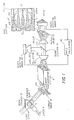
- Fig. 1 is a simplified partly perspective schematic view of an improved wavefront sensor according to this invention with an enlarged view of one cell 100 of filter array 10.
- Fig. 2 is a perspective view of the prior art I3 sensor taken from Fig. 6 of U. S. Patent No. 4,141,652.
- Fig. 3 is a perspective view of the prior art wavefront sensor taken from Fig. 1 of U. S. Patent No. 4,399,356.
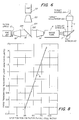
- Fig. 4 is a front view of one filter cell 100 in accordance with the invention.
- Fig. 5 is a front view of a filter array 10 in accordance with the invention.
- Fig. 6 is a schematic of a test system used to simulate the invention.
- Fig. 7 A-E show alternate embodiments of filter cells.
- Fig. 8 is a plot of wavefront sensor output versus spot position for a prototype filter array.
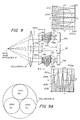
- Fig. 9 is a schematic of a two wavefront sensor in accordance with the invention.
- Fig. 9A is a front view in the direction of lines 9-9 of Fig. 9.
- Fig. 10 is an alternate embodiment of a two axis wavefront sensor.
- Fig. 11 is a further alternate embodiment of a filter mask using different colored mask chevrons.
- Fig. 12 is a schematic illustrating use of the mask of Fig. 11.
- Fig. 13 is a partial plan view of a filter mask cell 100G in which the transmittance characteristics are variable.
- Fig. 14 is a sectional schematic view of an embodiment of the invention wherein the filter array is incorporated into the screen of an image intensifier.
- Fig. 15 is a plan view of the conductive screen mask of Fig. 13.
- a light beam 8 is shown entering the optical system.
- Light beam 8 may be a wavefront of light originating from a distant object, for example, a satellite or star, or may be light reflected from an object illuminated by a source located in proximity to the apparatus of Fig. 1.
- beam 8 may be combined in beam combiner 2 with a reference light beam 9 from laser 6.
- the optional reference beam 9 is preferably an amplitude modulated plane or spherical wavefront emitted by a laser source modulated by an acousto-optical modulator (not shown).
- Reference beam 9 provides an optical and electronic self-calibration feature for wavefront tilt measurement.
- the object of the system of Fig. 1 is to sense the shape of the optical wavefront of beam 8 at relatively high speeds approaching real-time. Once sensed, the measurements can be used prior to imaging the beam to correct the wavefront for atmospheric aberrations or other undesired perturbations, as described in U. S. Patent No. 4,399,356.
- the combined beam 7 from beam combiner 2 is imaged on lenslet array 12 which may comprise a two-dimensional array of individual lenses which divide the beam 7 into a plurality of subaperture beams 120 which are focused on image intensifier 4 forming a plurality of light spots thereon.
- Image intensifier 4 amplifies the intensity of each subaperture spot impinging on the face of the intensifier.
- the amplified subaperture images are collimated by collimator 14 and focused by lens system 18 onto the individual cells 100 of filter array 10.
- variable transmission filter 10 is placed after the image intensifier 4.
- This intensifier 4 produces enough gain to allow the output light to split between detectors without degrading overall performance. There is, however, a penalty to be paid in using the intensifier 4, since it is not a perfect amplifier and may introduce some noise into the target spot image. However, this intensifier generated noise may be made insignificant by increasing the intensifer gain and thus producing large photon fluxes on the mask array.
- Filter array 10 is a mask having as many mask cells 100 as beam subapertures. Each subaperture spot 200 is focused onto an individual mask cell 100. As shown in the enlarged view of Fig. 1, each cell 100 has a linearly variable light transmission characteristic along one direction of spot motion. In the example of Fig. 1, the variable light transmission characteristic is horizontal, i.e., along the X-axis of the cell 100.
- the spot labelled 200 in solid lines is centered on the cell 100 and represents the spot produced by the untilted reference beam wavefront 9.
- the spot 200(a) represents the spot from a subaperture of the beam which is tilted in the positive X-direction.
- the cell mask may be seen to comprise a plurality of alternate opaque and transparent elongated V-shaped patterns, or chevrons, 210 and 212, respectively, arranged such that the Y-dimension of the opaque chevrons 210 are wider in the minus X-direction and linearly diminish toward the plus X-direction while the converse applies to the transparent chevrons 212.
- a comparison of the centered spot 200 and shifted spot 200 (a) vis-a-vis the chevroned mask reveals that the intensity of the light detected at photodetector 24 from cell 100 is greater for spot 200 (a) than for spot 200 (assuming they were of equal intensity to begin with) since less of the spot 200 (a) is intersected by the opaque chevron 210 than is the case with the centered spot 200.
- a spot shifted in the minus X-direction is more attenuated by the opaque chevrons 210 resulting in a lower light intensity, as detected by photodetector 24.
- filter array 10 in a simple analog manner. Summing of the weighted pixels is accomplished by detector 24 which may comprise a plurality of photo-diodes 24 (a) (one for each cell) in an array. The photo-diodes 24 (a) integrate the intensity of each detected subaperture pixel received over the whole area of the photodetector.
- the output intensity sensed by each photo-diode 24 (a) is proportional to the horizontal spot position on each cell 100 of the variable transmission filter mask 10.
- the intensity is measured by a second detector array 22, that senses the subapertured input beam 122 after it is partially reflected by beam splitter 16.
- a ratio is constructed in calculator 28 of the transmitted light intensity sensed by detector array 24 versus the input intensity sensed by detector array 22. That ratio varies in response to spot motion.
- lens 18 it may be advantageous to utilize lens 18 to spread the subaperture images from collimator 14 instead of simply focusing such images onto cells 100, as described above. In this manner, the spot size on the cell is increased and the light is spread over a larger portion of the cell to yield greater linearity.
- the heart of the wavefront sensor system of the invention is the filter array 10. It is this filter that accomplishes the pixel weight multiplication for the centroid calculation. Therefore, the performance of the wavefront sensor depends critically upon how well this filter can apply the requisite linear weighting of intensity. Filters exist which have variable density characteristics achieved by forming evaporated metallic films of variable thickness. With present known technology, the linearity of such filters is at most about 2%; which would introduce intolerable errors for most foreseeable applications of the present system. For this reason, a binary mask in the form of only opaque and transparent regions with no partially transmitting regions is believed to be preferable over a variable thickness filter.
- the V-shaped patterns quite small in the vertical dimension, i.e., 10 to 20 microns, to assure that the spot covers many chevrons, thus averaging out any errors that may occur by spot motion in the vertical or Y-direction.
- the size of the mask cell 100 should also be commensurate with the subaperture size of the lenslet array 12 used to divide the input pupil into subapertures.
- a test cell consisting of 500 micron square cells comprising fifty 10 micron by 500 micron, opaque chevrons, as shown in Fig. 4, was constructed and replicated in a 5 x 5 array on 500 micron centers, as shown in Fig. 5. Note that for simplicity, only 5 opaque chevrons 212 are shown per cell and that figures 4 and 5 are not to scale. In actuality the horizontal scale of the chevrons is much greater.
- the test cell was constructed from a glass substrate upon which a thin film chrome coating was formed. Chevron-shaped opaque chrome elements were formed by etching the chrome film. The chevron element had a base width of 10 microns which linearly diminished to a point of 0.5 microns over a length of 500 microns to produce a transmission profile across the horizontal length of the cell which varies linearly from 0% to 100%.
- test filter 10 of Fig. 5 was tested in the optical system of Fig. 6 which simulates the embodiment of Fig. 1. Note similar parts contain the same reference numerals in each of figures 1 and 6.
- the target source 64 produces a beam 7 which is collimated by collimator 62.
- the wavefront tilt of the beam may be changed by a 2-axis adjustable tilt mirror 60.
- the tilted collimated beam 7 is coupled to a lenslet array 12, which produces diffraction limited blur spots upon the photocathode of the image tube 4.
- the intensified blur spot array that appears at the output phosphor screen of the image tube is collimated by a fast (f/0.95) lens 14.
- This intensified collimated beam 122 passes through a partially reflective beam splitter 16 which sends 30% of the light to the photo-multiplier tube (PMT) 22 that represents the denominator channel of the ratio calculation of the wavefront sensor.
- PMT photo-multiplier tube
- the 70% transmitted beam 126 enters an identical f/0.95 lens 18 and the spots are imaged onto the filter array 10.
- the light transmitted by the filter 10 is detected by the second PMT 24.
- the output signals from the two PMTs represent the incident and transmitted beams of the wavefront sensor.
- This optical system was operated in two modes.
- the target source simulator 64 was operated to produce high light levels.
- the output currents of the two PMTs 22 and 24 were recorded as the wavefront tilt was changed. Because the photon flux at the filter array 10 was very high in this first mode (on the order of 106 photons/sec.), this mode allowed testing of the filter 10 without considering the added noise due to photon statistics.
- Fig. 8 is a plot of the ratio of the transmitted to incident light versus the spot position on the filter of a typical data set obtained as the spots were moved through one cell of the filter. Fitting a linear relation line A to the central portion of the data shows that the RMS errors in the tilt predicted by the system are 0.6% over a dynamic range of 3.2 waves of tilt of the input beam. The somewhat restricted dynamic range indicated is believed due, in part, to the spillover of light from adjacent subapertures or cells. The linearity errors are believed mainly due to random errors in the PMT data recording system which includes an eight-bit A/D converter.
- the spillover problem may be alleviated by utilizing a mask cell, as shown in Fig. 7a, with an opaque border 115 around each cell 100′.
- the light level of the target source simulator 64 was reduced to the level at which it became possible to detect individual intensified photons at the PMTs 22 and 24.
- the charge pulses from the PMTs were integrated, digitized and ratioed singly, allowing the data to be accumulated a single input photon at a time.
- the error in the accumulated centroid measurement was monitored as a function of photon number. In this case, the centroid error was found to be photon statistics limited because the digitizer error had been eliminated. It was found that the required centroid accuracy could be achieved with less than 300 detected input photons and an image tube gain of 12600.
- the linearity of the filter 10 was found to be better than 0.3%, close to that predicted by numeric calculations.
- the wavefront sensor previously described in connection with Fig. 1, is only useful in determining wavefront tilt in a single axis since the transmission characteristics of the filter array cells only vary linearly in one axis, i.e., the horizontal or X-axis.
- the beam from collimator 14 of Fig. 1 is divided into three separate beams.
- three re-imagers 18X, 18Y and 20 are placed in the path of the image intensifier beam after it has been collimated by collimator 14.
- the re-imagers are arranged in a triangular area to tri-sect the collimated beam.
- the collimated beam is effectively divided into three identical separate beams 122(a), (b) and (c), which impinge on lenses 18X, 20 and 18Y, respectively.
- the image beam from lens 18 is projected onto the X coordinate weighting mask array 10X which is identical to the mask 10 of Fig. 1 and processed as in Fig. 1.
- the reference beam 124 is imaged by lens 20 directly onto photodetector array 22, also as described in connection with Fig. 1.
- the additional Y-axis beam channel is provided by projecting the third beam 122(c) onto the Y-coordinate weighting mask array 10Y via lens 18Y.
- Mask array 10Y is identical to mask array 10X except that the chevrons 212Y and 210Y of each cell 100Y are oriented 90° from those of cell 100X, as shown in the enlarged view.
- a bundle of tapered fiber optic plugs 90X, 90Y may be provided between the mask 10X; mask 10Y, respectively, to provide image reduction where the filter cell size cannot be made small enough to mate directly with the pixel size of detectors 24 and 24Y.
- a spot motion in the vertical or Y direction is weighted by mask 10Y in the same manner as previously described in connection with Fig. 1.
- the weighted pixel intensity from the mask is detected by photodetector array 24Y and ratioed with the unweighted reference beam intensity determined by photodetector array 24Y.
- FIG. 10 An alternate two axis wavefront sensor is shown in simplified schematic form in Fig. 10 wherein like parts contain identical numeral designations.
- a three faceted mirror pyramid 500 is placed in the image plane of the collimated beam 122 from image intensifier 4 to divide the beam into three beams 122a, 122b and 122c, each smaller than the collimated beam produced by collimator 14.
- This embodiment has an advantage in that the focal lengths of the re-imaging lenses 18X, 18Y and 20 can be shorter than that of the collimator 14, thereby providing a linear scale reduction.
- a third alternative for beam splitting is to simply utilize a second beam splitter 16 in addition to that shown in Fig. 1 to provide threeway division.
- the disadvantage of this structure is that the re-imaging lenses must be able to accommodate the full collimated beam size. Since the collimator must be an exceptionally fast lens, the beam diameter is large compared to the collimator focal length. Therefore, if the re-imagers are to accept this full beam, their focal lengths cannot be much different from that of the collimator. Since the magnification of the system is set by the ratio of these focal lengths, this splitting method does not allow minification of the spots onto the filters; as may be required if the detector diodes are smaller than the mask cell size.
- FIG. 11 Another class of mask cells comprise patterns which are not wholly opaque, as shown in Fig. 11.
- the chevron mask cells in Fig. 11 have chevrons C1 and C2 that selectively transmit various wavelengths of light.
- the C1 chevrons absorb light in the red wavelength
- the C2 chevrons absorb light in the blue wavelength.
- the mask cell 100F may be used to calculate, for example, the centroid of the distributions of only those wavelengths of light at which the chevrons are opaque.
- One use of such a mask would be for a two-axis centroid calculation, in the form of two chevron patterns, C1 and C2, of differing wavelength opacity characteristics placed at 90° to each other in the same mask cell, as shown in Fig. 11.
- the transmitted light is sensed by two detectors, D1 and D2 (Fig. 12) with optical transmission filters matched in wavelength to the two chevron patterns C1 and C2.
- the centroid of a white light spot may be sensed in both axes with only one filter mask array.
- filter masks whose transmittance characteristics may be electrically varied.
- Such a mask may be fabricated of liquid crystal devices (LCD's) as shown in Fig. 13 wherein the opacity of each LCD may be electrically varied by row and column electronic impulses. In this way, the weighting applied to a given pixel may be varied in response to an external signal.
- LCD's liquid crystal devices
- the cell 100G comprises opaque chevrons C13 approximated by enabling selected LCD's from the an NXM array of LCD's.
- FIG. 14 and 15 An analogous class of embodiments is contemplated in which the masks are embodied in electron optical systems rather than in photon optical systems.
- the phosphor output screen of a well-known image intensifier 400 is replaced by an array 101 of electrically conductive chevron patterns C14 (Fig. 15) forming cells 100H.
- the centroid calculation is performed directly on the electron image that is present at that position.
- lenslet array 12′ is focused on a spot imager 401 comprising a fiber optic input window coupling the light spots directly to photocathode 402.
- Accelerating electrode 405 increases the energy of the electron beam and electron lens 404 focuses the electronic beam from the photocathode onto the electrically conductive mask 10′ to produce an intensified electrical signal output from the mask which represents the spot intensity from each subaperture encoded by a function proportional to the electron collecting pattern of the conductive mask.
- optical embodiments of the invention may be similarly converted to analogous electronic optical arrangements.
- Such systems should provide simplifications of the optical layout of a wavefront sensing apparatus.
- a micro-channel-plate electron multiplier may be substituted for the accelerating electrode 405 in Fig. 14.
- the optical embodiments herein utilize the transmission characteristics of an optical mask to encode a function of spot intensity distribution. It is contemplated that the reflective characteristics of a photomask may be used equally as well. Accordingly, in the claims, the broader term "directivity" characteristics will be used to encompass either case.
Landscapes
- Physics & Mathematics (AREA)
- General Physics & Mathematics (AREA)
- Spectroscopy & Molecular Physics (AREA)
- Optics & Photonics (AREA)
- Photometry And Measurement Of Optical Pulse Characteristics (AREA)
- Microscoopes, Condenser (AREA)
- Instruments For Measurement Of Length By Optical Means (AREA)
- Investigating Or Analysing Materials By Optical Means (AREA)
- Facsimile Scanning Arrangements (AREA)
Claims (20)
- Optische Wellenfront-Fühlereinrichtung zur Bestimmung einer Wellenfrontabweichung in einem Lichtstrahl, mit- Strahlteilermitteln (12) zur Unterteilung des Lichtstrahls in eine Mehrzahl von Teilaperturkomponenten (120) des Lichtes;- Detektormitteln (24) zur Bestimmung der Signalintensität entsprechend der Lichtintensität, die von jeder Teilaperturkomponente (120) ausgeht;- Abbildungsmitteln (14, 18) zur Signalübertragung zwischen den genannten Strahlteilermitteln (12) und den Detektormitteln (24), sowie Bildinformations-Verstärkermitteln (4), welche auf das Licht von jeder Teilaperturkomponente (120) ansprechen, um die Signalintensität entsprechend dem Licht von jeder Teilaperturkomponente (120) zu erhöhen,dadurch gekennzeichnet, daß
eine Filterreihenanordnung (10) vorgesehen ist, die zwischen den Bildinformations-Verstärkermitteln (4) und den Detektormitteln (24) angeordnet ist und eine Anzahl von Zellen (100) enthält, die jeweils eine Richtcharakteristik aufweisen, die sich in mindestens einer Richtung einer Bildpunktbewegung der Abbildungsmittel (14, 18) verändert. - Fühlereinrichtung nach Anspruch 1,
dadurch gekennzeichnet, daß
die genannte Filterreihenanordnung (10) eine Filtermaskenanordnung mit einer Anzahl von Maskenzellen (100) ist, daß die Abbildungsmittel optische Abbildungsmittel sind und daß die Bildinformations-Verstärkermittel Bildverstärkermittel sind, welche ein verstärktes optisches Bild liefern. - Fühlereinrichtung nach Anspruch 1 oder 2
dadurch gekennzeichnet, daß
die genannte Richtcharakteristik jeder der genannten Zellen (100) der Filterreihenanordnung (10) eine lineare Funktion ist. - Fühlereinrichtung nach Anspruch 1 oder 2,
dadurch gekennzeichnet, daß
die genannte Richtcharakteristik jeder der genannten Zellen (100) der Filterreihenanordnung (10) eine quadratische Funktion ist. - Fühlereinrichtung nach Anspruch 1 oder 2,
dadurch gekennzeichnet, daß
die genannte Richtcharakteristik jeder der genannten Zellen (100) der Filterreihenanordnung (10) eine Funktion des Quadrates des Abstandes über die Zelle hin in einer vorbestimmten Richtung ist. - Fühlereinrichtung nach Anspruch 1 oder 2,
dadurch gekennzeichnet, daß
die genannte Richtcharakteristik jeder der genannten Zellen (100) der Reihenanordnung (10) sich als eine lineare Funktion der radialen Ablage von dem Zentrum jeder der genannten Zellen (100) ändert. - Fühlereinrichtung nach Anspruch 2,
dadurch gekennzeichnet, daß
jede Maskenzelle eine lineare Reihe sich abwechselnder undurchsichtiger und transparenter Streifen aufweist und daß die Richtcharakteristik das Transmissionsverhalten ist. - Fühlereinrichtung nach Anspruch 2,
dadurch gekennzeichnet, daß
jede Maskenzelle eine lineare Reihe abwechselnd undurchsichtiger und transparenter paralleler Linien aufweist. - Fühlereinrichtung nach Anspruch 2,
dadurch gekennzeichnet, daß
jede Maskenzelle eine lineare Reihe von abwechselnd undurchsichtigen und transparenten Kreisen aufweist. - Fühlereinrichtung nach einem der Ansprüche 2 oder 7 bis 9,
dadurch gekennzeichnet, daß
die genannte Filtermaskenanordnung (10) Maskenzellen aufweist, deren Richtcharakteristik elektrisch veränderbar ist. - Fühlereinrichtung nach einem der Ansprüche 1 bis 10,
dadurch gekennzeichnet, daß
die genannte Filterreihenanordnung (10) zwei Gruppen von Zellen enthält, wobei die Richtcharakteristik einer Gruppe dieser Zellen sich in einer ersten Richtung verändert und die Richtcharakteristik der zweiten Gruppe sich in einer hierzu senkrechten Richtung ändert. - Fühlereinrichtung nach einem der Ansprüche 1 bis 11,
dadurch gekennzeichnet, daß
die genannten Strahlteilermittel (12) eine Gruppe von kleinen Linsen enthalten, die in dem Weg des Strahles angeordnet sind. - Fühlereinrichtung nach einem der Ansprüche 1 bis 12,
dadurch gekennzeichnet, daß
zusätzlich zu den genannten Detektormitteln (24) zweite Detektormittel (22) zur Bestimmung der Lichtintensität vorgesehen sind, die unmittelbar aus den genannten Bildinformations-Verstärkermitteln (4) empfangen wird, und daß Rechnermittel (28) zur Berechnung des Verhältnisses des Signales aus den erstgenannten Detektormitteln (24) und des Signales aus den genannten zweiten Detektormitteln (22) dienen. - Fühlereinrichtung nach einem der Ansprüche 1 oder 3 bis 6,
dadurch gekennzeichnet, daßa) die genannten Bildinformations-Verstärkermittel (4) eine Linse (401) zur Abbildung der Teilaperturen (120), photoelektronische Mittel (402), die auf das abgebildete Licht von jeder Teilaperturkomponente (120) ansprechen, um das genannte abgebildete Licht in Elektronenstrahlen umzuwandeln, sowie Mittel enthalten, um die in jedem Elektronenstrahl enthaltene Energie zu erhöhen;b) die genannte Filterreihenanordnung (10) gegenüber Elektronen empfindliche Mittel enthält, um die räumliche Verteilung der Energie in den genannten Elektronenstrahlen zu bestimmen; undc) die genannten Detektormittel (24) elektronische Mittel enthalten, um die Wellenfrontabweichung aus dem Ansprechen der genannten, gegenüber Elektronen empfindlichen Mittel zu bestimmen. - Fühlereinrichtung nach Anspruch 14,
dadurch gekennzeichnet, daß
die genannten photoelektronischen Mittel aus einer Photokathode bestehen. - Fühlereinrichtung nach Anspruch 14 oder 15,
dadurch gekennzeichnet, daß
die energieverstärkenden Mittel in einem elektronischen Beschleunigungspotential bestehen. - Fühlereinrichtung nach Anspruch 14 oder 15,
dadurch gekennzeichnet, daß
die genannten energieverstärkenden Mittel in einem Mikrokanalplatten-Elektronenvervielfacher bestehen. - Fühlereinrichtung nach einem der Ansprüche 14 bis 17,
dadurch gekennzeichnet, daß
die gegenüber Elektronen empfindlichen Mittel aus leitfähigen Elektroden in einem Maskenmuster bestehen, das in dem Weg der Elektronenstrahlen angeordnet ist. - Fühlereinrichtung nach einem der Ansprüche 14 bis 17,
dadurch gekennzeichnet, daß
die genannten, gegenüber Elektronen empfindlichen Mittel in einer Gruppe von Siliziumdioden bestehen. - Verfahren zur Bestimmung einer Wellenfrontabweichung in einem Eingangslichtstrahl, wobei ein modulierter Bezugslichtstrahl mit dem genannten Eingangslichtstrahl kombiniert wird, um einen kombinierten Strahl zu bilden, der in eine Anzahl von Teilaperturkomponenten (120) aufgeteilt wird, die durch Detektormittel (24) detektiert werden, und wobei die Wellenfrontabweichung aus dem Ausgang dieser Detektormittel (24) bestimmt wird,
dadurch gekennzeichnet, daßa) die Teilaperturkomponenten (120) optisch oder elektronisch verstärkt werden;b) die genannten verstärkten Teilaperturkomponenten (120) optisch oder elektronisch auf eine Filterreihenanordnung (10) abgebildet werden, welche Zellen aufweist, die jeweils eine Richtcharakteristik haben, die sich in mindestens einer Richtung der Abbildungspunktbewegung ändert; undc) die Wellenfrontabweichung aus dem Ausgang jeder der genannten Zellen der Filterreihenanordnung (10) bestimmt wird.
Applications Claiming Priority (2)
| Application Number | Priority Date | Filing Date | Title |
|---|---|---|---|
| US736933 | 1985-05-22 | ||
| US06/736,933 US4725138A (en) | 1985-05-22 | 1985-05-22 | Optical wavefront sensing system |
Publications (3)
| Publication Number | Publication Date |
|---|---|
| EP0203530A2 EP0203530A2 (de) | 1986-12-03 |
| EP0203530A3 EP0203530A3 (en) | 1989-07-12 |
| EP0203530B1 true EP0203530B1 (de) | 1995-02-01 |
Family
ID=24961934
Family Applications (1)
| Application Number | Title | Priority Date | Filing Date |
|---|---|---|---|
| EP86106964A Expired - Lifetime EP0203530B1 (de) | 1985-05-22 | 1986-05-22 | Vorrichtung zur Abtastung einer optischen Wellenfront |
Country Status (4)
| Country | Link |
|---|---|
| US (1) | US4725138A (de) |
| EP (1) | EP0203530B1 (de) |
| AT (1) | ATE118092T1 (de) |
| DE (1) | DE3650220T2 (de) |
Cited By (1)
| Publication number | Priority date | Publication date | Assignee | Title |
|---|---|---|---|---|
| DE102008016767A1 (de) * | 2008-04-02 | 2009-11-19 | Sick Ag | Optoelektronischer Sensor und Verfahren zur Detektion von Objekten |
Families Citing this family (62)
| Publication number | Priority date | Publication date | Assignee | Title |
|---|---|---|---|---|
| US4967063A (en) * | 1988-06-16 | 1990-10-30 | The Aerospace Corporation | Charge controlled adaptive-optics system |
| US4935614A (en) * | 1989-04-05 | 1990-06-19 | The Charles Stark Draper Laboratory, Inc. | Real-time wavefront sensor for coherent wavefront characterization |
| US5026977A (en) * | 1989-04-05 | 1991-06-25 | The Charles Stark Draper Laboratory, Inc. | Wavefront sensing and correction with deformable mirror |
| US4967077A (en) * | 1989-05-09 | 1990-10-30 | The United States Of America As Represented By The Secretary Of The Air Force | Multiple aperture arrays for optical and radio frequency signals |
| US4943709A (en) * | 1989-05-11 | 1990-07-24 | Hughes Aircraft Company | Liquid crystal adaptive optics system |
| DE4003698C2 (de) * | 1990-02-07 | 1994-09-08 | Wild Heerbrugg Ag | Wellenfrontsensor |
| US5083015A (en) * | 1990-11-16 | 1992-01-21 | United Technologies Corporation | Optical centroid processor wavefront sensor |
| US5124542A (en) * | 1990-11-30 | 1992-06-23 | Eastman Kodak Company | Method for quantitatively determining petal piston in a segmented imaging assembly |
| US5164578A (en) * | 1990-12-14 | 1992-11-17 | United Technologies Corporation | Two-dimensional OCP wavefront sensor employing one-dimensional optical detection |
| US5120128A (en) * | 1991-01-14 | 1992-06-09 | Kaman Aerospace Corporation | Apparatus for sensing wavefront aberration |
| US5118935A (en) * | 1991-02-28 | 1992-06-02 | Eastman Kodak Company | Composite imaging mask |
| US5120948A (en) * | 1991-02-28 | 1992-06-09 | Eastman Kodak Company | Method for simultaneously determining coarse and fine petal piston in a segmented imaging assembly |
| US5287165A (en) * | 1991-09-30 | 1994-02-15 | Kaman Aerospace Corporation | High sensitivity-wide dynamic range optical tilt sensor |
| US5600123A (en) * | 1993-02-17 | 1997-02-04 | Litton Systems, Inc. | High-resolution extended field-of-view tracking apparatus and method |
| US5412200A (en) * | 1993-03-01 | 1995-05-02 | Rhoads; Geoffrey B. | Wide field distortion-compensating imaging system and methods |
| US6084227A (en) * | 1995-01-30 | 2000-07-04 | Rhoads; Geoffrey B. | Method and apparatus for wide field distortion-compensated imaging |
| US5448053A (en) * | 1993-03-01 | 1995-09-05 | Rhoads; Geoffrey B. | Method and apparatus for wide field distortion-compensated imaging |
| WO1995034800A1 (en) * | 1994-06-14 | 1995-12-21 | Visionix Ltd. | Apparatus for mapping optical elements |
| US5629765A (en) * | 1995-12-15 | 1997-05-13 | Adaptive Optics Associates, Inc. | Wavefront measuring system with integral geometric reference (IGR) |
| US5936720A (en) * | 1996-07-10 | 1999-08-10 | Neal; Daniel R. | Beam characterization by wavefront sensor |
| FR2759208B1 (fr) * | 1997-01-31 | 1999-05-07 | Thomson Csf | Dispositif de controle du pointage et de la focalisation des chaines laser sur une cible |
| US6121953A (en) * | 1997-02-06 | 2000-09-19 | Modern Cartoons, Ltd. | Virtual reality system for sensing facial movements |
| US6219360B1 (en) | 1998-04-24 | 2001-04-17 | Trw Inc. | High average power solid-state laser system with phase front control |
| US6819414B1 (en) | 1998-05-19 | 2004-11-16 | Nikon Corporation | Aberration measuring apparatus, aberration measuring method, projection exposure apparatus having the same measuring apparatus, device manufacturing method using the same measuring method, and exposure method |
| US6007204A (en) * | 1998-06-03 | 1999-12-28 | Welch Allyn, Inc. | Compact ocular measuring system |
| US6791696B1 (en) | 1998-06-18 | 2004-09-14 | Optikos Corporation | Automated optical measurement apparatus and method |
| GB9820664D0 (en) * | 1998-09-23 | 1998-11-18 | Isis Innovation | Wavefront sensing device |
| US6750958B1 (en) | 1999-06-09 | 2004-06-15 | Optikos Corporation | Automated optical measurement apparatus and method |
| FR2796167A1 (fr) * | 1999-07-06 | 2001-01-12 | Thomson Csf | Systeme optique de conversion d'un front d'onde equi-energie en front d'onde d'energie variable |
| US6304330B1 (en) | 1999-10-06 | 2001-10-16 | Metrolaser, Inc. | Methods and apparatus for splitting, imaging, and measuring wavefronts in interferometry |
| US6707020B1 (en) * | 1999-12-28 | 2004-03-16 | Mza Associates Corporation | Adaptive dynamic range wavefront sensor |
| US7455407B2 (en) * | 2000-02-11 | 2008-11-25 | Amo Wavefront Sciences, Llc | System and method of measuring and mapping three dimensional structures |
| US6550917B1 (en) | 2000-02-11 | 2003-04-22 | Wavefront Sciences, Inc. | Dynamic range extension techniques for a wavefront sensor including use in ophthalmic measurement |
| EP1277172A2 (de) | 2000-04-25 | 2003-01-22 | Alcon Universal, Ltd. | Raumfilterverfahren und -vorrichtung zur verbesserung von hartman-shack bildern |
| US6565209B2 (en) | 2000-04-25 | 2003-05-20 | Alcon Universal Ltd. | Range-extending system and spatial filter for enhancing Hartmann-Shack images and associated methods |
| US7161128B2 (en) * | 2000-07-14 | 2007-01-09 | Adaptive Optics Associates, Inc. | Optical instrument employing a wavefront sensor capable of coarse and fine phase measurement capabilities during first and second modes of operation |
| US6649895B1 (en) | 2000-07-14 | 2003-11-18 | Adaptive Optics Associates, Inc. | Dispersed Hartmann sensor and method for mirror segment alignment and phasing |
| US6486943B1 (en) | 2000-09-19 | 2002-11-26 | The Schepens Eye Research Institute, Inc. | Methods and apparatus for measurement and correction of optical aberration |
| US6548797B1 (en) | 2000-10-20 | 2003-04-15 | Nikon Corporation | Apparatus and method for measuring a wavefront using a screen with apertures adjacent to a multi-lens array |
| JP4199000B2 (ja) | 2001-03-15 | 2008-12-17 | エイエムオー・ウェーブフロント・サイエンシーズ・リミテッド・ライアビリティ・カンパニー | 光学システムをマッピングするための断層撮影波面分析システム及び方法 |
| US6582079B2 (en) | 2001-06-05 | 2003-06-24 | Metrologic Instruments, Inc. | Modular adaptive optical subsystem for integration with a fundus camera body and CCD camera unit and improved fundus camera employing same |
| FR2827380B1 (fr) * | 2001-07-12 | 2003-11-07 | Imagine Optic | Dispositif d'analyse d'un front d'onde a resolution amelioree |
| US6709108B2 (en) | 2001-08-31 | 2004-03-23 | Adaptive Optics Associates, Inc. | Ophthalmic instrument with adaptive optic subsystem that measures aberrations (including higher order aberrations) of a human eye and that provides a view of compensation of such aberrations to the human eye |
| US6674519B2 (en) | 2001-12-21 | 2004-01-06 | Northrop Grumman Corporation | Optical phase front measurement unit |
| DE10316123A1 (de) | 2003-04-04 | 2004-10-14 | Carl Zeiss Smt Ag | Vorrichtung und Verfahren zur Wellenfrontvermessung eines optischen Abbildungssystems durch phasenschiebende Interferometrie |
| US7002750B2 (en) * | 2003-11-06 | 2006-02-21 | Ann-Lun Lee | Image capturing device |
| US7343099B2 (en) * | 2004-02-12 | 2008-03-11 | Metrologic Instruments, Inc. | Free space optical (FSO) laser communication system employing fade mitigation measures based on laser beam speckle tracking and locking principles |
| US20050243275A1 (en) * | 2004-04-30 | 2005-11-03 | Curatu Eugene O | Wavefront sensor and relay for optical measurement and associated methods |
| US20060186312A1 (en) * | 2005-02-23 | 2006-08-24 | Zino Altman | Apparatus and method for optical wavefront analysis using active light modulation |
| US7268937B1 (en) | 2005-05-27 | 2007-09-11 | United States Of America As Represented By The Secretary Of The Air Force | Holographic wavefront sensor |
| CN100573065C (zh) * | 2006-08-07 | 2009-12-23 | 中国科学院光电技术研究所 | 一种基于线性相位反演的波前测量方法 |
| EP2403396B1 (de) * | 2009-03-04 | 2019-08-14 | Elie Meimoun | Vorrichtung und verfahren zur überprüfung von wellenfrontanalysen |
| GB2468911A (en) * | 2009-03-27 | 2010-09-29 | Light Blue Optics Ltd | Aberration correction methods using wavefront sensing hologram patches and mapping of phase aberration corrections |
| CN102073136B (zh) * | 2010-12-24 | 2012-07-25 | 中国科学院长春光学精密机械与物理研究所 | 液晶自适应光学系统能量优化分配方法 |
| GB2493729A (en) * | 2011-08-16 | 2013-02-20 | Bae Systems Plc | Infra red wavefront sensor device with tapered fibre optic image conduits |
| JP6080427B2 (ja) * | 2012-08-10 | 2017-02-15 | キヤノン株式会社 | シャック・ハルトマンセンサとそれを利用した波面計測方法 |
| DE102014010667B4 (de) | 2014-07-18 | 2017-07-13 | Berliner Glas Kgaa Herbert Kubatz Gmbh & Co | Verfahren und Vorrichtung zur Messung der Form einer Wellenfront eines optischen Strahlungsfeldes |
| US11143386B2 (en) | 2017-06-01 | 2021-10-12 | Signify Holding B.V. | Collimator device, a lighting device, a lamp and a luminaire |
| US10962474B2 (en) * | 2018-05-24 | 2021-03-30 | Regents Of The University Of Minnesota | Optical aberration detection systems |
| DE102019009150A1 (de) * | 2019-01-14 | 2020-08-20 | Dioptic Gmbh | Wellenfrontsensor |
| US10641897B1 (en) * | 2019-04-24 | 2020-05-05 | Aeye, Inc. | Ladar system and method with adaptive pulse duration |
| CN114911053B (zh) * | 2022-07-14 | 2022-10-28 | 中国科学院长春光学精密机械与物理研究所 | 一种多级串行系统及其工作方法 |
Family Cites Families (17)
| Publication number | Priority date | Publication date | Assignee | Title |
|---|---|---|---|---|
| US3551681A (en) * | 1964-09-04 | 1970-12-29 | Barnes Eng Co | Non-scanning horizon position indicator independent of planet radiance variations utilizing inverted overlapping fields of view |
| US3731103A (en) * | 1971-02-24 | 1973-05-01 | Hughes Aircraft Co | Adaptive arrays |
| US3861801A (en) * | 1973-06-18 | 1975-01-21 | Perkin Elmer Corp | Device for sampling laser beams |
| US3904274A (en) * | 1973-08-27 | 1975-09-09 | Itek Corp | Monolithic piezoelectric wavefront phase modulator |
| US3923400A (en) * | 1974-01-03 | 1975-12-02 | Itek Corp | Real-time wavefront correction system |
| US4016415A (en) * | 1974-06-24 | 1977-04-05 | Hughes Aircraft Company | Adaptive imaging telescope with linear sensing and movable mirror phase shifting |
| US3988608A (en) * | 1974-06-24 | 1976-10-26 | Hughes Aircraft Company | Adaptive imaging telescope with nonlinear sensing and electro-optical phase shifting |
| US3980879A (en) * | 1974-06-24 | 1976-09-14 | Hughes Aircraft Company | Adaptive imaging telescope with nonlinear quadrant sensing and electro-optical phase shifting |
| US3975629A (en) * | 1974-06-24 | 1976-08-17 | Hughes Aircraft Company | Adaptive imaging telescope with linear sensing and electro-optical phase shifting |
| US3979585A (en) * | 1974-06-24 | 1976-09-07 | Hughes Aircraft Company | Adaptive imaging telescope with camera-computer transform image quality sensing and electro-optic phase shifting |
| US4141652A (en) * | 1977-11-25 | 1979-02-27 | Adaptive Optics Associates, Inc. | Sensor system for detecting wavefront distortion in a return beam of light |
| US4248504A (en) * | 1978-12-08 | 1981-02-03 | Itek Corporation | Piezoelectric wavefront modulator |
| US4399356A (en) * | 1981-01-19 | 1983-08-16 | Adaptive Optics Associates, Inc. | Optical wavefront sensing system |
| US4441019A (en) * | 1982-01-28 | 1984-04-03 | Itek Corporation | Wavefront sensor with astigmatic optics |
| US4438330A (en) * | 1982-03-01 | 1984-03-20 | Itek Corporation | Wavefront sensor employing a modulation reticle |
| US4472029A (en) * | 1982-03-01 | 1984-09-18 | Itek Corporation | Integrated wavefront compensator |
| US4575248A (en) * | 1984-06-18 | 1986-03-11 | Itek Corporation | Wavefront sensor employing novel D.C. shearing interferometer |
-
1985
- 1985-05-22 US US06/736,933 patent/US4725138A/en not_active Expired - Lifetime
-
1986
- 1986-05-22 AT AT86106964T patent/ATE118092T1/de active
- 1986-05-22 EP EP86106964A patent/EP0203530B1/de not_active Expired - Lifetime
- 1986-05-22 DE DE3650220T patent/DE3650220T2/de not_active Expired - Fee Related
Cited By (2)
| Publication number | Priority date | Publication date | Assignee | Title |
|---|---|---|---|---|
| DE102008016767A1 (de) * | 2008-04-02 | 2009-11-19 | Sick Ag | Optoelektronischer Sensor und Verfahren zur Detektion von Objekten |
| DE102008016767B4 (de) * | 2008-04-02 | 2016-07-28 | Sick Ag | Optoelektronischer Sensor und Verfahren zur Detektion von Objekten |
Also Published As
| Publication number | Publication date |
|---|---|
| US4725138A (en) | 1988-02-16 |
| DE3650220D1 (de) | 1995-03-16 |
| DE3650220T2 (de) | 1995-06-22 |
| EP0203530A3 (en) | 1989-07-12 |
| EP0203530A2 (de) | 1986-12-03 |
| ATE118092T1 (de) | 1995-02-15 |
Similar Documents
| Publication | Publication Date | Title |
|---|---|---|
| EP0203530B1 (de) | Vorrichtung zur Abtastung einer optischen Wellenfront | |
| US3923400A (en) | Real-time wavefront correction system | |
| US4737621A (en) | Integrated adaptive optical wavefront sensing and compensating system | |
| US4141652A (en) | Sensor system for detecting wavefront distortion in a return beam of light | |
| US4518854A (en) | Combined shearing interferometer and Hartmann wavefront sensor | |
| US4490039A (en) | Wave front sensor | |
| US5287165A (en) | High sensitivity-wide dynamic range optical tilt sensor | |
| CA2319898C (en) | Position encoding optical device and method | |
| US4618261A (en) | Optical gap measuring | |
| US4620790A (en) | System for determining optical aberrations of a telescope optical system | |
| US5164578A (en) | Two-dimensional OCP wavefront sensor employing one-dimensional optical detection | |
| US5410397A (en) | Method and apparatus for holographic wavefront diagnostics | |
| EP0190310B1 (de) | Vorrichtung zur spektralanalyse und richtungsangabe | |
| US6653613B1 (en) | Method and device for wavefront optical analysis | |
| US3921080A (en) | Analog data processor | |
| EP0315663B1 (de) | Sensor für ununterbrochene wellenfront mit gedrängtem aufbau | |
| US20140300806A1 (en) | High-resolution hyper-spectral orthographic imaging spectrometer | |
| US5083015A (en) | Optical centroid processor wavefront sensor | |
| GB2157427A (en) | Sensor for ascertaining image defects for use in an adaptive optical system | |
| JPS62201301A (ja) | レ−ザ−干渉測長機 | |
| EP0247067B1 (de) | Bestimmung des halbleiter-wellenfrontgefälles | |
| US5274479A (en) | Mirror alignment and/or figure sensing with surface mounted holographic optical elements | |
| US3980879A (en) | Adaptive imaging telescope with nonlinear quadrant sensing and electro-optical phase shifting | |
| US5600123A (en) | High-resolution extended field-of-view tracking apparatus and method | |
| USH192H (en) | Satellite alignment sensor |
Legal Events
| Date | Code | Title | Description |
|---|---|---|---|
| PUAI | Public reference made under article 153(3) epc to a published international application that has entered the european phase |
Free format text: ORIGINAL CODE: 0009012 |
|
| AK | Designated contracting states |
Kind code of ref document: A2 Designated state(s): AT BE CH DE FR GB IT LI LU NL SE |
|
| PUAL | Search report despatched |
Free format text: ORIGINAL CODE: 0009013 |
|
| AK | Designated contracting states |
Kind code of ref document: A3 Designated state(s): AT BE CH DE FR GB IT LI LU NL SE |
|
| 17P | Request for examination filed |
Effective date: 19900312 |
|
| 17Q | First examination report despatched |
Effective date: 19920219 |
|
| GRAA | (expected) grant |
Free format text: ORIGINAL CODE: 0009210 |
|
| AK | Designated contracting states |
Kind code of ref document: B1 Designated state(s): AT BE CH DE FR GB IT LI LU NL SE |
|
| REF | Corresponds to: |
Ref document number: 118092 Country of ref document: AT Date of ref document: 19950215 Kind code of ref document: T |
|
| REF | Corresponds to: |
Ref document number: 3650220 Country of ref document: DE Date of ref document: 19950316 |
|
| ET | Fr: translation filed | ||
| ITF | It: translation for a ep patent filed | ||
| PG25 | Lapsed in a contracting state [announced via postgrant information from national office to epo] |
Ref country code: LU Free format text: LAPSE BECAUSE OF NON-PAYMENT OF DUE FEES Effective date: 19950531 |
|
| PLBE | No opposition filed within time limit |
Free format text: ORIGINAL CODE: 0009261 |
|
| STAA | Information on the status of an ep patent application or granted ep patent |
Free format text: STATUS: NO OPPOSITION FILED WITHIN TIME LIMIT |
|
| 26N | No opposition filed | ||
| PGFP | Annual fee paid to national office [announced via postgrant information from national office to epo] |
Ref country code: AT Payment date: 19960416 Year of fee payment: 11 |
|
| PGFP | Annual fee paid to national office [announced via postgrant information from national office to epo] |
Ref country code: NL Payment date: 19960417 Year of fee payment: 11 |
|
| PGFP | Annual fee paid to national office [announced via postgrant information from national office to epo] |
Ref country code: SE Payment date: 19960418 Year of fee payment: 11 |
|
| PGFP | Annual fee paid to national office [announced via postgrant information from national office to epo] |
Ref country code: BE Payment date: 19960425 Year of fee payment: 11 |
|
| PGFP | Annual fee paid to national office [announced via postgrant information from national office to epo] |
Ref country code: CH Payment date: 19960502 Year of fee payment: 11 |
|
| PG25 | Lapsed in a contracting state [announced via postgrant information from national office to epo] |
Ref country code: AT Effective date: 19970522 |
|
| PG25 | Lapsed in a contracting state [announced via postgrant information from national office to epo] |
Ref country code: SE Effective date: 19970523 |
|
| PG25 | Lapsed in a contracting state [announced via postgrant information from national office to epo] |
Ref country code: LI Free format text: LAPSE BECAUSE OF NON-PAYMENT OF DUE FEES Effective date: 19970531 Ref country code: CH Free format text: LAPSE BECAUSE OF NON-PAYMENT OF DUE FEES Effective date: 19970531 Ref country code: BE Effective date: 19970531 |
|
| BERE | Be: lapsed |
Owner name: ADAPTIVE OPTICS ASSOCIATES INC. Effective date: 19970531 |
|
| PG25 | Lapsed in a contracting state [announced via postgrant information from national office to epo] |
Ref country code: NL Effective date: 19971201 |
|
| REG | Reference to a national code |
Ref country code: CH Ref legal event code: PL |
|
| EUG | Se: european patent has lapsed |
Ref document number: 86106964.9 |
|
| NLV4 | Nl: lapsed or anulled due to non-payment of the annual fee |
Effective date: 19971201 |
|
| PGFP | Annual fee paid to national office [announced via postgrant information from national office to epo] |
Ref country code: FR Payment date: 19980408 Year of fee payment: 13 |
|
| PGFP | Annual fee paid to national office [announced via postgrant information from national office to epo] |
Ref country code: GB Payment date: 19980417 Year of fee payment: 13 |
|
| PGFP | Annual fee paid to national office [announced via postgrant information from national office to epo] |
Ref country code: DE Payment date: 19980429 Year of fee payment: 13 |
|
| PG25 | Lapsed in a contracting state [announced via postgrant information from national office to epo] |
Ref country code: GB Free format text: LAPSE BECAUSE OF NON-PAYMENT OF DUE FEES Effective date: 19990522 |
|
| GBPC | Gb: european patent ceased through non-payment of renewal fee |
Effective date: 19990522 |
|
| PG25 | Lapsed in a contracting state [announced via postgrant information from national office to epo] |
Ref country code: FR Free format text: LAPSE BECAUSE OF NON-PAYMENT OF DUE FEES Effective date: 20000131 |
|
| PG25 | Lapsed in a contracting state [announced via postgrant information from national office to epo] |
Ref country code: DE Free format text: LAPSE BECAUSE OF NON-PAYMENT OF DUE FEES Effective date: 20000301 |
|
| REG | Reference to a national code |
Ref country code: FR Ref legal event code: ST |
|
| PG25 | Lapsed in a contracting state [announced via postgrant information from national office to epo] |
Ref country code: IT Free format text: LAPSE BECAUSE OF NON-PAYMENT OF DUE FEES;WARNING: LAPSES OF ITALIAN PATENTS WITH EFFECTIVE DATE BEFORE 2007 MAY HAVE OCCURRED AT ANY TIME BEFORE 2007. THE CORRECT EFFECTIVE DATE MAY BE DIFFERENT FROM THE ONE RECORDED. Effective date: 20050522 |