EP0202785A2 - Nonvolatile electrically alterable memory - Google Patents
Nonvolatile electrically alterable memory Download PDFInfo
- Publication number
- EP0202785A2 EP0202785A2 EP86303076A EP86303076A EP0202785A2 EP 0202785 A2 EP0202785 A2 EP 0202785A2 EP 86303076 A EP86303076 A EP 86303076A EP 86303076 A EP86303076 A EP 86303076A EP 0202785 A2 EP0202785 A2 EP 0202785A2
- Authority
- EP
- European Patent Office
- Prior art keywords
- potential
- semiconductor layer
- substrate
- transistor
- substrate region
- Prior art date
- Legal status (The legal status is an assumption and is not a legal conclusion. Google has not performed a legal analysis and makes no representation as to the accuracy of the status listed.)
- Granted
Links
Images

Classifications
-
- G—PHYSICS
- G11—INFORMATION STORAGE
- G11C—STATIC STORES
- G11C16/00—Erasable programmable read-only memories
- G11C16/02—Erasable programmable read-only memories electrically programmable
- G11C16/04—Erasable programmable read-only memories electrically programmable using variable threshold transistors, e.g. FAMOS
- G11C16/0408—Erasable programmable read-only memories electrically programmable using variable threshold transistors, e.g. FAMOS comprising cells containing floating gate transistors
- G11C16/0433—Erasable programmable read-only memories electrically programmable using variable threshold transistors, e.g. FAMOS comprising cells containing floating gate transistors comprising cells containing a single floating gate transistor and one or more separate select transistors
-
- H—ELECTRICITY
- H10—SEMICONDUCTOR DEVICES; ELECTRIC SOLID-STATE DEVICES NOT OTHERWISE PROVIDED FOR
- H10D—INORGANIC ELECTRIC SEMICONDUCTOR DEVICES
- H10D30/00—Field-effect transistors [FET]
- H10D30/60—Insulated-gate field-effect transistors [IGFET]
- H10D30/68—Floating-gate IGFETs
- H10D30/681—Floating-gate IGFETs having only two programming levels
- H10D30/683—Floating-gate IGFETs having only two programming levels programmed by tunnelling of carriers, e.g. Fowler-Nordheim tunnelling
Definitions
- the present invention relates generally to integrated circuit programmable nonvolatile memory devices, and more particularly to an improved nonvolatile memory cell for increasing the density of the nonvolatile memory cells in such memory devices.
- nonvolatile memory cell which utilizes a floating gate as the nonvolatile element. See e.g., U.S. Patent No. 4,314,265 which discloses a four polysilicon layer, floating gate nonvolatile memory cell, and U.S. Patent No. 4,274,012 which discloses a three polysilicon layer, floating gate nonvolatile memory cell with substrate coupling.
- nonvolatile memory cells may be arranged, as is known in the art, to construct nonvolatile random access memories (NOVRAM's) and electrically erasable programmable read only memories (EEPROM's).
- NOVRAM's nonvolatile random access memories
- EEPROM's electrically erasable programmable read only memories
- U.S. Patent No. 4,300,212 which discloses a NOVRAM device
- U.S. Patent No. 4,486,769 which discloses an EEPROM device.
- the principles of the present invention are applicable to other devices utilizing floating gate technology.
- the disclosed nonvolatile memory cell has three layers of polysilicon, each layer being generally electrically isolated from the substrate and each other.
- the first polysilicon layer is a programming electrode.
- the second polysilicon layer is the floating gate.
- the floating gate has a portion capacitively coupled to the programming electrode to form a programming tunneling region in which electrons tunnel from the programming electrode to the floating gate.
- Another portion of the floating gate is capacitively coupled to a n-implant region in the p-type substrate.
- the n-implant region is a bias electrode.
- the third polysilicon layer which is an erase/store electrode, is capacitively coupled to a portion of the floating gate to form an erase tunneling region in which electrons tunnel from the floating gate to the erase/store electrode. Another portion of the erase/store electrode is capacitively coupled to the bias electrode in the substrate.
- a high potential such as 25v
- the substrate bias electrode is caused to be held either at the low potential of the programming electrode or held at the high potential of the erase/store electrode, depending on whether electrons are to be tunneled from or to the floating gate, respectively.
- the bias electrode held at the high potential the floating gate being strongly capacitively coupled to the bias electrode is elevated to the high potential. Therefore, high potential exists across the programming tunneling region between the programming electrode and the floating gate so that electrons are tunneled onto the floating gate.
- the bias electrode held at the low potential the floating gate will also be at the low potential because of the strong capacitive coupling to the bias electrode. Therefore, high potential exists across the erase tunneling region between the floating gate and the erase/store electrode. Electrons will then tunnel from the floating gate to the erase/store electrode.
- the above-described nonvolatile memory cell forms the nonvolatile portion of a NOVRAM memory cell disclosed in U.S. Patent No. 4,300,212.
- the volatile portion of the NOVRAM memory cell is addressed, read from and written to in a manner known for MOS flip-flop type memory cells.
- the nonvolatile portion of the NOVRAM memory cell is coupled to the data and inverse data nodes of the volatile portion of the NOVRAM memory cell.
- the bias electrode is connected to the drain of an enhancement mode transistor with a grounded source.
- the data node of the volatile portion of the NOVRAM memory cell is coupled to the gate of this transistor.
- the transistor When the data node is at zero volts, representing one binary state, the transistor is turned off allowing the bias electrode to be at a floating potential.
- the bias electrode is further capacitively coupled to the erase/store electrode.
- Application of the high voltage store pulse to the erase/store electrode will cause the potential of the bias electrode to be elevated to the high potential. Electrons will then tunnel from the programming electrode to the floating gate, as described hereinabove, giving it a net negative charge.
- the transistor Conversely, when the data node is at 5 volts, representing the other binary state, the transistor is turned on thereby coupling the bias electrode to zero volts.
- the floating gate To sense the charge on the floating gate, the floating gate forms the gate of an enhancement mode sense transistor.
- the drain of the sense transistor is coupled to the inverse data node of the volatile portion of the NOVRAM memory cell.
- the sense transistor is turned on when the floating gate has a net positive charge and is turned off when the floating gate has a net negative charge.
- the charge stored on the floating gate may be determined from the on or off state of the sense transistor and the potential of the inverse data node set therefrom upon power up of the NOVRAM device.
- the nonvolatile memory cell described in U.S. Patent No. 4,274,012, in another useful application, is used in the construction of each memory cell in an array of cells of an EEPROM device as disclosed in U.S. Patent No. 4,486,769.
- the erase/store electrode is common to each cell in a column
- the programming electrode is common to each cell in a row.
- the bias electrode in each cell along a row are electrically connected to each other.
- the programming electrode across the row in which the selected cell is located is held to a low potential, such as 0 volts and the erase/store electrode of the column in which the selected cell is located is raised to a high potential, such as 36 volts.
- the programming electrode in all other rows. is raised to an intermediate potential, such as 26 volts and the erase/store electrode in all other columns is held to a low potential, such as 0 volts.
- the bias electrode for each cell in the row of the selected cell is driven to either the intermediate potential or the low potential, depending on whether the floating gate of the selected cell is to be programmed or erased, respectively.
- the bias electrode for cells in all other rows is driven to the intermediate potential. As described in the '769 patent, the full potential difference between the low and high potentials will exist across either the programming tunneling element or the erase tunneling element in the selected cell as a function of the bias electrode potential. Electrons will then tunnel across the selected tunneling element.
- each cell of this EEPROM device a pair of transistors are coupled to the channel region of the substrate adjacent the floating gate.
- the gate of each of these transistors is formed from the erase/store electrode.
- Data potential is coupled to the channel region through one transistor and bias electrode potential is coupled to the channel region through the other transistor.
- bias electrode potential is coupled to the channel region through the other transistor.
- To erase the floating gate both the data potential and the bias electrode potential are at the low potential.
- both the data potential and the bias electrode potential are at the intermediate potential.
- the voltages described as occurring across the tunneling regions of unselected cells in the row and columns of the selected cell may be sufficient to cause inadvertent tunneling or a data disturb of the unselected cell.
- the overhead requirements of a separate and distinct bias electrode region for a write operation, and floating gate channel region for a read operation combined with the aforementioned inherent tolerance requirements needed to prevent disturb conditions, makes shrinking of present memory cells for very high density applications impractical.
- EEPROM device it is desirable that a write cycle (programming the floating gate) be accomplished in a single cycle obviating the need for an unconditional erase prior to each write cycle.
- the nonvolatile memory cell of the present invention includes three electrically isolated semiconductor layers, generally as described hereinabove. That is, the first layer forms the programming electrode, the second layer forms the floating gate, and the third layer forms the erase/store electrode.
- a first portion of the second layer is capacitively coupled to the first layer to form a first tunneling region therebetween, and a second portion of the second layer is capacitively coupled to a substrate region of opposite conductivity to the substrate.
- a third semiconductor layer is capacitively coupled to the second layer to form a second tunneling region.
- a reference potential is applied to the first layer.
- a voltage representative of the data state to be stored by the charge on the second layer is applied to another substrate region of opposite conductivity to the substrate type.
- the third layer forms the gate of an enhancement mode transistor between each substrate region. Upon application of a selected potential to the third layer, the transistor is turned on to create a conductive path between each substrate region.
- the data state voltage is similar to the potential applied to the third layer, electrons will tunnel from the first layer to the second layer leaving the second layer with a net negative charge. Conversely, if the data state voltage is significantly less than the voltage of the potential applied to the third layer, electrons will tunnel from the second layer to the third layer leaving the second layer with a net positive charge.
- the present invention eliminates the need for capacitive coupling between the third semiconductor layer, the erase/store electrode, and the bias electrode as described above with reference to the NOVRAM device. As previously described, the capacitive coupling allowed the bias electrode to float to the potential of the erase/store electrode. The transistor switch needed to control the potential of the bias electrode in the nonvolatile cell of the NOVRAM device is also eliminated.
- the potential of the substrate region capacitively coupled to the second layer is determined by the data state potential.
- the third layer forms the transistor gate which controls conductivity between the first and second substrate regions, thereby eliminating the need for a separate transistor switch for controlling the bias electrode potential.
- the substrate region of opposite conductivity to the substrate and capacitively coupled to the second layer may be eliminated altogether.
- the capacitive relationships required to induce tunneling between the first and second layer or second and third layer are controlled by the capacitance inherent between the second layer and the substrate itself.
- the nonvolatile cell may have overall dimensions considerably less than the prior art nonvolatile cells described hereinabove, since the overlap dimensions of the layers which form such capacitances are eliminated.
- a further advantage of the second embodiment of the present invention is that it requires one less semiconductor layer as compared with the memory cell disclosed in Patent No. 4,314,265, a prior art cell also having no substrate electrode.
- Memory cell 10 includes a substrate 12 of a first conductivity type, a first electrically isolated semiconductor layer 14, a second electrically isolated semiconductor layer 16 and a third electrically isolated semiconductor layer 18.
- Substrate 12 includes a first substrate region 20, a second substrate region 22, and a surface 23. Each substrate region 20 and 22 is disposed in surface 23 and is of a second conductivity type opposite the first conductivity type of substrate 12.
- Second semiconductor layer 16 has a first portion 24 capacitively coupled to second substrate region 22 and a second portion 26 capacitively coupled to first semiconductor layer 14.
- the capacitive coupling between first portion 24 of second layer 16 and second substrate region 22 is best seen in FIGURE 3 as capacitance C s .
- the capacitive coupling between second portion 26 of second layer 16 and first layer 14 is best seen in FIGURE 3 as a tunneling region 28.
- Third semiconductor layer 18 has a first portion 30 extending between first substrate region 20 and second substrate region 22 and spaced from surface 23, and a second portion 32 capacitively coupled to second layer 16.
- the capacitive coupling of second portion 32 to second layer 16 is best seen in FIGURE 3 as a tunneling region 34.
- Substrate 12 further includes a third substrate region 36 of the second conductivity type.
- First semiconductor layer 14 and third substrate region 36 extend generally parallel with each other.
- First semiconductor layer 14 and third substrate region 36 are common to each cell 10 of the memory array described hereinbelow. The parallel relationship between these elements simplifies the fabrication process and operation of the array as well as satisfying the electrical relationships between first semiconductor layer 14 and third substrate region 36, as described herein.
- first portion 30 of third semiconductor layer 18 forms the gate of an enhancement mode transistor 38, having a channel 40 disposed between first substrate region 20 and second substrate region 22. These latter substrate regions 20, 22 form the drain and source of transistor 38, respectively.
- a third portion 42 of second semiconductor layer 16 forms the gate of an insulated gate transistor 44, also referred to herein as the floating gate transistor.
- Transistor 44 is an enhancement mode transistor in the present embodiment but could also be a depletion mode as well if performance adjustments are needed.
- Second substrate region 22 forms the drain of transistor 44.
- Third portion 42 of second semiconductor layer 16 overlays a channel 46 of transistor 44.
- First semiconductor layer 14 forms the gate of a enhancement mode transistor 48. Transistor 48 could also be a depletion mode transistor as well if performance adjustments are needed.
- Third substrate region 36 forms the source of transistor 48.
- First semiconductor layer 14 overlies a channel 50 of transistor 48.
- Transistors 44 and 48 are connected to each other by a region 52 between channel 46 and channel 50 of transistor 44 and transistor 48, respectively. Region 52 can be best described as a virtual junction.
- Transistor 44 and transistor 48 are equivalent to a single enhancement (or depletion, if so used) mode transistor having two adjacent gates, wherein third portion 42 of second semiconductor layer 16 forms one gate and first semiconductor layer 14 forms a second gate adjacent the first gate thereof.
- FIGURE 1 in the present case is diagrammatic in illustrating the nonvolatile cell. Not shown are oxide or other dielectric layers which are grown or deposited on the substrate and on each semiconductor layer during the fabrication of cell 10 to electrically isolate it from the next level of semiconductor material deposited on the device. The requirements for the thickness of the oxide layers between the semiconductor layers 14, 16 and 18 are described in the '012 patent.
- a bias potential V R is applied to first semiconductor layer 14 and a reference potential V G is applied to third substrate region 36.
- the bias potential of first semiconductor layer 14 forming the gate of transistor 48 and the reference potential of third substrate region 36 forming the source of transistor 48 are selected so that no current is developed in channel 50 from virtual junction 52 (equivalent to the electrical connection between the drain of transistor 48 and source of transistor 44) to third substrate region 36 in either direction.
- the gate-source voltage, given by V R -V G of transistor 48 is normally biased negatively in a preferred embodiment of the present invention during tunneling so that transistor 48 remains in a "cutoff" condition irrespective of the drain voltage at virtual junction 52.
- a data potential V D is applied to first substrate region 20 whose level represents the data state to be stored on second semiconductor layer 16.
- the first binary state may be represented by a low potential and the other binary state may be represented by a high potential.
- a control potential V H is applied to third semiconductor layer 18.
- the control potential Vg is selected to invert the conductivity of channel 40 sufficiently to conduct the full data potential V D applied to first substrate region 20 to second substrate region 22 through turned on transistor 38.
- the control potential Vg and the data potential V D when V D is in a high data potential state, are selected to ensure that sufficient potential difference exists across the tunneling region 28 so that electrons tunnel to second semiconductor layer 16.
- the data potential V D when V D is in a low data potential state, is selected so that sufficient potential difference exists across tunneling region 34 so that electrons may tunnel from second semiconductor layer 16 to third semiconductor layer 18.
- Second semiconductor layer 16 forms the floating gate of nonvolatile memory cell 10 and is hereinafter also referred to as floating gate 16.
- the data potential V D applied to first substrate region 20 is high and a sufficiently high control potential V H is applied to third semiconductor layer 18, the data potential V D is coupled to second substrate region 22, causing substrate 22 to also attain a high potential so that little potential difference exists between third semiconductor layer 18 and second substrate region 22.
- Floating gate 16 will also attempt to reach a high potential because of the capacitive coupling of capacitor C s and the capacitive effects of tunneling element 34 and channel 46. As the potential of floating gate 16 goes high, little potential difference will exist across tunneling region 34 and a large potential difference will then exist across tunneling region 28. Consequently, electrons will tunnel from first semiconductor layer 14 to floating gate 16.
- An advantage of the present invention over the memory cells disclosed in the above-identified patents is that the n-implant regions of the first substrate region 20 and second substrate region 22 may be considerably smaller than the bias electrode shown in these patents.
- no capacitive coupling is required between the third semiconductor layer 18 and a bias electrode in the substrate.
- the third semiconductor layer may be made smaller since no dimensions necessary for the capacitive tolerances need be maintained. Described below is the advantage of the present invention over the prior art in terms of eliminating data disturb problems in EEPROM memory cells that are not being written to.
- binary state voltage levels are usually 0 volts and +5 volts. It is desirable that the integrated circuit memory device utilizing nonvolatile memory cell 10 of the present invention is operable from these voltages.
- a charge pump may be included in the integrated circuit memory device to obtain a high potential in the range 25-35 volts from an externally applied 5 volt source. Such a charge pump is described in U.S. Patent No. 4,326,134. The portions of this patent describing the control of the charge pump and switching of the high potential to the nonvolatile memory cell are incorporated herein by reference. Of course, it is within the ordinary skill of the art to provide a data voltage Vp substantially equal to control voltage V B when the incoming binary data has one data state and to provide a V D of zero volts when the incoming binary data has the other binary state.
- the nonvolatile memory cell 10 in accordance with the invention can be used to form a memory array such as an electrically alterable read only memory array with the addition of commonly known decoding and buffering systems in such memory devices.
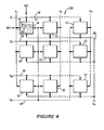
- FIGURE 4 there is shown a memory array 58 comprising a plurality of nonvolatile memory cells constructed as described hereinabove with reference to memory cell 10.
- Third substrate region 36 is a bulk implant region common to each cell 10 as best seen in FIGURE 4.
- First semiconductor layer 14, to which the bias potential is applied, is also common to each cell 10 and may be a bulk semiconductor layer.
- Each third semiconductor layer 18, in the preferred embodiment of the present invention, forms a word line Yi common to a row of nonvolatile memory cells 10.
- first word line Y 1 connects the top row 60 of nonvolatile memory cells 10 in memory array 50.
- word line Y 1 is a bulk semiconductor layer forming third layer 18 of each nonvolatile cell 10 in row 60.
- First substrate region 20 in each column of nonvolatile memory cell 10 is connected to a bit line X j .
- the bit line X 1 is coupled to the first substrate region 20 of each cell.
- Each substrate region 20 in column 62 is connected to bit line X 1 by a metallization deposited over oxide.
- the above described array 58 when configured as an EEPROM device, has several advantages compared to the EEPROM device disclosed in U. S. Patent No. 4,486,769 in terms of eliminating data disturb problems in unselected memory cells.
- One such advantage is the elimination of partial tunneling voltages appearing across either of tunneling element 28 or tunneling element 34 in any unselected cell. Since transistor 38 is operated in a cutoff condition in all unselected cells, no partial voltage can be coupled to the floating gate 16 in such unselected cell by the application of a high data potential V D along any column data line Xj to the first substrate region 20 of the unselected cell.
- the device of array 58 selects all cells along a row having a common word line Yi formed by third polysilicon layer 18. This word select capability of array 58 eliminates the application of a high voltage to one side of a tunneling element in an unselected cell.
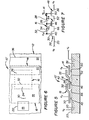
- FIGURES 5-7 there is shown an alternate embodiment of a nonvolatile memory cell 10' which allows further miniaturization over the above-described nonvolatile memory cell 10.
- Identical reference numerals are used in FIGURES 5-7 to identify the identical components described above in conjunction with nonvolatile memory cell 10 with reference to FIGURES 1-3.
- the difference in fabrication in nonvolatile memory cell 10' is the elimination of second substrate region 22 underneath floating gate 16 and hence the elimination of capacitor C s .
- the elimination of this capacitance allows the dimensions of floating gate 16 to be reduced since it does not need to function as one plate of capacitor C s .
- second substrate region 22 elimination of second substrate region 22 allows second semiconductor layer 16 and third semiconductor layer 18 to be made smaller so that the critical dimensions, especially overlap, are selected with regard only to the capacitive coupling therebetween to form tunneling region 34.
- the other remaining construct on the size of second semiconductor layer 16 is that its overlap to first semiconductor layer 14 must be sufficient to achieve the necessary capacitive coupling to form first tunneling region 28.
- nonvolatile memory cell 10' instead of having second substrate region 22 form a conduction path between transistors 38 and 44, a virtual junction 66 is formed therebetween, connecting the channel region 40 of transistor 38 and the channel region 46 of transistor 44.
- transistor 44 and transistor 48 are equivalent to a triple gate enhancement mode transistor.
- the construction of nonvolatile memory cell 10' is identical to the above-described nonvolatile memory cell 10.
- nonvolatile memory cell 10' may be used in the memory array described with reference to FIGURE 4.
- a further advantage to removing second substrate region 22 is the reduction in the size of memory cell 10' by virtue of the removal of the substrate region separation requirements imposed by alignment tolerances, critical dimension control or electrical constraints.
- the size of second substrate region 22 and first portion 24 of floating gate 16 are determined by alignment and electrical requirements required to ensure a properly sized channel 46 of floating gate transistor 44 and sufficiently sized plates for capacitor C s , as well as ensuring channel 40 is of proper length for transistor 38.
- the overlap requirements of third polysilicon layer 18 to second substrate region 22 also must be considered in sizing region 22. Without any overlap, discontinuity may occur between channel 40 of transistor 38 and second substrate region 22. In nonvolatile memory cell 10', this overlap requirement is eliminated, thereby eliminating these tolerance constraints between mask layers.
- the tunneling region can be thought of as a voltage actuated switch having zero conduction for a voltage less than V x and a very high conduction for a voltage greater than or equal to V x .
- the bias potential V R is set to zero volts.
- V x 12 volts and V H equals 20 volts and C e equals Cp while C s is approximately equal to 3 C e
- V f g after programming is approximately -4 volts.
- the operation of the memory cell, and the final programming voltage level of the floating gate changes as follows.
- the channel region 40 of transistor 38 in nonvolatile memory cell 10' can at most support a surface potential which is equivalent to V f g-V t where V t is the threshold voltage of transistor 38. Beyond this value, the channel is fully depleted and its capacitance contribution virtually disappears. Therefore, the floating gate voltage after programming from the above equation would be aDDroximated bv where again Cp is the capacitance of tunneling element 28 and C e is the capacitance of tunneling element 34.
- the floating gate voltage after programming works out to +2 volts, or the loss of 6 volts in programming margin as compared to nonvolatile memory cell 10.
- nonvolatile memory cell 10 When erasing the floating gate, i.e. tunneling electrons from floating gate 16 to third polysilicon layer 18, there is little functional difference between the embodiments of nonvolatile memory cell 10 and that of memory cell 10'. Erasing occurs when first substrate region 20 is maintained at zero volts by the data potential V D . In cell 10', the surface potential of channel 46 under full inversion, i.e. where the substrate changes conductivity, provides the same function as the potential of second substrate region 22 in nonvolatile memory cell 10.
- the state of the floating gate 16 is sensed by applying a potential to first semiconductor layer 14 sufficient to invert the conductivity type of channel 50, so that the potential of third substrate region 36 is coupled to channel 46.
- Another potential is applied to third semiconductor layer 18 along control potential line V B also sufficient to invert the conductivity type of channel 40 to couple either of second substrate region 22 of nonvolatile memory cell 10 or virtual junction 66 of nonvolatile memory cell 10' to first substrate region 20.
- the sense potential will develop a sense current of value dependent on the conduction of transistor 44 at each data node, which represents one binary state. If the floating gate is sufficiently programmed, i.e.
- the conductivity type of channel 46 will not be inverted, therefore leaving transistor 44 off, whereby no current is enabled between first substrate region 20 and third substrate region 36.
- floating gate 16 is erased, i.e. it contains a positive potential, conductivity of channel 46 will be inverted, thereby turning transistor 44 on, whereby a current will be developed between first substrate region 20 and third substrate region 36.
- the state of the sense current represents the two binary states, programmed and erased, respectively.
- a third approach is to lessen the potential difference between each of V E , V R and V D to V G .
- the read voltage magnitude of V H may be lowered or alternatively the potential V G may be raised.
- equation (2) decreasing of Cp relative to C e sufficiently will make V f g go more negative, resulting in full cutoff. It is within the ordinary skill of the art to provide such sense means in a memory array.
- Each semiconductor layer 14, 16 and 18 may be constructed by selectively etching deposited polysilicon. It will be appreciated that other variations and modifications to the present invention may be made without departing from the inventive concepts described herein. Accordingly, the present invention is to be limited solely by the scope of the appended claims.
Landscapes
- Engineering & Computer Science (AREA)
- Microelectronics & Electronic Packaging (AREA)
- Non-Volatile Memory (AREA)
- Read Only Memory (AREA)
Abstract
Description
- The present invention relates generally to integrated circuit programmable nonvolatile memory devices, and more particularly to an improved nonvolatile memory cell for increasing the density of the nonvolatile memory cells in such memory devices.
- In the prior art, integrated circuit memory devices have been developed which store data for indefinite periods of time in the absence of electrical power being applied thereto and which also have the capability of selectively changing or programming the data stored therein. Of particular interest herein is a nonvolatile memory cell which utilizes a floating gate as the nonvolatile element. See e.g., U.S. Patent No. 4,314,265 which discloses a four polysilicon layer, floating gate nonvolatile memory cell, and U.S. Patent No. 4,274,012 which discloses a three polysilicon layer, floating gate nonvolatile memory cell with substrate coupling. Either of these nonvolatile memory cells may be arranged, as is known in the art, to construct nonvolatile random access memories (NOVRAM's) and electrically erasable programmable read only memories (EEPROM's). See, e.g., U.S. Patent No. 4,300,212, which discloses a NOVRAM device and U.S. Patent No. 4,486,769, which discloses an EEPROM device. Of course, the principles of the present invention are applicable to other devices utilizing floating gate technology.
- In U.S. Patent No. 4,274,012, for example, the disclosed nonvolatile memory cell has three layers of polysilicon, each layer being generally electrically isolated from the substrate and each other. The first polysilicon layer is a programming electrode. The second polysilicon layer is the floating gate. The floating gate has a portion capacitively coupled to the programming electrode to form a programming tunneling region in which electrons tunnel from the programming electrode to the floating gate. Another portion of the floating gate is capacitively coupled to a n-implant region in the p-type substrate. The n-implant region is a bias electrode. The third polysilicon layer, which is an erase/store electrode, is capacitively coupled to a portion of the floating gate to form an erase tunneling region in which electrons tunnel from the floating gate to the erase/store electrode. Another portion of the erase/store electrode is capacitively coupled to the bias electrode in the substrate.
- To initiate tunneling, a high potential, such as 25v, is applied to the erase/store electrode while the programming electrode is held at a low potential, such as ground. The substrate bias electrode is caused to be held either at the low potential of the programming electrode or held at the high potential of the erase/store electrode, depending on whether electrons are to be tunneled from or to the floating gate, respectively. With the bias electrode held at the high potential, the floating gate being strongly capacitively coupled to the bias electrode is elevated to the high potential. Therefore, high potential exists across the programming tunneling region between the programming electrode and the floating gate so that electrons are tunneled onto the floating gate. Conversely, with the bias electrode held at the low potential, the floating gate will also be at the low potential because of the strong capacitive coupling to the bias electrode. Therefore, high potential exists across the erase tunneling region between the floating gate and the erase/store electrode. Electrons will then tunnel from the floating gate to the erase/store electrode.
- The above-described nonvolatile memory cell, in one useful application, forms the nonvolatile portion of a NOVRAM memory cell disclosed in U.S. Patent No. 4,300,212. The volatile portion of the NOVRAM memory cell is addressed, read from and written to in a manner known for MOS flip-flop type memory cells. The nonvolatile portion of the NOVRAM memory cell is coupled to the data and inverse data nodes of the volatile portion of the NOVRAM memory cell. The bias electrode is connected to the drain of an enhancement mode transistor with a grounded source. The data node of the volatile portion of the NOVRAM memory cell is coupled to the gate of this transistor. When the data node is at zero volts, representing one binary state, the transistor is turned off allowing the bias electrode to be at a floating potential. The bias electrode is further capacitively coupled to the erase/store electrode. Application of the high voltage store pulse to the erase/store electrode will cause the potential of the bias electrode to be elevated to the high potential. Electrons will then tunnel from the programming electrode to the floating gate, as described hereinabove, giving it a net negative charge. Conversely, when the data node is at 5 volts, representing the other binary state, the transistor is turned on thereby coupling the bias electrode to zero volts. Application of the high voltage pulse to the erase/store electrode will cause electrons to be removed from the floating gate by tunneling to the erase/store electrode, as described hereinabove, leaving a net positive charge thereon. Therefore, the charge of the floating gate stores the state of the data node of the volatile portion of the NOVRAM cell when the high voltage pulse is applied to the erase/store electrode.
- To sense the charge on the floating gate, the floating gate forms the gate of an enhancement mode sense transistor. The drain of the sense transistor is coupled to the inverse data node of the volatile portion of the NOVRAM memory cell. The sense transistor is turned on when the floating gate has a net positive charge and is turned off when the floating gate has a net negative charge. Thus, the charge stored on the floating gate may be determined from the on or off state of the sense transistor and the potential of the inverse data node set therefrom upon power up of the NOVRAM device.
- The nonvolatile memory cell described in U.S. Patent No. 4,274,012, in another useful application, is used in the construction of each memory cell in an array of cells of an EEPROM device as disclosed in U.S. Patent No. 4,486,769. In the array disclosed in this patent, the erase/store electrode is common to each cell in a column, and the programming electrode is common to each cell in a row. Furthermore, the bias electrode in each cell along a row are electrically connected to each other. To select one cell in the array, the programming electrode across the row in which the selected cell is located is held to a low potential, such as 0 volts and the erase/store electrode of the column in which the selected cell is located is raised to a high potential, such as 36 volts. The programming electrode in all other rows.is raised to an intermediate potential, such as 26 volts and the erase/store electrode in all other columns is held to a low potential, such as 0 volts. The bias electrode for each cell in the row of the selected cell is driven to either the intermediate potential or the low potential, depending on whether the floating gate of the selected cell is to be programmed or erased, respectively. The bias electrode for cells in all other rows is driven to the intermediate potential. As described in the '769 patent, the full potential difference between the low and high potentials will exist across either the programming tunneling element or the erase tunneling element in the selected cell as a function of the bias electrode potential. Electrons will then tunnel across the selected tunneling element.
- In all other cells along the row of the selected cell in this prior art EEPROM device, a potential difference exists across the tunneling element between its programming electrode and floating gate. The intermediate voltage applied to the bias electrode of the unselected cell is partially coupled to the floating gate while the programming electrode is held at the low potential. Since the unselected cell's erase/store electrode is also held to zero volts, the capacitive coupling between the erase/store electrode and the floating gate prevents the floating gate from having the same voltage as the bias electrode. Thus, when the capacitive relationships are selected as describe in the '769 patent, the floating gate in each of the cells in the row of the selected cell will not have a potential sufficient to initiate tunneling of electrons to the floating gate.
- Similarly, a potential difference will exist across the tunneling region between the erase/store electrode and floating gate of all other cells in the column of the selected cell. Since-the bias electrode and programming electrode of all nonselected cells in this column are at the intermediate potential, their floating gates will also have a potential near the intermediate potential. The erase/store electrode of these selected cells in the column will be at the high potential. The resultant potential difference across the erase tunneling region is therefore insufficient to cause elections to tunnel from the floating gate.
- In each cell of this EEPROM device, a pair of transistors are coupled to the channel region of the substrate adjacent the floating gate. The gate of each of these transistors is formed from the erase/store electrode. Data potential is coupled to the channel region through one transistor and bias electrode potential is coupled to the channel region through the other transistor. To erase the floating gate, both the data potential and the bias electrode potential are at the low potential. To program the floating gate, both the data potential and the bias electrode potential are at the intermediate potential.
- The above approach has several limitations. First, a number of capacitance interrelationships and tunnel voltage requirements must be maintained in order to avoid data disturbs of unselected cells during a write operation. In addition, logistical requirements of arrayed cells can make a single cycle write operation difficult to implement in practice. Consequently, in practical operation, before the floating gate is programmed, each EEPROM cell is first erased. Thus, each write cycle to a memory cell is preceded by an unconditional erase cycle, incurring unnecessary write time and cell wear out.
- It is desirable to increase the number of memory devices which are fabricated from a single wafer to increase the chip yield per wafer and thereby to reduce the cost of.each chip. In this regard, the size of each memory cell within the memory device must be reduced. However, such reductions in size do not allow a simple miniaturization of existing memory cells. For example, tolerances between mask levels may be difficult to maintain or the miniaturized design may require minimum channel widths not compatible with existing technology. Miniaturization of the above-described nonvolatile memory cell does not allow the necessary capacitive values and relationships to be maintained for an operational memory device. For example, should the required capacitive relationships in the EEPROM device described in the '769 patent not be maintained, the voltages described as occurring across the tunneling regions of unselected cells in the row and columns of the selected cell may be sufficient to cause inadvertent tunneling or a data disturb of the unselected cell. Furthermore, the overhead requirements of a separate and distinct bias electrode region for a write operation, and floating gate channel region for a read operation, combined with the aforementioned inherent tolerance requirements needed to prevent disturb conditions, makes shrinking of present memory cells for very high density applications impractical.
- It is also desirable to eliminate one or more of the above-described capacitive couplings in the NOVRAM device. Such capacitive couplings introduce losses in obtaining the voltage relationships necessary to induce tunneling of electrons between the polysilicon layers. Eliminating such capacitors, therefore, would improve device operation. Furthermore, the elimination of these capacitances enables a greater degree of miniaturization, since the need for the large amount of chip real estate required to form such capacitors would be eliminated.
- Furthermore, device operation and cell dimensions could be optimized by reducing component count in each memory cell and reducing the number of cycles required for a write operation. For example, in the EEPROM device, it is desirable that a write cycle (programming the floating gate) be accomplished in a single cycle obviating the need for an unconditional erase prior to each write cycle.
- It is therefore an object of the present invention to provide a nonvolatile memory cell which is smaller than known nonvolatile memory cells.
- It is an important object of the present invention to provide a nonvolatile memory cell which utilizes fewer components than known memory cells.
- It is a further object of the present invention to provide a nonvolatile memory cell which eliminates some capacitive relationships, thereby minimizing the chip real estate required for forming such cells, since less overlap between layers of the memory cell is required.
- It is another object of the present invention to provide a nonvolatile memory cell which obviates the requirement of an unconditional erase cycle prior to programming the floating gate.
- It is yet a further object of the present invention to provide a dense nonvolatile integrated circuit memory device which substantially eliminates data disturb conditions in unselected cells of the memory device when writing into one or more selected cells.
- The nonvolatile memory cell of the present invention includes three electrically isolated semiconductor layers, generally as described hereinabove. That is, the first layer forms the programming electrode, the second layer forms the floating gate, and the third layer forms the erase/store electrode.
- According to the present invention, a first portion of the second layer is capacitively coupled to the first layer to form a first tunneling region therebetween, and a second portion of the second layer is capacitively coupled to a substrate region of opposite conductivity to the substrate. A third semiconductor layer is capacitively coupled to the second layer to form a second tunneling region. In operation, a reference potential is applied to the first layer. A voltage representative of the data state to be stored by the charge on the second layer is applied to another substrate region of opposite conductivity to the substrate type. The third layer forms the gate of an enhancement mode transistor between each substrate region. Upon application of a selected potential to the third layer, the transistor is turned on to create a conductive path between each substrate region. If the data state voltage is similar to the potential applied to the third layer, electrons will tunnel from the first layer to the second layer leaving the second layer with a net negative charge. Conversely, if the data state voltage is significantly less than the voltage of the potential applied to the third layer, electrons will tunnel from the second layer to the third layer leaving the second layer with a net positive charge.
- Thus, an advantage of the present invention over the above-described prior art devices is seen. The present invention eliminates the need for capacitive coupling between the third semiconductor layer, the erase/store electrode, and the bias electrode as described above with reference to the NOVRAM device. As previously described, the capacitive coupling allowed the bias electrode to float to the potential of the erase/store electrode. The transistor switch needed to control the potential of the bias electrode in the nonvolatile cell of the NOVRAM device is also eliminated.
- In the present invention, the potential of the substrate region capacitively coupled to the second layer, the region that is analogous to the bias electrode described in the prior art, is determined by the data state potential. The third layer forms the transistor gate which controls conductivity between the first and second substrate regions, thereby eliminating the need for a separate transistor switch for controlling the bias electrode potential.
- Furthermore, the substrate region of opposite conductivity to the substrate and capacitively coupled to the second layer may be eliminated altogether. In a second embodiment of the present invention, the capacitive relationships required to induce tunneling between the first and second layer or second and third layer are controlled by the capacitance inherent between the second layer and the substrate itself. By eliminating the first substrate region altogether, the nonvolatile cell may have overall dimensions considerably less than the prior art nonvolatile cells described hereinabove, since the overlap dimensions of the layers which form such capacitances are eliminated. A further advantage of the second embodiment of the present invention is that it requires one less semiconductor layer as compared with the memory cell disclosed in Patent No. 4,314,265, a prior art cell also having no substrate electrode.
- These and other objects and advantages of the present invention will become more apparent from the following specification when read in conjunction with the accompanying drawings and appended claims.
-
- FIGURE 1 is a schematic cross sectional view - of a nonvolatile memory cell constructed according to the present invention;
- FIGURE 2 is a plan view of the memory cell of FIGURE 1;
- FIGURE 3 is an equivalent electrical circuit of the nonvolatile memory cell illustrated in FIGURE 1;
- FIGURE 4 is an equivalent electrical schematic block diagram of an array of memory cells, constructed according to the principles of the present invention useful for illustrating formation of an integrated circuit nonvolatile memory device according to the present invention;
- FIGURE 5 is a schematic cross sectional view of another embodiment of a nonvolatile memory cell according to the present invention;
- FIGURE 6 is a plan view of the memory cell of FIGURE 5; and
- FIGURE 7 is an equivalent electrical circuit of the memory cell of FIGURE 5.
- Referring now to FIGURES 1-3, there is shown a
nonvolatile memory cell 10 constructed according to the present invention.Memory cell 10 includes asubstrate 12 of a first conductivity type, a first electrically isolatedsemiconductor layer 14, a second electrically isolatedsemiconductor layer 16 and a third electricallyisolated semiconductor layer 18. -
Substrate 12 includes afirst substrate region 20, asecond substrate region 22, and asurface 23. Eachsubstrate region surface 23 and is of a second conductivity type opposite the first conductivity type ofsubstrate 12. -
Second semiconductor layer 16 has afirst portion 24 capacitively coupled tosecond substrate region 22 and asecond portion 26 capacitively coupled tofirst semiconductor layer 14. The capacitive coupling betweenfirst portion 24 ofsecond layer 16 andsecond substrate region 22 is best seen in FIGURE 3 as capacitance Cs. The capacitive coupling betweensecond portion 26 ofsecond layer 16 andfirst layer 14 is best seen in FIGURE 3 as atunneling region 28. -
Third semiconductor layer 18 has afirst portion 30 extending betweenfirst substrate region 20 andsecond substrate region 22 and spaced fromsurface 23, and asecond portion 32 capacitively coupled tosecond layer 16. The capacitive coupling ofsecond portion 32 tosecond layer 16 is best seen in FIGURE 3 as atunneling region 34. -
Substrate 12 further includes athird substrate region 36 of the second conductivity type.First semiconductor layer 14 andthird substrate region 36 extend generally parallel with each other.First semiconductor layer 14 andthird substrate region 36 are common to eachcell 10 of the memory array described hereinbelow. The parallel relationship between these elements simplifies the fabrication process and operation of the array as well as satisfying the electrical relationships betweenfirst semiconductor layer 14 andthird substrate region 36, as described herein. - As best seen in FIGURE 3,
first portion 30 ofthird semiconductor layer 18 forms the gate of anenhancement mode transistor 38, having achannel 40 disposed betweenfirst substrate region 20 andsecond substrate region 22. Theselatter substrate regions transistor 38, respectively. Athird portion 42 ofsecond semiconductor layer 16 forms the gate of aninsulated gate transistor 44, also referred to herein as the floating gate transistor.Transistor 44 is an enhancement mode transistor in the present embodiment but could also be a depletion mode as well if performance adjustments are needed.Second substrate region 22 forms the drain oftransistor 44.Third portion 42 ofsecond semiconductor layer 16 overlays achannel 46 oftransistor 44.First semiconductor layer 14 forms the gate of aenhancement mode transistor 48.Transistor 48 could also be a depletion mode transistor as well if performance adjustments are needed.Third substrate region 36 forms the source oftransistor 48.First semiconductor layer 14 overlies achannel 50 oftransistor 48.Transistors region 52 betweenchannel 46 andchannel 50 oftransistor 44 andtransistor 48, respectively.Region 52 can be best described as a virtual junction.Transistor 44 andtransistor 48 are equivalent to a single enhancement (or depletion, if so used) mode transistor having two adjacent gates, whereinthird portion 42 ofsecond semiconductor layer 16 forms one gate andfirst semiconductor layer 14 forms a second gate adjacent the first gate thereof. - Having described above the construction of
nonvolatile memory cell 10, described below the operation of thisnonvolatile memory cell 10. The mechanism for tunneling of electrons acrosstunneling regions cell 10 to electrically isolate it from the next level of semiconductor material deposited on the device. The requirements for the thickness of the oxide layers between the semiconductor layers 14, 16 and 18 are described in the '012 patent. Therefore, the portions of the '012 patent which describe the tunneling of electrons through the oxide layer, as well as the requirements for the thickness of the oxide separating the semiconductor layers and the capacitive relationships necessary to enable tunneling and which are not inconsistent with the disclosure of the present invention, are incorporated herein by reference. - A bias potential VR is applied to
first semiconductor layer 14 and a reference potential VG is applied tothird substrate region 36. For high voltage power considerations during tunneling of electrons across eithertunneling region 28 ortunneling region 34, the bias potential offirst semiconductor layer 14 forming the gate oftransistor 48 and the reference potential ofthird substrate region 36 forming the source oftransistor 48 are selected so that no current is developed inchannel 50 from virtual junction 52 (equivalent to the electrical connection between the drain oftransistor 48 and source of transistor 44) tothird substrate region 36 in either direction. Accordingly, the gate-source voltage, given by VR-VG, oftransistor 48 is normally biased negatively in a preferred embodiment of the present invention during tunneling so thattransistor 48 remains in a "cutoff" condition irrespective of the drain voltage atvirtual junction 52. - A data potential VD is applied to
first substrate region 20 whose level represents the data state to be stored onsecond semiconductor layer 16. For example, the first binary state may be represented by a low potential and the other binary state may be represented by a high potential. Concurrently with applying the data potential VD tofirst substrate region 20, a control potential VH is applied tothird semiconductor layer 18. The control potential Vg is selected to invert the conductivity ofchannel 40 sufficiently to conduct the full data potential VD applied tofirst substrate region 20 tosecond substrate region 22 through turned ontransistor 38. The control potential Vg and the data potential VD, when VD is in a high data potential state, are selected to ensure that sufficient potential difference exists across thetunneling region 28 so that electrons tunnel tosecond semiconductor layer 16. With control potential VH set at the level just described, the data potential VD, when VD is in a low data potential state, is selected so that sufficient potential difference exists across tunnelingregion 34 so that electrons may tunnel fromsecond semiconductor layer 16 tothird semiconductor layer 18.Second semiconductor layer 16 forms the floating gate ofnonvolatile memory cell 10 and is hereinafter also referred to as floatinggate 16. - For example, when the data potential VD applied to
first substrate region 20 is high and a sufficiently high control potential VH is applied tothird semiconductor layer 18, the data potential VD is coupled tosecond substrate region 22, causingsubstrate 22 to also attain a high potential so that little potential difference exists betweenthird semiconductor layer 18 andsecond substrate region 22. Floatinggate 16 will also attempt to reach a high potential because of the capacitive coupling of capacitor Cs and the capacitive effects oftunneling element 34 andchannel 46. As the potential of floatinggate 16 goes high, little potential difference will exist across tunnelingregion 34 and a large potential difference will then exist across tunnelingregion 28. Consequently, electrons will tunnel fromfirst semiconductor layer 14 to floatinggate 16. - Conversely, when the data voltage Vp is low, the potential of
second substrate region 22 is also low. The capacitance Cs betweenfirst portion 24 of floatinggate 16 andsecond substrate region 22 as well as the capacitive effects oftunneling element 28 andchannel region 46 will attempt to capacitively hold the floatinggate 16 low upon application of the control potential VH tothird semiconductor layer 18. Therefore, the potential difference across tunnelingregion 28 is small and the potential difference across tunnelingregion 34 is large. As a result, electrons will tunnel from floatinggate 16 tothird semiconductor layer 18. - An advantage of the present invention over the memory cells disclosed in the above-identified patents is that the n-implant regions of the
first substrate region 20 andsecond substrate region 22 may be considerably smaller than the bias electrode shown in these patents. In contrast to the NOVRAM device described in the '212 patent, no capacitive coupling is required between thethird semiconductor layer 18 and a bias electrode in the substrate. In the NOVRAM device, it was this capacitive coupling which let the bias electrode float to the potential of the control voltage to bias the floating gate. Since such capacitive coupling is not required in the present invention, the third semiconductor layer may be made smaller since no dimensions necessary for the capacitive tolerances need be maintained. Described below is the advantage of the present invention over the prior art in terms of eliminating data disturb problems in EEPROM memory cells that are not being written to. - In digital systems, binary state voltage levels are usually 0 volts and +5 volts. It is desirable that the integrated circuit memory device utilizing
nonvolatile memory cell 10 of the present invention is operable from these voltages. A charge pump may be included in the integrated circuit memory device to obtain a high potential in the range 25-35 volts from an externally applied 5 volt source. Such a charge pump is described in U.S. Patent No. 4,326,134. The portions of this patent describing the control of the charge pump and switching of the high potential to the nonvolatile memory cell are incorporated herein by reference. Of course, it is within the ordinary skill of the art to provide a data voltage Vp substantially equal to control voltage VB when the incoming binary data has one data state and to provide a VD of zero volts when the incoming binary data has the other binary state. - The
nonvolatile memory cell 10 in accordance with the invention can be used to form a memory array such as an electrically alterable read only memory array with the addition of commonly known decoding and buffering systems in such memory devices. - Referring now to FIGURE 4, there is shown a
memory array 58 comprising a plurality of nonvolatile memory cells constructed as described hereinabove with reference tomemory cell 10.Third substrate region 36 is a bulk implant region common to eachcell 10 as best seen in FIGURE 4.First semiconductor layer 14, to which the bias potential is applied, is also common to eachcell 10 and may be a bulk semiconductor layer. Eachthird semiconductor layer 18, in the preferred embodiment of the present invention, forms a word line Yi common to a row ofnonvolatile memory cells 10. For example, first word line Y1 connects thetop row 60 ofnonvolatile memory cells 10 inmemory array 50. Thus, word line Y1 is a bulk semiconductor layer formingthird layer 18 of eachnonvolatile cell 10 inrow 60.First substrate region 20 in each column ofnonvolatile memory cell 10 is connected to a bit line Xj. For example, in thefirst column 62 ofnonvolatile memory cells 10, the bit line X1 is coupled to thefirst substrate region 20 of each cell. Eachsubstrate region 20 incolumn 62 is connected to bit line X1 by a metallization deposited over oxide. Of course, it is within the ordinary skill of the art to provide row and column decoders in a memory array. - The above described
array 58, when configured as an EEPROM device, has several advantages compared to the EEPROM device disclosed in U. S. Patent No. 4,486,769 in terms of eliminating data disturb problems in unselected memory cells. One such advantage is the elimination of partial tunneling voltages appearing across either oftunneling element 28 ortunneling element 34 in any unselected cell. Sincetransistor 38 is operated in a cutoff condition in all unselected cells, no partial voltage can be coupled to the floatinggate 16 in such unselected cell by the application of a high data potential VD along any column data line Xj to thefirst substrate region 20 of the unselected cell. Furthermore, in contrast to the selection of a single cell, as described in the '769 patent, the device ofarray 58 selects all cells along a row having a common word line Yi formed bythird polysilicon layer 18. This word select capability ofarray 58 eliminates the application of a high voltage to one side of a tunneling element in an unselected cell. - Referring now to FIGURES 5-7, there is shown an alternate embodiment of a nonvolatile memory cell 10' which allows further miniaturization over the above-described
nonvolatile memory cell 10. Identical reference numerals are used in FIGURES 5-7 to identify the identical components described above in conjunction withnonvolatile memory cell 10 with reference to FIGURES 1-3. The difference in fabrication in nonvolatile memory cell 10' is the elimination ofsecond substrate region 22 underneath floatinggate 16 and hence the elimination of capacitor Cs. The elimination of this capacitance allows the dimensions of floatinggate 16 to be reduced since it does not need to function as one plate of capacitor Cs. Also, elimination ofsecond substrate region 22 allowssecond semiconductor layer 16 andthird semiconductor layer 18 to be made smaller so that the critical dimensions, especially overlap, are selected with regard only to the capacitive coupling therebetween to formtunneling region 34. The other remaining construct on the size ofsecond semiconductor layer 16 is that its overlap tofirst semiconductor layer 14 must be sufficient to achieve the necessary capacitive coupling to formfirst tunneling region 28. - Further according to alternate embodiment 10', instead of having
second substrate region 22 form a conduction path betweentransistors virtual junction 66 is formed therebetween, connecting thechannel region 40 oftransistor 38 and thechannel region 46 oftransistor 44. Thus, in the circuit of FIGURE 7transistor 44 andtransistor 48 are equivalent to a triple gate enhancement mode transistor. Otherwise, the construction of nonvolatile memory cell 10' is identical to the above-describednonvolatile memory cell 10. Furthermore, nonvolatile memory cell 10' may be used in the memory array described with reference to FIGURE 4. - A further advantage to removing
second substrate region 22 is the reduction in the size of memory cell 10' by virtue of the removal of the substrate region separation requirements imposed by alignment tolerances, critical dimension control or electrical constraints. For example, the size ofsecond substrate region 22 andfirst portion 24 of floatinggate 16 are determined by alignment and electrical requirements required to ensure a properlysized channel 46 of floatinggate transistor 44 and sufficiently sized plates for capacitor Cs, as well as ensuringchannel 40 is of proper length fortransistor 38. The overlap requirements ofthird polysilicon layer 18 tosecond substrate region 22 also must be considered in sizingregion 22. Without any overlap, discontinuity may occur betweenchannel 40 oftransistor 38 andsecond substrate region 22. In nonvolatile memory cell 10', this overlap requirement is eliminated, thereby eliminating these tolerance constraints between mask layers. - Referring now in greater detail to the operational characteristics of
nonvolatile memory cell 10 of FIGURES 1-3, the tunneling region can be thought of as a voltage actuated switch having zero conduction for a voltage less than Vx and a very high conduction for a voltage greater than or equal to Vx. In the following example, the bias potential VR is set to zero volts. When the control potential Va is less then twice the potential Vx and the data potential VD is equal to the control potential Vg, then during programming of floatinggate 16 when Vfg of floatinggate 16 attempts to go beyond the potential VX, the potential Vfg of floatinggate 16 becomes clamped to Vx resulting in a floating gate potential after programming given approximately by the equation
tunneling element 28 and Ce is the capacitance oftunneling element 34. - For example, if Vx equals 12 volts and VH equals 20 volts and Ce equals Cp while Cs is approximately equal to 3 Ce, the floating gate potential Vfg after programming is approximately -4 volts.
- By removing
substrate region 22, and hence capacitor Cs, and having its function provided bychannel 46 of floatinggate transistor 44, as illustrated in the nonvolatile memory cell 10' of FIGURE 5, the operation of the memory cell, and the final programming voltage level of the floating gate, changes as follows. Unlikesubstrate region 22, which can support the full high voltage of VD, thechannel region 40 oftransistor 38 in nonvolatile memory cell 10' can at most support a surface potential which is equivalent to Vfg-Vt where Vt is the threshold voltage oftransistor 38. Beyond this value, the channel is fully depleted and its capacitance contribution virtually disappears. Therefore, the floating gate voltage after programming from the above equation would be aDDroximated bv
tunneling element 28 and Ce is the capacitance oftunneling element 34. - Using the same voltage levels given above by example, the floating gate voltage after programming works out to +2 volts, or the loss of 6 volts in programming margin as compared to
nonvolatile memory cell 10. - When erasing the floating gate, i.e. tunneling electrons from floating
gate 16 tothird polysilicon layer 18, there is little functional difference between the embodiments ofnonvolatile memory cell 10 and that of memory cell 10'. Erasing occurs whenfirst substrate region 20 is maintained at zero volts by the data potential VD. In cell 10', the surface potential ofchannel 46 under full inversion, i.e. where the substrate changes conductivity, provides the same function as the potential ofsecond substrate region 22 innonvolatile memory cell 10. - In either
nonvolatile memory cell 10 or nonvolatile memory cell 10', the state of the floatinggate 16 is sensed by applying a potential tofirst semiconductor layer 14 sufficient to invert the conductivity type ofchannel 50, so that the potential ofthird substrate region 36 is coupled tochannel 46. Another potential is applied tothird semiconductor layer 18 along control potential line VB also sufficient to invert the conductivity type ofchannel 40 to couple either ofsecond substrate region 22 ofnonvolatile memory cell 10 orvirtual junction 66 of nonvolatile memory cell 10' tofirst substrate region 20. By applying a sense potential to data nodes represented byfirst substrate region 20, the sense potential will develop a sense current of value dependent on the conduction oftransistor 44 at each data node, which represents one binary state. If the floating gate is sufficiently programmed, i.e. with enough negative potential, the conductivity type ofchannel 46 will not be inverted, therefore leavingtransistor 44 off, whereby no current is enabled betweenfirst substrate region 20 andthird substrate region 36. However, if floatinggate 16 is erased, i.e. it contains a positive potential, conductivity ofchannel 46 will be inverted, thereby turningtransistor 44 on, whereby a current will be developed betweenfirst substrate region 20 andthird substrate region 36. The state of the sense current represents the two binary states, programmed and erased, respectively. - In the case of memory cell 10', since the cutoff characteristics of floating
gate transistor 44 are not as well established as that of floatinggate transistor 44 innonvolatile memory cell 10 for the programmed state of floatinggate 16, a number of strategies may be employed to reliably sense this state. One approach would be to discriminate between the higher conduction level of the erased state and the lower conduction level of the programmed state, using an intermediate reference current combined with conventional differential sensing. A second approach would be to adjust the threshold of floatinggate transistor 44 upward thereby retarding the turn-on characteristics of this transistor so that the floatinggate transistor 44 is cut off when floatinggate 16 is in the programmed state with a less positive potential as compared to the erased state. A third approach is to lessen the potential difference between each of VE, VR and VD to VG. For example, the read voltage magnitude of VH may be lowered or alternatively the potential VG may be raised. Yet another approach is suggested by equation (2) decreasing of Cp relative to Ce sufficiently will make Vfg go more negative, resulting in full cutoff. It is within the ordinary skill of the art to provide such sense means in a memory array. - The present invention has been described utilizing n-channel technology. It is within the ordinary skill of the art to use p-channel technology. In this regard, the potential described above would be opposite in polarity. Each
semiconductor layer
Claims (29)
Applications Claiming Priority (2)
| Application Number | Priority Date | Filing Date | Title |
|---|---|---|---|
| US06/734,478 US4599706A (en) | 1985-05-14 | 1985-05-14 | Nonvolatile electrically alterable memory |
| US734478 | 1991-07-23 |
Publications (3)
| Publication Number | Publication Date |
|---|---|
| EP0202785A2 true EP0202785A2 (en) | 1986-11-26 |
| EP0202785A3 EP0202785A3 (en) | 1990-05-30 |
| EP0202785B1 EP0202785B1 (en) | 1992-03-18 |
Family
ID=24951858
Family Applications (1)
| Application Number | Title | Priority Date | Filing Date |
|---|---|---|---|
| EP86303076A Expired EP0202785B1 (en) | 1985-05-14 | 1986-04-23 | Nonvolatile electrically alterable memory |
Country Status (4)
| Country | Link |
|---|---|
| US (1) | US4599706A (en) |
| EP (1) | EP0202785B1 (en) |
| JP (1) | JPS61265869A (en) |
| DE (1) | DE3684359D1 (en) |
Cited By (4)
| Publication number | Priority date | Publication date | Assignee | Title |
|---|---|---|---|---|
| EP0295935A1 (en) * | 1987-06-19 | 1988-12-21 | Advanced Micro Devices, Inc. | Electrically erasable programmable read only memory |
| EP0280883A3 (en) * | 1987-01-31 | 1989-02-08 | Kabushiki Kaisha Toshiba | Nonvolatile semiconductor memory |
| EP0284724A3 (en) * | 1987-01-31 | 1989-03-08 | Kabushiki Kaisha Toshiba | Nonvolatile semiconductor memory device |
| WO1990011621A1 (en) * | 1989-03-27 | 1990-10-04 | Hughes Aircraft Company | Floating gate transistor and process for making it |
Families Citing this family (35)
| Publication number | Priority date | Publication date | Assignee | Title |
|---|---|---|---|---|
| US4649520A (en) * | 1984-11-07 | 1987-03-10 | Waferscale Integration Inc. | Single layer polycrystalline floating gate |
| US4752912A (en) * | 1985-05-14 | 1988-06-21 | Xicor, Inc. | Nonvolatile electrically alterable memory and method |
| JPS62154786A (en) * | 1985-12-27 | 1987-07-09 | Toshiba Corp | Nonvolatile semiconductor memory |
| JPS6345862A (en) * | 1986-08-13 | 1988-02-26 | Res Dev Corp Of Japan | Semiconductor nonvolatile memory |
| JPS63138598A (en) * | 1986-11-28 | 1988-06-10 | Mitsubishi Electric Corp | Non-volatile semiconductor memory device |
| JPH0640589B2 (en) * | 1987-03-16 | 1994-05-25 | 株式会社東芝 | Nonvolatile semiconductor memory device |
| US4924278A (en) * | 1987-06-19 | 1990-05-08 | Advanced Micro Devices, Inc. | EEPROM using a merged source and control gate |
| US4858185A (en) * | 1988-01-28 | 1989-08-15 | National Semiconductor Corporation | Zero power, electrically alterable, nonvolatile latch |
| KR0165856B1 (en) * | 1988-05-17 | 1999-02-01 | 윌리엄 에이취 오우웬 | Process for preparing deposited tunneling oxide |
| US5219774A (en) * | 1988-05-17 | 1993-06-15 | Xicor, Inc. | Deposited tunneling oxide |
| US5268319A (en) * | 1988-06-08 | 1993-12-07 | Eliyahou Harari | Highly compact EPROM and flash EEPROM devices |
| US5023694A (en) * | 1988-08-03 | 1991-06-11 | Xicor, Inc. | Side wall contact in a nonvolatile electrically alterable memory cell |
| JP2537413B2 (en) * | 1989-03-14 | 1996-09-25 | 三菱電機株式会社 | Semiconductor device and manufacturing method thereof |
| WO1990016084A1 (en) * | 1989-06-20 | 1990-12-27 | Xicor, Inc. | An improved programmable semi-conductor resistive element |
| US5242848A (en) * | 1990-01-22 | 1993-09-07 | Silicon Storage Technology, Inc. | Self-aligned method of making a split gate single transistor non-volatile electrically alterable semiconductor memory device |
| US5572054A (en) * | 1990-01-22 | 1996-11-05 | Silicon Storage Technology, Inc. | Method of operating a single transistor non-volatile electrically alterable semiconductor memory device |
| US5029130A (en) * | 1990-01-22 | 1991-07-02 | Silicon Storage Technology, Inc. | Single transistor non-valatile electrically alterable semiconductor memory device |
| US5202850A (en) * | 1990-01-22 | 1993-04-13 | Silicon Storage Technology, Inc. | Single transistor non-volatile electrically alterable semiconductor memory device with a re-crystallized floating gate |
| US5067108A (en) * | 1990-01-22 | 1991-11-19 | Silicon Storage Technology, Inc. | Single transistor non-volatile electrically alterable semiconductor memory device with a re-crystallized floating gate |
| US5161157A (en) * | 1990-03-12 | 1992-11-03 | Xicor, Inc. | Field-programmable redundancy apparatus for memory arrays |
| US5153880A (en) * | 1990-03-12 | 1992-10-06 | Xicor, Inc. | Field-programmable redundancy apparatus for memory arrays |
| US5544103A (en) * | 1992-03-03 | 1996-08-06 | Xicor, Inc. | Compact page-erasable eeprom non-volatile memory |
| US5640031A (en) * | 1993-09-30 | 1997-06-17 | Keshtbod; Parviz | Spacer flash cell process |
| US5479368A (en) * | 1993-09-30 | 1995-12-26 | Cirrus Logic, Inc. | Spacer flash cell device with vertically oriented floating gate |
| US5748525A (en) * | 1993-10-15 | 1998-05-05 | Advanced Micro Devices, Inc. | Array cell circuit with split read/write line |
| US5416738A (en) * | 1994-05-27 | 1995-05-16 | Alliance Semiconductor Corporation | Single transistor flash EPROM cell and method of operation |
| US5478767A (en) * | 1994-09-30 | 1995-12-26 | United Microelectronics Corporation | Method of making a flash EEPROM memory cell comprising polysilicon and textured oxide sidewall spacers |
| US5896327A (en) * | 1997-10-27 | 1999-04-20 | Macronix International Co., Ltd. | Memory redundancy circuit for high density memory with extra row and column for failed address storage |
| US6242304B1 (en) | 1998-05-29 | 2001-06-05 | Micron Technology, Inc. | Method and structure for textured surfaces in floating gate tunneling oxide devices |
| US6121088A (en) * | 1998-09-17 | 2000-09-19 | Taiwan Semiconductor Manufacturing Company | Method of manufacture of undoped polysilicon as the floating-gate of a split-gate flash cell |
| US6266075B1 (en) | 1999-07-08 | 2001-07-24 | Brady Worldwide, Inc. | Printer with memory device for storing platen pressures |
| JP4065671B2 (en) * | 2001-08-31 | 2008-03-26 | シャープ株式会社 | Nonvolatile semiconductor memory device, manufacturing method thereof, and operation method thereof |
| US8320191B2 (en) | 2007-08-30 | 2012-11-27 | Infineon Technologies Ag | Memory cell arrangement, method for controlling a memory cell, memory array and electronic device |
| US8811093B2 (en) * | 2012-03-13 | 2014-08-19 | Silicon Storage Technology, Inc. | Non-volatile memory device and a method of operating same |
| US9502581B2 (en) | 2014-07-11 | 2016-11-22 | Atmel Corporation | Non-volatile floating gate memory cells |
Family Cites Families (5)
| Publication number | Priority date | Publication date | Assignee | Title |
|---|---|---|---|---|
| US4274012A (en) * | 1979-01-24 | 1981-06-16 | Xicor, Inc. | Substrate coupled floating gate memory cell |
| US4314265A (en) * | 1979-01-24 | 1982-02-02 | Xicor, Inc. | Dense nonvolatile electrically-alterable memory devices with four layer electrodes |
| US4486769A (en) * | 1979-01-24 | 1984-12-04 | Xicor, Inc. | Dense nonvolatile electrically-alterable memory device with substrate coupling electrode |
| IT1209227B (en) * | 1980-06-04 | 1989-07-16 | Sgs Microelettronica Spa | ELECTRICALLY ALTERABLE FLOATING 'GATE' MEMORY CELL. |
| JPS58215794A (en) * | 1982-06-08 | 1983-12-15 | Toshiba Corp | Non-volatile memory device |
-
1985
- 1985-05-14 US US06/734,478 patent/US4599706A/en not_active Expired - Lifetime
-
1986
- 1986-04-23 EP EP86303076A patent/EP0202785B1/en not_active Expired
- 1986-04-23 DE DE8686303076T patent/DE3684359D1/en not_active Expired - Fee Related
- 1986-05-14 JP JP61110462A patent/JPS61265869A/en active Granted
Cited By (8)
| Publication number | Priority date | Publication date | Assignee | Title |
|---|---|---|---|---|
| EP0280883A3 (en) * | 1987-01-31 | 1989-02-08 | Kabushiki Kaisha Toshiba | Nonvolatile semiconductor memory |
| EP0284724A3 (en) * | 1987-01-31 | 1989-03-08 | Kabushiki Kaisha Toshiba | Nonvolatile semiconductor memory device |
| US4870615A (en) * | 1987-01-31 | 1989-09-26 | Kabushiki Kaisha Toshiba | Nonvolatile floating gate semiconductor memory device |
| US4912749A (en) * | 1987-01-31 | 1990-03-27 | Kabushiki Kaisha Toshiba | Nonvolatile semiconductor memory |
| EP0440265A3 (en) * | 1987-01-31 | 1991-08-21 | Kabushiki Kaisha Toshiba | Nonvolatile semiconductor memory device |
| EP0295935A1 (en) * | 1987-06-19 | 1988-12-21 | Advanced Micro Devices, Inc. | Electrically erasable programmable read only memory |
| WO1990011621A1 (en) * | 1989-03-27 | 1990-10-04 | Hughes Aircraft Company | Floating gate transistor and process for making it |
| US4989053A (en) * | 1989-03-27 | 1991-01-29 | Shelton Everett K | Nonvolatile process compatible with a digital and analog double level metal MOS process |
Also Published As
| Publication number | Publication date |
|---|---|
| EP0202785B1 (en) | 1992-03-18 |
| EP0202785A3 (en) | 1990-05-30 |
| JPS61265869A (en) | 1986-11-25 |
| US4599706A (en) | 1986-07-08 |
| DE3684359D1 (en) | 1992-04-23 |
| JPH0581071B2 (en) | 1993-11-11 |
Similar Documents
| Publication | Publication Date | Title |
|---|---|---|
| US4599706A (en) | Nonvolatile electrically alterable memory | |
| US4752912A (en) | Nonvolatile electrically alterable memory and method | |
| US6115287A (en) | Nonvolatile semiconductor memory device using SOI | |
| JP2710521B2 (en) | Semiconductor memory cell and memory array including inversion layer | |
| US5557569A (en) | Low voltage flash EEPROM C-cell using fowler-nordheim tunneling | |
| US4334292A (en) | Low voltage electrically erasable programmable read only memory | |
| EP0051158B1 (en) | Electrically alterable double dense memory | |
| US5910915A (en) | EEPROM with split gate source side injection | |
| US4608585A (en) | Electrically erasable PROM cell | |
| EP0042964B1 (en) | Memory matrix using one-transistor floating gate mos cells | |
| EP0044384A2 (en) | Electrically alterable read only memory cell | |
| JP2002511189A (en) | Fine scalable flash EEPROM cells and arrays | |
| JP2001526834A (en) | Flash EEPROM cell capable of miniaturization, method of manufacturing the same, and method of operating the same | |
| US5047814A (en) | E2 PROM cell including isolated control diffusion | |
| EP0177816B1 (en) | Non-volatile dynamic random access memory cell | |
| US4665417A (en) | Non-volatile dynamic random access memory cell | |
| US4845538A (en) | E2 prom cell including isolated control diffusion | |
| KR100460020B1 (en) | Transistor, a transistor array and a non-volatile semiconductor memory | |
| US5467307A (en) | Memory array utilizing low voltage Fowler-Nordheim Flash EEPROM cell | |
| EP0087012B1 (en) | Electrically alterable read-only storage cell and method of operating same | |
| US6888753B2 (en) | Memory cell array comprising individually addressable memory cells and method of making the same | |
| KR100478259B1 (en) | Nonvolatile memory and method of driving nonvolatile memory | |
| EP0175894B1 (en) | Non-volatile semiconductor storage cell | |
| US6839278B1 (en) | Highly-integrated flash memory and mask ROM array architecture | |
| EP0647947B1 (en) | Low voltage flash EEPROM X-cell using Fowler-Nordheim tunneling |
Legal Events
| Date | Code | Title | Description |
|---|---|---|---|
| PUAI | Public reference made under article 153(3) epc to a published international application that has entered the european phase |
Free format text: ORIGINAL CODE: 0009012 |
|
| AK | Designated contracting states |
Kind code of ref document: A2 Designated state(s): DE FR GB |
|
| PUAL | Search report despatched |
Free format text: ORIGINAL CODE: 0009013 |
|
| AK | Designated contracting states |
Kind code of ref document: A3 Designated state(s): DE FR GB |
|
| 17P | Request for examination filed |
Effective date: 19900831 |
|
| 17Q | First examination report despatched |
Effective date: 19901029 |
|
| GRAA | (expected) grant |
Free format text: ORIGINAL CODE: 0009210 |
|
| AK | Designated contracting states |
Kind code of ref document: B1 Designated state(s): DE FR GB |
|
| REF | Corresponds to: |
Ref document number: 3684359 Country of ref document: DE Date of ref document: 19920423 |
|
| ET | Fr: translation filed | ||
| PLBE | No opposition filed within time limit |
Free format text: ORIGINAL CODE: 0009261 |
|
| STAA | Information on the status of an ep patent application or granted ep patent |
Free format text: STATUS: NO OPPOSITION FILED WITHIN TIME LIMIT |
|
| 26N | No opposition filed | ||
| REG | Reference to a national code |
Ref country code: GB Ref legal event code: IF02 |
|
| PGFP | Annual fee paid to national office [announced via postgrant information from national office to epo] |
Ref country code: FR Payment date: 20040408 Year of fee payment: 19 |
|
| PGFP | Annual fee paid to national office [announced via postgrant information from national office to epo] |
Ref country code: GB Payment date: 20040421 Year of fee payment: 19 |
|
| PGFP | Annual fee paid to national office [announced via postgrant information from national office to epo] |
Ref country code: DE Payment date: 20040506 Year of fee payment: 19 |
|
| PG25 | Lapsed in a contracting state [announced via postgrant information from national office to epo] |
Ref country code: GB Free format text: LAPSE BECAUSE OF NON-PAYMENT OF DUE FEES Effective date: 20050423 |
|
| PG25 | Lapsed in a contracting state [announced via postgrant information from national office to epo] |
Ref country code: DE Free format text: LAPSE BECAUSE OF NON-PAYMENT OF DUE FEES Effective date: 20051101 |
|
| GBPC | Gb: european patent ceased through non-payment of renewal fee |
Effective date: 20050423 |
|
| PG25 | Lapsed in a contracting state [announced via postgrant information from national office to epo] |
Ref country code: FR Free format text: LAPSE BECAUSE OF NON-PAYMENT OF DUE FEES Effective date: 20051230 |
|
| REG | Reference to a national code |
Ref country code: FR Ref legal event code: ST Effective date: 20051230 |