EP0201867A2 - Method of manufacturing a bipolar transistor - Google Patents
Method of manufacturing a bipolar transistor Download PDFInfo
- Publication number
- EP0201867A2 EP0201867A2 EP86106270A EP86106270A EP0201867A2 EP 0201867 A2 EP0201867 A2 EP 0201867A2 EP 86106270 A EP86106270 A EP 86106270A EP 86106270 A EP86106270 A EP 86106270A EP 0201867 A2 EP0201867 A2 EP 0201867A2
- Authority
- EP
- European Patent Office
- Prior art keywords
- region
- semiconductor layer
- collector
- conductivity type
- base
- Prior art date
- Legal status (The legal status is an assumption and is not a legal conclusion. Google has not performed a legal analysis and makes no representation as to the accuracy of the status listed.)
- Granted
Links
- 238000004519 manufacturing process Methods 0.000 title claims description 15
- 239000010410 layer Substances 0.000 claims abstract description 161
- 239000004065 semiconductor Substances 0.000 claims abstract description 83
- 239000011229 interlayer Substances 0.000 claims abstract description 8
- 239000004020 conductor Substances 0.000 claims abstract description 6
- 229910021420 polycrystalline silicon Inorganic materials 0.000 claims description 78
- 229920005591 polysilicon Polymers 0.000 claims description 76
- 239000012535 impurity Substances 0.000 claims description 41
- 238000005530 etching Methods 0.000 claims description 29
- 150000004767 nitrides Chemical class 0.000 claims description 24
- 239000000758 substrate Substances 0.000 claims description 18
- 238000000034 method Methods 0.000 claims description 14
- 229910021332 silicide Inorganic materials 0.000 claims description 7
- FVBUAEGBCNSCDD-UHFFFAOYSA-N silicide(4-) Chemical compound [Si-4] FVBUAEGBCNSCDD-UHFFFAOYSA-N 0.000 claims description 7
- 230000001590 oxidative effect Effects 0.000 claims description 3
- 239000000463 material Substances 0.000 claims 2
- 238000000059 patterning Methods 0.000 claims 1
- 238000009792 diffusion process Methods 0.000 description 27
- XUIMIQQOPSSXEZ-UHFFFAOYSA-N Silicon Chemical compound [Si] XUIMIQQOPSSXEZ-UHFFFAOYSA-N 0.000 description 12
- 229910052710 silicon Inorganic materials 0.000 description 12
- 239000010703 silicon Substances 0.000 description 12
- 229910052751 metal Inorganic materials 0.000 description 11
- 239000002184 metal Substances 0.000 description 11
- 230000003247 decreasing effect Effects 0.000 description 6
- 229910052796 boron Inorganic materials 0.000 description 5
- 238000005229 chemical vapour deposition Methods 0.000 description 5
- VYPSYNLAJGMNEJ-UHFFFAOYSA-N Silicium dioxide Chemical compound O=[Si]=O VYPSYNLAJGMNEJ-UHFFFAOYSA-N 0.000 description 4
- 229910052782 aluminium Inorganic materials 0.000 description 4
- XAGFODPZIPBFFR-UHFFFAOYSA-N aluminium Chemical compound [Al] XAGFODPZIPBFFR-UHFFFAOYSA-N 0.000 description 4
- 239000010953 base metal Substances 0.000 description 4
- 230000015572 biosynthetic process Effects 0.000 description 4
- -1 boron ions Chemical class 0.000 description 4
- 238000001020 plasma etching Methods 0.000 description 4
- 238000001039 wet etching Methods 0.000 description 4
- KWYUFKZDYYNOTN-UHFFFAOYSA-M Potassium hydroxide Chemical compound [OH-].[K+] KWYUFKZDYYNOTN-UHFFFAOYSA-M 0.000 description 3
- 238000000137 annealing Methods 0.000 description 3
- 229910052785 arsenic Inorganic materials 0.000 description 3
- RQNWIZPPADIBDY-UHFFFAOYSA-N arsenic atom Chemical compound [As] RQNWIZPPADIBDY-UHFFFAOYSA-N 0.000 description 3
- 230000000295 complement effect Effects 0.000 description 3
- 230000003647 oxidation Effects 0.000 description 3
- 238000007254 oxidation reaction Methods 0.000 description 3
- 229910052698 phosphorus Inorganic materials 0.000 description 3
- 239000011574 phosphorus Substances 0.000 description 3
- ZOXJGFHDIHLPTG-UHFFFAOYSA-N Boron Chemical compound [B] ZOXJGFHDIHLPTG-UHFFFAOYSA-N 0.000 description 2
- OAICVXFJPJFONN-UHFFFAOYSA-N Phosphorus Chemical compound [P] OAICVXFJPJFONN-UHFFFAOYSA-N 0.000 description 2
- 229910052681 coesite Inorganic materials 0.000 description 2
- 229910052906 cristobalite Inorganic materials 0.000 description 2
- 238000001312 dry etching Methods 0.000 description 2
- 150000002500 ions Chemical class 0.000 description 2
- 238000004518 low pressure chemical vapour deposition Methods 0.000 description 2
- 229910021421 monocrystalline silicon Inorganic materials 0.000 description 2
- 239000000377 silicon dioxide Substances 0.000 description 2
- 229910052682 stishovite Inorganic materials 0.000 description 2
- 229910052905 tridymite Inorganic materials 0.000 description 2
- 229910052581 Si3N4 Inorganic materials 0.000 description 1
- 229910003910 SiCl4 Inorganic materials 0.000 description 1
- 230000001133 acceleration Effects 0.000 description 1
- 230000007423 decrease Effects 0.000 description 1
- 230000000593 degrading effect Effects 0.000 description 1
- 238000005468 ion implantation Methods 0.000 description 1
- 238000002955 isolation Methods 0.000 description 1
- 230000003071 parasitic effect Effects 0.000 description 1
- FDNAPBUWERUEDA-UHFFFAOYSA-N silicon tetrachloride Chemical compound Cl[Si](Cl)(Cl)Cl FDNAPBUWERUEDA-UHFFFAOYSA-N 0.000 description 1
- 230000005641 tunneling Effects 0.000 description 1
Images


Classifications
-
- H—ELECTRICITY
- H01—ELECTRIC ELEMENTS
- H01L—SEMICONDUCTOR DEVICES NOT COVERED BY CLASS H10
- H01L29/00—Semiconductor devices adapted for rectifying, amplifying, oscillating or switching, or capacitors or resistors with at least one potential-jump barrier or surface barrier, e.g. PN junction depletion layer or carrier concentration layer; Details of semiconductor bodies or of electrodes thereof ; Multistep manufacturing processes therefor
- H01L29/66—Types of semiconductor device ; Multistep manufacturing processes therefor
- H01L29/66007—Multistep manufacturing processes
- H01L29/66075—Multistep manufacturing processes of devices having semiconductor bodies comprising group 14 or group 13/15 materials
- H01L29/66227—Multistep manufacturing processes of devices having semiconductor bodies comprising group 14 or group 13/15 materials the devices being controllable only by the electric current supplied or the electric potential applied, to an electrode which does not carry the current to be rectified, amplified or switched, e.g. three-terminal devices
- H01L29/66234—Bipolar junction transistors [BJT]
- H01L29/66272—Silicon vertical transistors
-
- H—ELECTRICITY
- H01—ELECTRIC ELEMENTS
- H01L—SEMICONDUCTOR DEVICES NOT COVERED BY CLASS H10
- H01L21/00—Processes or apparatus adapted for the manufacture or treatment of semiconductor or solid state devices or of parts thereof
- H01L21/02—Manufacture or treatment of semiconductor devices or of parts thereof
- H01L21/027—Making masks on semiconductor bodies for further photolithographic processing not provided for in group H01L21/18 or H01L21/34
- H01L21/033—Making masks on semiconductor bodies for further photolithographic processing not provided for in group H01L21/18 or H01L21/34 comprising inorganic layers
-
- H—ELECTRICITY
- H01—ELECTRIC ELEMENTS
- H01L—SEMICONDUCTOR DEVICES NOT COVERED BY CLASS H10
- H01L21/00—Processes or apparatus adapted for the manufacture or treatment of semiconductor or solid state devices or of parts thereof
- H01L21/02—Manufacture or treatment of semiconductor devices or of parts thereof
- H01L21/04—Manufacture or treatment of semiconductor devices or of parts thereof the devices having at least one potential-jump barrier or surface barrier, e.g. PN junction, depletion layer or carrier concentration layer
- H01L21/18—Manufacture or treatment of semiconductor devices or of parts thereof the devices having at least one potential-jump barrier or surface barrier, e.g. PN junction, depletion layer or carrier concentration layer the devices having semiconductor bodies comprising elements of Group IV of the Periodic System or AIIIBV compounds with or without impurities, e.g. doping materials
- H01L21/22—Diffusion of impurity materials, e.g. doping materials, electrode materials, into or out of a semiconductor body, or between semiconductor regions; Interactions between two or more impurities; Redistribution of impurities
- H01L21/225—Diffusion of impurity materials, e.g. doping materials, electrode materials, into or out of a semiconductor body, or between semiconductor regions; Interactions between two or more impurities; Redistribution of impurities using diffusion into or out of a solid from or into a solid phase, e.g. a doped oxide layer
- H01L21/2251—Diffusion into or out of group IV semiconductors
- H01L21/2254—Diffusion into or out of group IV semiconductors from or through or into an applied layer, e.g. photoresist, nitrides
- H01L21/2257—Diffusion into or out of group IV semiconductors from or through or into an applied layer, e.g. photoresist, nitrides the applied layer being silicon or silicide or SIPOS, e.g. polysilicon, porous silicon
-
- H—ELECTRICITY
- H01—ELECTRIC ELEMENTS
- H01L—SEMICONDUCTOR DEVICES NOT COVERED BY CLASS H10
- H01L23/00—Details of semiconductor or other solid state devices
- H01L23/52—Arrangements for conducting electric current within the device in operation from one component to another, i.e. interconnections, e.g. wires, lead frames
- H01L23/522—Arrangements for conducting electric current within the device in operation from one component to another, i.e. interconnections, e.g. wires, lead frames including external interconnections consisting of a multilayer structure of conductive and insulating layers inseparably formed on the semiconductor body
- H01L23/532—Arrangements for conducting electric current within the device in operation from one component to another, i.e. interconnections, e.g. wires, lead frames including external interconnections consisting of a multilayer structure of conductive and insulating layers inseparably formed on the semiconductor body characterised by the materials
- H01L23/53204—Conductive materials
- H01L23/53271—Conductive materials containing semiconductor material, e.g. polysilicon
-
- H—ELECTRICITY
- H01—ELECTRIC ELEMENTS
- H01L—SEMICONDUCTOR DEVICES NOT COVERED BY CLASS H10
- H01L29/00—Semiconductor devices adapted for rectifying, amplifying, oscillating or switching, or capacitors or resistors with at least one potential-jump barrier or surface barrier, e.g. PN junction depletion layer or carrier concentration layer; Details of semiconductor bodies or of electrodes thereof ; Multistep manufacturing processes therefor
- H01L29/40—Electrodes ; Multistep manufacturing processes therefor
- H01L29/41—Electrodes ; Multistep manufacturing processes therefor characterised by their shape, relative sizes or dispositions
- H01L29/417—Electrodes ; Multistep manufacturing processes therefor characterised by their shape, relative sizes or dispositions carrying the current to be rectified, amplified or switched
- H01L29/41708—Emitter or collector electrodes for bipolar transistors
-
- H—ELECTRICITY
- H01—ELECTRIC ELEMENTS
- H01L—SEMICONDUCTOR DEVICES NOT COVERED BY CLASS H10
- H01L2924/00—Indexing scheme for arrangements or methods for connecting or disconnecting semiconductor or solid-state bodies as covered by H01L24/00
- H01L2924/0001—Technical content checked by a classifier
- H01L2924/0002—Not covered by any one of groups H01L24/00, H01L24/00 and H01L2224/00
Definitions
- the present invention relates to a bipolar transistor used in various semiconductor integrated circuits or the like and a method of manufacturing the same and, more particularly, to a vertical bipolar transistor and a method of manufacturing the same.
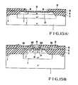
- FIG. 27 A typical example of a conventional high-density, high-speed bipolar transistor for a semiconductor IC as described in Electronics Letter, Vol. 19, No. 8, PP. 283 - 284, April 14, 1983 is illustrated in Fig. 27. Referring to Fig.
- reference numeral 1 denotes a p -type silicon substrate; 2, an n-type epitaxial layer constituting a collector region; 3, an n +- type buried layer; 4A to 4E, oxide films; 5, a p +- type channel cut layer; 6, a base region; 7, a base contact region; 8, an emitter region; 9, an intrinsic transistor region (the region surrounded by a broken line); 10, a base metal electrode; 11, an emitter metal electrode; 12,.a collector metal electrode; 13, a polysilicon electrode layer doped with a p-type impurity; 14A and 14B, polysilicon electrode layers containing an n-type impurity; and 15, a nitride film.
- the region 9 is the region indispensable to transistor operation.
- the base, collector and emitter electrodes constituted by polysilicon layers at positions near the region 9 decreases parasitic capacitances and resistances. However, when isolation of the electrodes and mask alignment margins are taken into consideration, the actual transistor size is larger than the region 9.
- the 1- ⁇ m rule is applied to the example in Fig. 27.
- the emitter electrode constituted by the polysilicon layer 14A and the base electrode constituted by the polysilicon layer 13 are self-aligned and formed on the substrate surface adjacent to each other without degrading transistor characteristics, the distance between the emitter and collector electrodes cannot be decreased since it is determined by a photolithographic pattern rule during formation of the underlying films prior to the formation of electrodes.
- Both the junction capacitance between the p -type silicon substrate 1 and the n -type buried layer 3, serving as the collector region, and the area occupied by the transistor as a whole are increased. High-speed operation and high density cannot be achieved.
- a complicated fabrication process is required.
- the npn and pnp transistors are constituted by vertical and lateral transistors, respectively, the electrical characteristics of the pnp transistor are poor.
- bipolar transistor comprising:
- a method of manufacturing a bipolar transistor including at least the steps of: forming a first insulating film as a field insulating film on a semiconductor substrate having a collector region of a first conductivity type; forming a first nondoped semiconductor layer on the first insulating film; oxidizing the first nondoped semiconductor layer except for a part of the collector region to form a second insulating film; doping an impurity of a second conductivity type in part of a region of the first nondoped semiconductor layer, thereby forming a first doped region; partially etching a part of a nondoped portion of the first nondoped semiconductor layer which is adjacent to the first doped region and located on the collector region, thereby forming a groove in the first nondoped semiconductor layer; doping an impurity of the first conductivity type to form a second doped region in a region of the first nondoped semiconductor layer which excludes the first doped region; side-etching
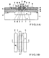
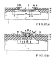
- Figs. 1A shows a vertical npn bipolar transistor according to an embodiment of the present invention when viewed along the line B - B of Fig. 1B and Fig. 1B shows the electrode arrangement thereof.
- the same reference numerals in Figs. 1(A) and 1(B) denote the same parts as in Fig. 27.
- base, collector and emitter electrodes are formed within a single opening defined by an insulating film consisting of an oxide film 4A and a nitride film 15.
- a base electrode connected to a polysilicon layer 13 containing a p-type impurity and a collector electrode connected to a polysilicon layer 14B containing an n-type impurity are formed at edges of the opening.
- An emitter electrode connected to a polysilicon layer 14A containing an n-type impurity is formed between the base and collector electrodes.
- The'base, collector and emitter electrodes are isolated by oxide films 4B, 4D, and 4E. These electrodes are self-aligned in the manner described below.
- the polysilicon layer 14A serves as a diffusion source for forming an emitter region 8.
- the contact widths of the base and collector layers can each be decreased to 0.5 um or less.
- the emitter width can also be easily decreased to 0.5 um or less.
- a collector diffusion layer 16 is formed in the n-type epitaxial layer 2 using the polysilicon layer 14B as a diffusion source.
- FIG. 2(A) to 18(A) An example of the fabrication process of the above bipolar transistor is illustrated in Figs. 2(A) to 18(A), in which Figs. 2 (A) , 3(A),... 18(A) correspond to Fig. 1(A) and Figs. 2(B), 3(B),... 18 (B) correspond to the drawings taken along a line A - A of Fig. 1(B).
- a 1- ⁇ m thick n +- type buried layer 3 having an arsenic concentration of 3 x 10 19 atoms/cm 3 , a 1- ⁇ m thick n-type epitaxial layer 2 having a phosphorus concentration of 1 x 10 16 atoms/cm 3 , and a p + -type channel cut layer 5 are formed in a p -type silicon substrate 1 having a resistivity of 30 to 40 ⁇ cm.
- a thick oxide film (SiO 2 film) 17 is formed by LOCOS (Local Oxidation of Silicon) to 0 flatten the surface.
- a 500-A thick oxide film 17A is 0 formed together with the SiO 2 film 17, and 1500-A thick nitride film (Si 3 N 4 film) 18 is then formed over the entire surface (Figs. 2(A) and 2(B)).
- the thin oxide film 17A and the nitride film 18 constitute the field insulating film.
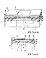
- a 6000- ⁇ thick nondoped polysilicon layer 19 is formed to cover the entire surface of the resultant structure, and an unnecessary region is selectively oxidized to form a 7500-A thick oxide film 20 (Figs. 3(A) 0 0 and 3(B)).
- a 1000-A thick oxide film 21, a 1000-A thick nitride film 22 and a 6000-A thick nondoped polysilicon layer 23 are sequentially formed on the oxide film 20 by CVD (Chemical Vapor Deposition).
- the polysilicon layer 23 and the nitride film 22 are patterned such that one end is located over the n-type epitaxial layer 2 under the thin oxide film 17A to prepare an ion implantation mask (Figs.
- boron ions are implanted as a p-type impurity in the entire surface, they are implanted only in a portion of the polysilicon layer 19 not masked by the polysilicon layer 23 and the nitride film 22, thus forming a boron-doped polysilicon layer 19A having an average boron concentration of 4 x 10 20 atoms/cm 3 .
- the polysilicon layer 23 is also doped with boron ions and converted to boron-doped silicon layer 23A (Figs. 5 (A) and 5(B)). The boron-doped silicon layer 23A is then removed by wet or dry etching.
- the oxide film 21 is side-etched using the nitride film 22 as a mask, so that the surface of the nondoped polysilicon layer 19 is partially exposed.
- the exposed portion is represented by reference numeral 24 (Figs. 6(A) and 6(B)).
- the nondoped polysilicon layer 19 is etched with an etching solution.
- the etching solution is selected such that the etching rate for nondoped polysilicon is about 10 times that for boron-doped polysilicon.
- An example of such an etching solution is potassium hydroxide. This etching forms a 1.5- ⁇ m wide groove 25. The groove 25 determines an active region of the transistor.
- the oxide film 21 is removed (Figs. 7 (A) and 7(B)).
- Thermal oxidation is performed to form a 3000- ⁇ thick oxide film 26.
- a 2- ⁇ m wide window 27 is formed for doping an n-type impurity in the nondoped polysilicon layer 19 (Figs. 8(A) and 8(B)).
- Arsenic or phosphorus as an n-type impurity is ion-implanted or doped by a doped oxide method to convert the nondoped polysilicon layer 19 to an n-type doped polysilicon layer 19B having an impurity concentration of 5 x 10 20 atoms/cm 3 .
- the resultant structure is annealed at a temperature of 900°C for 20 minutes and is oxidized to form an oxide film 28, the thickness of which is about 3000 A.
- a 1500-A nitride film 29 and a 1000-A polysilicon layer 30 are sequentially formed.
- a resist layer (not shown) is formed on the polysilicon layer 30 to sufficiently expose the groove edge portion serving as an active region with respect to the B - B section and to cover the edge of the groove by about 0.5 to 1 ⁇ m with respect to the A - A section.
- a window is formed in the polysilicon layer 30 by a known method such as plasma etching using the resist layer as a mask (Figs. 9(A) and 9(B)).
- 3500 A of the nitride film 29 is side-etched using the polysilicon layer 30 as a mask (Figs. 10(A) and 10(B)), and the polysilicon layer 30 is removed.
- the bottom of the groove serving as the active region is protected by the oxide film 17A, and the polysilicon layers 19A and 19B serving as the base and collector electrodes have not yet been exposed and are protected by the oxide film 28 and the nitride film 18.
- Exposed portions of the nitride films 18 and 2 9 in the groove in the A - A section are etched.
- the nitride film 18 is side-etched, as indicated by reference numerals 31.
- the lower surfaces of the polysilicon layers 19A and 19B serving as the base and 0 collector electrodes are exposed by 2000 A in the B - B section (Fig. 11).
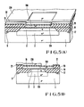
- a 2000-A thick nondoped polysilicon layer 32 is formed by low-pressure CVD on the entire surface to fill the side-etched portions 31 (Figs. 12(A) and 12(B)).
- the silicon layer 32 fills the exposed surface completely, including the side-etched portions 31. Subsequently, the polysilicon layer 32 is removed by isotropic etching. In this case, the side-etched portions 31 are filled by polysilicon layers 32A and 32B in the B - B section. However, the polysilicon layer 32 is not left on the A - A section (Figs. 13(A) and 13(B)). The silicon layer (19A + 32A) is completely isolated from the silicon layer (19B + 32B), as is apparent from Fig. 13B. These layers can be used as independent functional elements as the base and collector electrodes. Therefore, the polysilicon layers as the base and collector electrodes are formed at opposite edges of the single opening. 0
- a 700-A thick oxide film 33 is formed in the inner surface of the groove by thermal oxidation at a temperature of 900°C for 20 minutes.
- impurity ions are diffused from the impurity-doped polysilicon layers 19A and 19B to the nondoped polysilicon layers 32A and 32B contacting the layers 19A and 19B, thereby forming a polysilicon layer 32A' doped with a p-type impurity and a polysilicon layer 32B' doped with an n-type impurity, respectively.
- Boron ions are implanted through the oxide film 33 at an acceleration voltage of 25 keV and a dose of 1.5 x 10 13 ions/cm 2 to form a 2- ⁇ m deep base region 34.
- a 1000-A thick oxide film 35 and a 4500- ⁇ thick polysilicon layer 36 are sequentially formed by CVD to form a self-aligned emitter opening '(Figs. 14(A) and 14(B)).
- the polysilicon layer 36 is removed by an anisotropic etching technique such as RIE (Reactive Ion Etching) to leave portions only on groove side walls (Figs. 15 (A) and 15 (B)) ("Reactive Ion Etching of Aluminum using SiCl 4 ", Journal of Vacuum Science & Technology, Vol. 20, 1982, pp. 186 - 190).
- the oxide films 35 and 33 are sequentially etched by a combination of anisotropic etching and wet etching (for removing the damage inflicted by anisotropic etching) to form an opening and expose a silicon surface portion of the base region 34.
- the oxide films 35 and 33 are anisotropically etched by about 1300 ⁇ and then completely removed by wet etching.
- a 3000-A thick arsenic-doped polysilicon layer 37 having a concentration of 1 x 10 21 atoms/cm 3 is formed to cover the entire surface (Figs. 16(A) and 16(B)). An excess portion of the polysilicon layer 37 is removed by dry etching.
- the resultant structure is then annealed to diffuse the n-type impurity from the polysilicon layer 37 into the monocrystalline silicon of the base region 34, thereby forming a 0.1-pm deep emitter diffusion region 38.
- the polysilicon layers 19B and 32B act as diffusion sources to form a collector contact diffusion region 39.
- the polysilicon layers 19A and 32A act as diffusion sources to form a base contact region 40.
- Arsenic is also diffused in the polysilicon layer 36 contacting the polysilicon layer-37 to form an arsenic-doped polysilicon layer 36A.
- base and collector contact windows 41 and 42 are formed in the oxide film 28 (Figs. 17(A) and 17(B)).
- An oxide film 43 is formed by CVD to cover the entire surface, and emitter, base, and collector contact windows are opened.
- Collector, emitter, and base metal electrodes 44, 45, and 46 of a metal such as aluminum are formed (Figs. 18(A) and 18(B)).
- W F denotes the width of a base edge region in the A - A section
- W CC the width of the collector contact diffusion region 39
- WEC the width of the emitter diffusion region 38
- W BOC the width of the base contact region
- W BC the width of the base region 34
- W F ' the width of the base edge region in the B - B section
- W E the width of the emitter diffusion window
- W C the width of the collector contact diffusion window
- W B the width of the base contact diffusion window
- W OX1 the distance between the emitter diffusion window and the collector contact diffusion window
- W OX2 the distance between the emitter diffusion window and the base contact diffusion window.
- W OX1 is substantially equal to W OX2 , 0.5 ⁇ m or less, and the same as the thickness of the oxide film 28.
- Fig. 19 shows a sectional structure when the interface between the semiconductor substrate and the polysilicon layer and insulating film is viewed from the top.
- the region 100 surrounded by the short broken line represents the base region excluding the base contact diffusion region
- the region surrounded by the alternate long and short dashed line 101 represents the emitter region
- the region surrounded by the long broken line 102 represents the diffusion region formed by diffusion from the p + -type polysilicon
- the region surrounded by the alternate long and two short dashed line 103 represents the diffusion region formed by diffusion from the n +- type polysilicon.
- the regions 104, 105 filled with crosses represent n +- type polysilicon portions, i.e., the polysilicon layer 37 as the emitter electrode region and the polysilicon layer 32B' as the collector electrode region.
- the region 106 filled with dots represents a p + -type polysilicon portion, i.e., the polysilicon layer 32A' as the base region.
- Hatched regions 107 represent the oxide films for insulating the above layers and portions.
- the solid line in Fig. 19 indicates a boundary between the substrate and the polysilicon and oxide films.
- the collector contact diffusion region and the emitter diffusion region are self-aligned with the base contact diffusion region.
- the base and collector electrodes sandwiching the emitter oppose each other, and all are formed in the single opening.
- the distances from the emitter electrode to the base and collector electrodes are the same and very short.
- the area occupied by the transistor and its collector-substrate capacitance are reduced, and high-speed operation can be achieved compared to the conventional structure of Fig. 27.
- npn transistor n-type and p-type conductivities can be interchanged to form a pnp transistor in the same manner as described above.
- the pnp transistor can be formed together with the npn transistor on a single substrate with a small number of changes and additional steps.
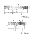
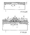
- a pnp transistor is illustrated in Figs. 20 and 21.
- Figs. 20 and 21 are sectional views taken along the line B - B of Fig. 1(B).
- a p-type impurity is implanted in an n-type epitaxial layer 2 through a thin oxide film to form a p-type epitaxial layer 51 for the pnp transistor.
- a thin oxide film 17A and a nitride film 18 are formed (Fig. 20).
- the subsequent steps are the same as those in the fabrication of an npn transistor until the formation of the thin oxide film 33 in Figs. 14 (A) and 14(B).
- Phosphorus ions are implanted through the oxide film 33 to form a base region 52.
- An oxide film 35 and a polysilicon layer 57 are sequentially formed.
- the polysilicon layer 57 is partially removed by anisotropic etching, and the oxide film 35 is partially etched by a combination of anisotropic etching and wet etching to expose a silicon surface portion serving as an emitter region 53.
- a boron-doped polysilicon layer 56 is formed and boron is diffused by annealing to form an emitter diffusion region 53.
- a collector contact diffusion region 54 and a base contact region 55 are formed.
- the subsequent steps are the same as those in the fabrication process of the npn transistor.
- a finished structure with metal electrodes is illustrated in Fig. 21.
- Reference numerals 56 and 57 denote p-type impurity, i.e., boron-doped polysilicon layers serving as the emitter electrode.
- Polysilicon layers 19A and 32A doped with a p-type impurity constitute the collector electrode, and polysilicon layers 19B and 32B doped with an n-type impurity constitute the base electrode.
- the vertical pnp and npn transistors can be easily formed on a single chip to constitute a high-performance complementary bipolar transistor.
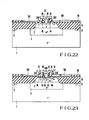
- the electrodes are made of polycrystalline silicon. However, part or all of polysilicon may be replaced with a silicide. Alternatively, a metal may be selectively grown on only monocrystalline or polycrystalline silicon to constitute part of the electrodes.
- Figs. 22 to 24 show still another embodiment in which part of polysilicon is replaced with a silicide.
- Figs. 22 to 24 are sectional views taken along the line B - B of Fig. KB).
- a polysilicon layer 37 doped with an n-type impurity is formed and etching is performed using the resultant layer as an etching mask to expose the surfaces of the p-type polysilicon layer 19A serving as the base electrode region and the n-type polysilicon layer 19B serving as the collector electrode region (Fig. 22).
- Subsequent annealing produces an emitter diffusion region 38.
- An oxide film 61 is formed by CVD and etched by anisotropic etching to leave it around only the emitter region (Fig. 23).
- a metal layer such as a Pt layer is formed and alloyed with silicon by annealing to constitute a silicide layer 62.
- a nonalloyed metal layer on the oxide film is removed (Fig. 24), and an oxide film 43 is formed and etched to form contact holes.
- collector, emitter, and base metal electrodes 63, 64, and 65 of aluminum are formed (Fig. 25).
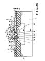
- Fig. 26 shows still another embodiment employing selective growth of a metal.
- a metal layer 71 is selectively grown on the surfaces of the polysilicon layers 19A, 19B, and 37 exposed in the step shown in Fig. 23.
- a thick metal layer of aluminum is formed and patterned to constitute collector, emitter and base metal electrodes 72, 73, and 74.
- the n -type buried layer 3 is formed in the substrate.
- the present invention is also applicable if the substrate does not have an n +- type buried layer.
- the thick oxide film 17 is formed.
- the present invention is also applicable when such a film is not formed.
- the collector and base electrodes are formed within a single opening, and the emitter electrode is formed between the collector and base electrodes within the single opening.
- the electrodes are isolated by insulating interlayers.
- the area occupied by the transistor can be decreased to 1/2 that of the conventional structure. For this reason, a high-density, high-integration LSI can be fabricated. Since the collector-substrate capacitance is decreased, high-speed operation can be achieved.
- Polysilicon or a silicide is used to constitute the electrode regions, so that the emitter, base, and collector regions are connected to the metal electrodes through polysilicon or silicide.
- the emitter, base, and collector regions are therefore free from Schottky tunneling, and stable high-speed operation is guaranteed even with shallow junctions.
- High-performance vertical pnp and npn transistors can be easily formed on a single chip. Because of complicated fabrication processes or the use of a lateral pnp transistor with poor characteristics in place of a vertical pnp transistor to avoid such processes, complementary bipolar LSIs with vertical transistors have . not received a great deal of attention.
- the present invention can provide a high-speed complementary bipolar LSI with low power consumption.
- a semiconductor layer of an SOS structure can be used in place of the semiconductor substrate.
Abstract
Description
- The present invention relates to a bipolar transistor used in various semiconductor integrated circuits or the like and a method of manufacturing the same and, more particularly, to a vertical bipolar transistor and a method of manufacturing the same.
- A typical example of a conventional high-density, high-speed bipolar transistor for a semiconductor IC as described in Electronics Letter, Vol. 19, No. 8, PP. 283 - 284, April 14, 1983 is illustrated in Fig. 27. Referring to Fig. 27,
reference numeral 1 denotes a p -type silicon substrate; 2, an n-type epitaxial layer constituting a collector region; 3, an n+-type buried layer; 4A to 4E, oxide films; 5, a p+-type channel cut layer; 6, a base region; 7, a base contact region; 8, an emitter region; 9, an intrinsic transistor region (the region surrounded by a broken line); 10, a base metal electrode; 11, an emitter metal electrode; 12,.a collector metal electrode; 13, a polysilicon electrode layer doped with a p-type impurity; 14A and 14B, polysilicon electrode layers containing an n-type impurity; and 15, a nitride film. - With the structure in Fig. 27, the
region 9 is the region indispensable to transistor operation. - Formation of the base, collector and emitter electrodes constituted by polysilicon layers at positions near the
region 9 decreases parasitic capacitances and resistances. However, when isolation of the electrodes and mask alignment margins are taken into consideration, the actual transistor size is larger than theregion 9. The 1-µm rule is applied to the example in Fig. 27. Although the emitter electrode constituted by thepolysilicon layer 14A and the base electrode constituted by thepolysilicon layer 13 are self-aligned and formed on the substrate surface adjacent to each other without degrading transistor characteristics, the distance between the emitter and collector electrodes cannot be decreased since it is determined by a photolithographic pattern rule during formation of the underlying films prior to the formation of electrodes. Both the junction capacitance between the p -type silicon substrate 1 and the n -type buriedlayer 3, serving as the collector region, and the area occupied by the transistor as a whole are increased. High-speed operation and high density cannot be achieved. In order to form vertical npn and pnp transistors on a single substrate to prepare a complimentary bipolar transistor in the same manner as the vertical npn transistor in Fig. 1, a complicated fabrication process is required. On the other hand, if the npn and pnp transistors are constituted by vertical and lateral transistors, respectively, the electrical characteristics of the pnp transistor are poor. - It is, therefore, a principal object of the present invention to provide a bipolar transistor wherein a transistor area can be significantly reduced.
- It is another object of the present invention to provide a method of manufacturing the above bipolar transistor.
- It is still another object of the present invention to provide a high-speed bipolar transistor.
- It is still another object of the present invention to provide a method of manufacturing the above bipolar transistor.
- bipolar transistor comprising:
- According to an aspect of the present invention to provide a bipolar transistor comprising: a collector region consisting of a first semiconductor region of a first conductivity type, the collector region being formed in contact with a surface of a semiconductor layer; a base region consisting of a second semiconductor region of a second conductivity type formed within the collector region to be in contact with the surface of the semiconductor layer; an emitter region consisting of a third semiconductor region of the first conductivity type formed within the base region to be in contact with the surface of the semiconductor layer; collector and base electrodes connected to the collector and base regions at opposite edges of a single opening formed in a field insulating film covering the surface of the semiconductor layer, the collector and base electrodes consisting of a conductor; an emitter electrode connected to the emitter region and consisting of a conductor; a first insulating interlayer formed between the collector electrode and the emitter electrode; and a second insulating interlayer formed between the emitter electrode and the base electrode, wherein a distance between the collector and emitter electrodes on the surface of the semiconductor layer is substantially the same as that between the emitter electrode and the base electrode.
- According to another aspect of the present invention to provide a method of manufacturing a bipolar transistor, including at least the steps of: forming a first insulating film as a field insulating film on a semiconductor substrate having a collector region of a first conductivity type; forming a first nondoped semiconductor layer on the first insulating film; oxidizing the first nondoped semiconductor layer except for a part of the collector region to form a second insulating film; doping an impurity of a second conductivity type in part of a region of the first nondoped semiconductor layer, thereby forming a first doped region; partially etching a part of a nondoped portion of the first nondoped semiconductor layer which is adjacent to the first doped region and located on the collector region, thereby forming a groove in the first nondoped semiconductor layer; doping an impurity of the first conductivity type to form a second doped region in a region of the first nondoped semiconductor layer which excludes the first doped region; side-etching the first insulating film in the groove excluding a vicinity of the second insulating film to expose parts of lower surfaces of the second doped semiconductor layer of the first conductivity type and the first doped semiconductor layer of the second conductivity type; filling side-etched portions with a second semiconductor layer; doping an impurity of the second conductivity type in a surface of the collector region in the groove to form a base region; forming a third insulating film and a third semiconductor layer on the entire surface; removing the third insulating film and the third semiconductor layer except for portions on side wall of the groove by using anisotropic etching to expose a surface of the base region at the center of the groove; forming a fourth semiconductor layer containing an impurity of the first conductivity type on the surface of the base region and in a region surrounded by the third insulating film and the third semiconductor layer; and diffusing the impurity of the first conductivity type from the fourth semiconductor layer into the base region to form an emitter region.
-
- Fig. 1(A) is a sectional view showing an npn bipolar transistor according to an embodiment of the present invention;
- Fig. 1(B) is a plan view of the transistor in Fig. 1(A);
- Figs. 2(A) to 18(B) show the steps for manufacturing the bipolar transistor in Fig. 1(A), in which Figs. 2(A), 3(A),... 8(A) are sectional perspective views thereof and Figs. 2(B), 3(B),... 8(B), 9(A),... 18 (B) are sectional views thereof;
- Fig. 19 is a sectional view of the transistor in Fig. 1(A) taken along a-direction different from that in Fig. 1(A);
- Figs. 20 and 21 are sectional views showing the steps for manufacturing a bipolar transistor according to another embodiment of the present invention;
- Figs. 22 to 25 are sectional views showing a bipolar transistor according to still another embodiment of the present invention;
- Fig. 26 is a sectional view showing a bipolar transistor according to still another embodiment of the present invention; and
- Fig. 27 is a sectional view showing a conventional bipolar transistor.
- Figs. 1A shows a vertical npn bipolar transistor according to an embodiment of the present invention when viewed along the line B - B of Fig. 1B and Fig. 1B shows the electrode arrangement thereof. The same reference numerals in Figs. 1(A) and 1(B) denote the same parts as in Fig. 27. As is apparent from comparison between Fig. 27 and Figs. 1(A) and 1(B), in this embodiment, base, collector and emitter electrodes are formed within a single opening defined by an insulating film consisting of an
oxide film 4A and anitride film 15. More specifically, a base electrode connected to apolysilicon layer 13 containing a p-type impurity and a collector electrode connected to apolysilicon layer 14B containing an n-type impurity are formed at edges of the opening. An emitter electrode connected to apolysilicon layer 14A containing an n-type impurity is formed between the base and collector electrodes. The'base, collector and emitter electrodes are isolated byoxide films polysilicon layer 14A serves as a diffusion source for forming anemitter region 8. The contact widths of the base and collector layers can each be decreased to 0.5 um or less. The emitter width can also be easily decreased to 0.5 um or less. Distances between the emitter and base contacts and between the emitter and collector contacts can be substantially the same and 0.5 pm or less each. The overall width of the transistor including the emitter, collector and base electrodes can be decreased to about 1/2 that of the conventional structure, and regions unnecessary for transistor operation can be minimized. Base-collector and collector-substrate capacitances can be reduced to achieve high-speed operation of the bipolar transistor. Acollector diffusion layer 16 is formed in the n-typeepitaxial layer 2 using thepolysilicon layer 14B as a diffusion source. - An example of the fabrication process of the above bipolar transistor is illustrated in Figs. 2(A) to 18(A), in which Figs. 2 (A) , 3(A),... 18(A) correspond to Fig. 1(A) and Figs. 2(B), 3(B),... 18 (B) correspond to the drawings taken along a line A - A of Fig. 1(B).
- A 1-µm thick n+-type buried
layer 3 having an arsenic concentration of 3 x 10¹⁹ atoms/cm3, a 1-µm thick n-typeepitaxial layer 2 having a phosphorus concentration of 1 x 10¹⁶ atoms/cm3, and a p+-typechannel cut layer 5 are formed in a p -type silicon substrate 1 having a resistivity of 30 to 40 Ω·cm. A thick oxide film (SiO2 film) 17 is formed by LOCOS (Local Oxidation of Silicon) to 0 flatten the surface. A 500-Athick oxide film 17A is 0 formed together with the SiO2 film 17, and 1500-A thick nitride film (Si3N4 film) 18 is then formed over the entire surface (Figs. 2(A) and 2(B)). Thethin oxide film 17A and thenitride film 18 constitute the field insulating film. - A 6000-Å thick
nondoped polysilicon layer 19 is formed to cover the entire surface of the resultant structure, and an unnecessary region is selectively oxidized to form a 7500-A thick oxide film 20 (Figs. 3(A) 0 0 and 3(B)). A 1000-Athick oxide film 21, a 1000-Athick nitride film 22 and a 6000-A thicknondoped polysilicon layer 23 are sequentially formed on theoxide film 20 by CVD (Chemical Vapor Deposition). Thepolysilicon layer 23 and thenitride film 22 are patterned such that one end is located over the n-typeepitaxial layer 2 under thethin oxide film 17A to prepare an ion implantation mask (Figs. 4(A) and 4(B)). When boron ions are implanted as a p-type impurity in the entire surface, they are implanted only in a portion of thepolysilicon layer 19 not masked by thepolysilicon layer 23 and thenitride film 22, thus forming a boron-dopedpolysilicon layer 19A having an average boron concentration of 4 x 10²⁰ atoms/cm3. Thepolysilicon layer 23 is also doped with boron ions and converted to boron-dopedsilicon layer 23A (Figs. 5 (A) and 5(B)). The boron-dopedsilicon layer 23A is then removed by wet or dry etching. 0.2 µm of theoxide film 21 is side-etched using thenitride film 22 as a mask, so that the surface of thenondoped polysilicon layer 19 is partially exposed. The exposed portion is represented by reference numeral 24 (Figs. 6(A) and 6(B)). After thenitride film 22 is removed. thenondoped polysilicon layer 19 is etched with an etching solution. The etching solution is selected such that the etching rate for nondoped polysilicon is about 10 times that for boron-doped polysilicon. An example of such an etching solution is potassium hydroxide. This etching forms a 1.5-µmwide groove 25. Thegroove 25 determines an active region of the transistor. Subsequently, theoxide film 21 is removed (Figs. 7 (A) and 7(B)). - Thermal oxidation is performed to form a 3000-Å
thick oxide film 26. A 2-µmwide window 27 is formed for doping an n-type impurity in the nondoped polysilicon layer 19 (Figs. 8(A) and 8(B)). Arsenic or phosphorus as an n-type impurity is ion-implanted or doped by a doped oxide method to convert thenondoped polysilicon layer 19 to an n-type dopedpolysilicon layer 19B having an impurity concentration of 5 x 10²⁰ atoms/cm3. The resultant structure is annealed at a temperature of 900°C for 20 minutes and is oxidized to form anoxide film 28, the thickness of which is about 3000 A. A 1500-A nitride film 29 and a 1000-A polysilicon layer 30 are sequentially formed. A resist layer (not shown) is formed on thepolysilicon layer 30 to sufficiently expose the groove edge portion serving as an active region with respect to the B - B section and to cover the edge of the groove by about 0.5 to 1 µm with respect to the A - A section. A window is formed in thepolysilicon layer 30 by a known method such as plasma etching using the resist layer as a mask (Figs. 9(A) and 9(B)). 3500 A of thenitride film 29 is side-etched using thepolysilicon layer 30 as a mask (Figs. 10(A) and 10(B)), and thepolysilicon layer 30 is removed. At this point, the bottom of the groove serving as the active region is protected by theoxide film 17A, and thepolysilicon layers oxide film 28 and thenitride film 18. - Exposed portions of the
nitride films nitride film 18 is side-etched, as indicated byreference numerals 31. The lower surfaces of thepolysilicon layers oxide film o 17A, a 2000-A thicknondoped polysilicon layer 32 is formed by low-pressure CVD on the entire surface to fill the side-etched portions 31 (Figs. 12(A) and 12(B)). Since the polysilicon layer formed by low-pressure CVD is grown isotropically from the exposed surface, thesilicon layer 32 fills the exposed surface completely, including the side-etchedportions 31. Subsequently, thepolysilicon layer 32 is removed by isotropic etching. In this case, the side-etchedportions 31 are filled bypolysilicon layers polysilicon layer 32 is not left on the A - A section (Figs. 13(A) and 13(B)). The silicon layer (19A + 32A) is completely isolated from the silicon layer (19B + 32B), as is apparent from Fig. 13B. These layers can be used as independent functional elements as the base and collector electrodes. Therefore, the polysilicon layers as the base and collector electrodes are formed at opposite edges of the single opening. 0 - A 700-A
thick oxide film 33 is formed in the inner surface of the groove by thermal oxidation at a temperature of 900°C for 20 minutes. By this process, impurity ions are diffused from the impurity-dopedpolysilicon layers nondoped polysilicon layers layers polysilicon layer 32A' doped with a p-type impurity and apolysilicon layer 32B' doped with an n-type impurity, respectively. Boron ions are implanted through theoxide film 33 at an acceleration voltage of 25 keV and a dose of 1.5 x 10¹³ ions/cm2 to form a 2-µmdeep base region 34. A 1000-Athick oxide film 35 and a 4500-Åthick polysilicon layer 36 are sequentially formed by CVD to form a self-aligned emitter opening '(Figs. 14(A) and 14(B)). Thepolysilicon layer 36 is removed by an anisotropic etching technique such as RIE (Reactive Ion Etching) to leave portions only on groove side walls (Figs. 15 (A) and 15 (B)) ("Reactive Ion Etching of Aluminum using SiCl4", Journal of Vacuum Science & Technology, Vol. 20, 1982, pp. 186 - 190). Theoxide films base region 34. Theoxide films polysilicon layer 37 having a concentration of 1 x 10²¹ atoms/cm3 is formed to cover the entire surface (Figs. 16(A) and 16(B)). An excess portion of thepolysilicon layer 37 is removed by dry etching. The resultant structure is then annealed to diffuse the n-type impurity from thepolysilicon layer 37 into the monocrystalline silicon of thebase region 34, thereby forming a 0.1-pm deepemitter diffusion region 38. In this step, the polysilicon layers 19B and 32B act as diffusion sources to form a collectorcontact diffusion region 39. Similarly, thepolysilicon layers base contact region 40. Arsenic is also diffused in thepolysilicon layer 36 contacting the polysilicon layer-37 to form an arsenic-dopedpolysilicon layer 36A. Subsequently, base andcollector contact windows oxide film 43 is formed by CVD to cover the entire surface, and emitter, base, and collector contact windows are opened. Collector, emitter, andbase metal electrodes - The structural parameters of the prepared bipolar transistor are defined in Figs. 18(A) and 18(B). Reference symbol WF denotes the width of a base edge region in the A - A section; WCC, the width of the collector
contact diffusion region 39; WEC, the width of theemitter diffusion region 38; WBOC, the width of the base contact region; WBC, the width of thebase region 34; WF', the width of the base edge region in the B - B section; WE, the width of the emitter diffusion window; WC, the width of the collector contact diffusion window; WB, the width of the base contact diffusion window; WOX1, the distance between the emitter diffusion window and the collector contact diffusion window; and WOX2, the distance between the emitter diffusion window and the base contact diffusion window. WOX1 is substantially equal to WOX2, 0.5 µm or less, and the same as the thickness of theoxide film 28. - Fig. 19 shows a sectional structure when the interface between the semiconductor substrate and the polysilicon layer and insulating film is viewed from the top. The
region 100 surrounded by the short broken line represents the base region excluding the base contact diffusion region, the region surrounded by the alternate long and short dashedline 101 represents the emitter region, the region surrounded by the long brokenline 102 represents the diffusion region formed by diffusion from the p+-type polysilicon, and the region surrounded by the alternate long and two short dashedline 103 represents the diffusion region formed by diffusion from the n+-type polysilicon. Theregions polysilicon layer 37 as the emitter electrode region and thepolysilicon layer 32B' as the collector electrode region. Theregion 106 filled with dots represents a p+-type polysilicon portion, i.e., thepolysilicon layer 32A' as the base region. Hatchedregions 107 represent the oxide films for insulating the above layers and portions. The solid line in Fig. 19 indicates a boundary between the substrate and the polysilicon and oxide films. - As is apparent from Fig. 19, the collector contact diffusion region and the emitter diffusion region are self-aligned with the base contact diffusion region. The base and collector electrodes sandwiching the emitter oppose each other, and all are formed in the single opening. The distances from the emitter electrode to the base and collector electrodes are the same and very short. The area occupied by the transistor and its collector-substrate capacitance are reduced, and high-speed operation can be achieved compared to the conventional structure of Fig. 27.
- The above embodiment exemplifies an npn transistor. However, n-type and p-type conductivities can be interchanged to form a pnp transistor in the same manner as described above. The pnp transistor can be formed together with the npn transistor on a single substrate with a small number of changes and additional steps. A pnp transistor is illustrated in Figs. 20 and 21. Figs. 20 and 21 are sectional views taken along the line B - B of Fig. 1(B).
- A p-type impurity is implanted in an n-
type epitaxial layer 2 through a thin oxide film to form a p-type epitaxial layer 51 for the pnp transistor. After LOCOS is performed, athin oxide film 17A and anitride film 18 are formed (Fig. 20). The subsequent steps are the same as those in the fabrication of an npn transistor until the formation of thethin oxide film 33 in Figs. 14 (A) and 14(B). Phosphorus ions are implanted through theoxide film 33 to form abase region 52. Anoxide film 35 and a polysilicon layer 57 are sequentially formed. The polysilicon layer 57 is partially removed by anisotropic etching, and theoxide film 35 is partially etched by a combination of anisotropic etching and wet etching to expose a silicon surface portion serving as anemitter region 53. A boron-doped polysilicon layer 56 is formed and boron is diffused by annealing to form anemitter diffusion region 53. At the same time, a collectorcontact diffusion region 54 and abase contact region 55 are formed. The subsequent steps are the same as those in the fabrication process of the npn transistor. A finished structure with metal electrodes is illustrated in Fig. 21. Reference numerals 56 and 57 denote p-type impurity, i.e., boron-doped polysilicon layers serving as the emitter electrode.Polysilicon layers polysilicon layers - The vertical pnp and npn transistors can be easily formed on a single chip to constitute a high-performance complementary bipolar transistor.
- In the above embodiments, the electrodes are made of polycrystalline silicon. However, part or all of polysilicon may be replaced with a silicide. Alternatively, a metal may be selectively grown on only monocrystalline or polycrystalline silicon to constitute part of the electrodes.
- Figs. 22 to 24 show still another embodiment in which part of polysilicon is replaced with a silicide. Figs. 22 to 24 are sectional views taken along the line B - B of Fig. KB). A
polysilicon layer 37 doped with an n-type impurity is formed and etching is performed using the resultant layer as an etching mask to expose the surfaces of the p-type polysilicon layer 19A serving as the base electrode region and the n-type polysilicon layer 19B serving as the collector electrode region (Fig. 22). Subsequent annealing produces anemitter diffusion region 38. Anoxide film 61 is formed by CVD and etched by anisotropic etching to leave it around only the emitter region (Fig. 23). A metal layer such as a Pt layer is formed and alloyed with silicon by annealing to constitute asilicide layer 62. A nonalloyed metal layer on the oxide film is removed (Fig. 24), and anoxide film 43 is formed and etched to form contact holes. Finally, collector, emitter, andbase metal electrodes - Fig. 26 shows still another embodiment employing selective growth of a metal. A
metal layer 71 is selectively grown on the surfaces of the polysilicon layers 19A, 19B, and 37 exposed in the step shown in Fig. 23. After contact holes are formed in theoxide film 43, a thick metal layer of aluminum is formed and patterned to constitute collector, emitter andbase metal electrodes layer 3 is formed in the substrate. However, the present invention is also applicable if the substrate does not have an n+-type buried layer. In the above embodiment, thethick oxide film 17 is formed. However, the present invention is also applicable when such a film is not formed. - According to the present invention as described above, the collector and base electrodes are formed within a single opening, and the emitter electrode is formed between the collector and base electrodes within the single opening. The electrodes are isolated by insulating interlayers. The area occupied by the transistor can be decreased to 1/2 that of the conventional structure. For this reason, a high-density, high-integration LSI can be fabricated. Since the collector-substrate capacitance is decreased, high-speed operation can be achieved. Polysilicon or a silicide is used to constitute the electrode regions, so that the emitter, base, and collector regions are connected to the metal electrodes through polysilicon or silicide. The emitter, base, and collector regions are therefore free from Schottky tunneling, and stable high-speed operation is guaranteed even with shallow junctions. High-performance vertical pnp and npn transistors can be easily formed on a single chip. Because of complicated fabrication processes or the use of a lateral pnp transistor with poor characteristics in place of a vertical pnp transistor to avoid such processes, complementary bipolar LSIs with vertical transistors have . not received a great deal of attention. The present invention, however, can provide a high-speed complementary bipolar LSI with low power consumption. A semiconductor layer of an SOS structure can be used in place of the semiconductor substrate.
Claims (12)
wherein a distance between said collector and emitter electrodes on the surface of said semiconductor layer is substantially the same as that between said emitter electrode and said base electrode.
the step of exposing the lower surface of said first semiconductor layer comprises the steps of:
Applications Claiming Priority (2)
| Application Number | Priority Date | Filing Date | Title |
|---|---|---|---|
| JP60096422A JPH0658912B2 (en) | 1985-05-07 | 1985-05-07 | Bipolar transistor manufacturing method |
| JP96422/85 | 1985-05-07 |
Related Child Applications (2)
| Application Number | Title | Priority Date | Filing Date |
|---|---|---|---|
| EP19900250256 Division EP0409370A3 (en) | 1985-05-07 | 1986-05-07 | Bipolar transistor |
| EP90250256.6 Division-Into | 1986-05-07 |
Publications (3)
| Publication Number | Publication Date |
|---|---|
| EP0201867A2 true EP0201867A2 (en) | 1986-11-20 |
| EP0201867A3 EP0201867A3 (en) | 1987-05-27 |
| EP0201867B1 EP0201867B1 (en) | 1991-06-19 |
Family
ID=14164544
Family Applications (1)
| Application Number | Title | Priority Date | Filing Date |
|---|---|---|---|
| EP86106270A Expired - Lifetime EP0201867B1 (en) | 1985-05-07 | 1986-05-07 | Method of manufacturing a bipolar transistor |
Country Status (6)
| Country | Link |
|---|---|
| US (1) | US4780427A (en) |
| EP (1) | EP0201867B1 (en) |
| JP (1) | JPH0658912B2 (en) |
| KR (1) | KR900008651B1 (en) |
| CA (1) | CA1241458A (en) |
| DE (1) | DE3679862D1 (en) |
Cited By (3)
| Publication number | Priority date | Publication date | Assignee | Title |
|---|---|---|---|---|
| EP0362104A1 (en) * | 1988-08-31 | 1990-04-04 | International Business Machines Corporation | Bipolar transistor integrated circuit technology |
| US5026663A (en) * | 1989-07-21 | 1991-06-25 | Motorola, Inc. | Method of fabricating a structure having self-aligned diffused junctions |
| FR2672733A1 (en) * | 1991-02-13 | 1992-08-14 | France Telecom | IMPROVEMENT IN THE COLLECTOR OF A BIPOLAR TRANSISTOR COMPATIBLE WITH MOS TECHNOLOGY. |
Families Citing this family (18)
| Publication number | Priority date | Publication date | Assignee | Title |
|---|---|---|---|---|
| US4812417A (en) * | 1986-07-30 | 1989-03-14 | Mitsubishi Denki Kabushiki Kaisha | Method of making self aligned external and active base regions in I.C. processing |
| JPS63128750A (en) * | 1986-11-19 | 1988-06-01 | Toshiba Corp | Semiconductor device |
| JPS63193562A (en) * | 1987-02-06 | 1988-08-10 | Toshiba Corp | Manufacture of bipolar transistor |
| DE3825701A1 (en) * | 1987-07-29 | 1989-02-09 | Toshiba Kawasaki Kk | METHOD FOR PRODUCING A BIPOLAR TRANSISTOR |
| US4829025A (en) * | 1987-10-02 | 1989-05-09 | Advanced Micro Devices, Inc. | Process for patterning films in manufacture of integrated circuit structures |
| US4946798A (en) * | 1988-02-09 | 1990-08-07 | Oki Electric Industry Co., Ltd. | Semiconductor integrated circuit fabrication method |
| JPH027529A (en) * | 1988-06-27 | 1990-01-11 | Nec Corp | Bipolar transistor and its manufacture |
| US5064772A (en) * | 1988-08-31 | 1991-11-12 | International Business Machines Corporation | Bipolar transistor integrated circuit technology |
| GB2236901A (en) * | 1989-09-20 | 1991-04-17 | Philips Nv | A method of manufacturing a semiconductor device |
| KR100200397B1 (en) * | 1990-07-23 | 1999-06-15 | 야스카와 히데아키 | Semiconductor device and manufacturing method of the same |
| US5071780A (en) * | 1990-08-27 | 1991-12-10 | Taiwan Semiconductor Manufacturing Company, Ltd. | Reverse self-aligned transistor integrated circuit |
| US5389561A (en) * | 1991-12-13 | 1995-02-14 | Sony Corporation | Method for making SOI type bipolar transistor |
| JP3156436B2 (en) * | 1993-04-05 | 2001-04-16 | 日本電気株式会社 | Heterojunction bipolar transistor |
| JP3307489B2 (en) | 1993-12-09 | 2002-07-24 | 三菱電機株式会社 | Semiconductor device and manufacturing method thereof |
| US5465006A (en) * | 1994-07-15 | 1995-11-07 | Hewlett-Packard Company | Bipolar stripe transistor structure |
| US5932922A (en) * | 1994-08-08 | 1999-08-03 | Semicoa Semiconductors | Uniform current density and high current gain bipolar transistor |
| JPH09199513A (en) * | 1996-01-19 | 1997-07-31 | Mitsubishi Electric Corp | Bipolar transistor and semiconductor device having the bipolar transistor |
| AT2489U1 (en) * | 1997-11-20 | 1998-11-25 | Avl List Gmbh | PISTON PISTON INTERNAL COMBUSTION ENGINE |
Citations (1)
| Publication number | Priority date | Publication date | Assignee | Title |
|---|---|---|---|---|
| US4483726A (en) * | 1981-06-30 | 1984-11-20 | International Business Machines Corporation | Double self-aligned fabrication process for making a bipolar transistor structure having a small polysilicon-to-extrinsic base contact area |
Family Cites Families (10)
| Publication number | Priority date | Publication date | Assignee | Title |
|---|---|---|---|---|
| US3600651A (en) * | 1969-12-08 | 1971-08-17 | Fairchild Camera Instr Co | Bipolar and field-effect transistor using polycrystalline epitaxial deposited silicon |
| US3611067A (en) * | 1970-04-20 | 1971-10-05 | Fairchild Camera Instr Co | Complementary npn/pnp structure for monolithic integrated circuits |
| US4106051A (en) * | 1972-11-08 | 1978-08-08 | Ferranti Limited | Semiconductor devices |
| FR2340619A1 (en) * | 1976-02-04 | 1977-09-02 | Radiotechnique Compelec | IMPROVEMENT IN THE MANUFACTURING PROCESS OF SEMICONDUCTOR DEVICES AND DEVICES THUS OBTAINED |
| JPS53132275A (en) * | 1977-04-25 | 1978-11-17 | Nippon Telegr & Teleph Corp <Ntt> | Semiconductor device and its production |
| US4160991A (en) * | 1977-10-25 | 1979-07-10 | International Business Machines Corporation | High performance bipolar device and method for making same |
| US4157269A (en) * | 1978-06-06 | 1979-06-05 | International Business Machines Corporation | Utilizing polysilicon diffusion sources and special masking techniques |
| JPS587862A (en) * | 1981-06-30 | 1983-01-17 | インタ−ナシヨナル・ビジネス・マシ−ンズ・コ−ポレ−シヨン | Bipolar transistor structure and method of producing same |
| JPS5898964A (en) * | 1981-12-08 | 1983-06-13 | Matsushita Electric Ind Co Ltd | Semiconductor device and manufacture thereof |
| US4431460A (en) * | 1982-03-08 | 1984-02-14 | International Business Machines Corporation | Method of producing shallow, narrow base bipolar transistor structures via dual implantations of selected polycrystalline layer |
-
1985
- 1985-05-07 JP JP60096422A patent/JPH0658912B2/en not_active Expired - Lifetime
-
1986
- 1986-05-02 CA CA000508270A patent/CA1241458A/en not_active Expired
- 1986-05-07 EP EP86106270A patent/EP0201867B1/en not_active Expired - Lifetime
- 1986-05-07 DE DE8686106270T patent/DE3679862D1/en not_active Expired - Lifetime
- 1986-05-07 KR KR8603554A patent/KR900008651B1/en not_active IP Right Cessation
-
1987
- 1987-09-29 US US07/104,544 patent/US4780427A/en not_active Expired - Lifetime
Patent Citations (1)
| Publication number | Priority date | Publication date | Assignee | Title |
|---|---|---|---|---|
| US4483726A (en) * | 1981-06-30 | 1984-11-20 | International Business Machines Corporation | Double self-aligned fabrication process for making a bipolar transistor structure having a small polysilicon-to-extrinsic base contact area |
Non-Patent Citations (2)
| Title |
|---|
| IBM TECHNICAL DISCLOSURE BULLETIN, vol. 23, no. 12, May 1981, pages 5384-5387, New York, US; C.G. JAMBOTKAR "Compact NPN transistors" * |
| JAPANESE JOURNAL OF APPLIED PHYSICS, supplement 20-1, 1981, pages 155-159, Tokyo, JP; T. SAKAI et al.: "High speed bipolar ICs super self-aligned process technology" * |
Cited By (7)
| Publication number | Priority date | Publication date | Assignee | Title |
|---|---|---|---|---|
| EP0362104A1 (en) * | 1988-08-31 | 1990-04-04 | International Business Machines Corporation | Bipolar transistor integrated circuit technology |
| US4967253A (en) * | 1988-08-31 | 1990-10-30 | International Business Machines Corporation | Bipolar transistor integrated circuit technology |
| US5026663A (en) * | 1989-07-21 | 1991-06-25 | Motorola, Inc. | Method of fabricating a structure having self-aligned diffused junctions |
| FR2672733A1 (en) * | 1991-02-13 | 1992-08-14 | France Telecom | IMPROVEMENT IN THE COLLECTOR OF A BIPOLAR TRANSISTOR COMPATIBLE WITH MOS TECHNOLOGY. |
| EP0501896A2 (en) * | 1991-02-13 | 1992-09-02 | France Telecom | Improved collector for a bipolar transistor compatible with MOS technology |
| EP0501896A3 (en) * | 1991-02-13 | 1993-05-12 | France Telecom | Improved collector for a bipolar transistor compatible with mos technology |
| US5298779A (en) * | 1991-02-13 | 1994-03-29 | France Telecom-Establissement Autonome De Droit Public | Collector of a bipolar transistor compatible with MOS technology |
Also Published As
| Publication number | Publication date |
|---|---|
| EP0201867B1 (en) | 1991-06-19 |
| JPS61255064A (en) | 1986-11-12 |
| US4780427A (en) | 1988-10-25 |
| EP0201867A3 (en) | 1987-05-27 |
| DE3679862D1 (en) | 1991-07-25 |
| CA1241458A (en) | 1988-08-30 |
| JPH0658912B2 (en) | 1994-08-03 |
| KR900008651B1 (en) | 1990-11-26 |
Similar Documents
| Publication | Publication Date | Title |
|---|---|---|
| US4780427A (en) | Bipolar transistor and method of manufacturing the same | |
| EP0088922B1 (en) | A method of forming electrodes and wiring strips on a semiconductor device | |
| US4318751A (en) | Self-aligned process for providing an improved high performance bipolar transistor | |
| EP0039411B1 (en) | Process for fabricating an integrated pnp and npn transistor structure | |
| US4378630A (en) | Process for fabricating a high performance PNP and NPN structure | |
| EP0061855A1 (en) | Method for manufacturing semiconductor device | |
| EP0224717B1 (en) | Self-aligned channel stop | |
| US4412378A (en) | Method for manufacturing semiconductor device utilizing selective masking, etching and oxidation | |
| US5003365A (en) | Bipolar transistor with a sidewall-diffused subcollector | |
| JPS62588B2 (en) | ||
| EP0070402B1 (en) | Method of forming electrically conductive patterns on a semiconductor device, and a semiconductor device manufactured by the method | |
| US5100811A (en) | Integrated circuit containing bi-polar and complementary mos transistors on a common substrate and method for the manufacture thereof | |
| EP0193116B1 (en) | Method of manufacturing a semiconductor device having a trench | |
| GB2081507A (en) | High speed bipolar transistor and method of making same | |
| JPS625349B2 (en) | ||
| US4674173A (en) | Method for fabricating bipolar transistor | |
| US4686763A (en) | Method of making a planar polysilicon bipolar device | |
| EP0401786B1 (en) | Method of manufacturing a lateral bipolar transistor | |
| EP0281235B1 (en) | Bipolar transistor fabrication utilizing cmos techniques | |
| US4979010A (en) | VLSI self-aligned bipolar transistor | |
| EP0147249B1 (en) | Method of manufacturing transistor structures having junctions bound by insulating layers, and resulting structures | |
| JPH0241170B2 (en) | ||
| US4407059A (en) | Method of producing semiconductor device | |
| US5049964A (en) | Bipolar transistor and method of manufacturing the same | |
| US5104816A (en) | Polysilicon self-aligned bipolar device including trench isolation and process of manufacturing same |
Legal Events
| Date | Code | Title | Description |
|---|---|---|---|
| PUAI | Public reference made under article 153(3) epc to a published international application that has entered the european phase |
Free format text: ORIGINAL CODE: 0009012 |
|
| 17P | Request for examination filed |
Effective date: 19860507 |
|
| AK | Designated contracting states |
Kind code of ref document: A2 Designated state(s): DE FR GB NL |
|
| PUAL | Search report despatched |
Free format text: ORIGINAL CODE: 0009013 |
|
| AK | Designated contracting states |
Kind code of ref document: A3 Designated state(s): DE FR GB NL |
|
| 17Q | First examination report despatched |
Effective date: 19891018 |
|
| GRAA | (expected) grant |
Free format text: ORIGINAL CODE: 0009210 |
|
| RAP1 | Party data changed (applicant data changed or rights of an application transferred) |
Owner name: NIPPON TELEGRAPH AND TELEPHONE CORPORATION |
|
| AK | Designated contracting states |
Kind code of ref document: B1 Designated state(s): DE FR GB NL |
|
| XX | Miscellaneous (additional remarks) |
Free format text: TEILANMELDUNG 90250256.6 EINGEREICHT AM 07/05/86. |
|
| REF | Corresponds to: |
Ref document number: 3679862 Country of ref document: DE Date of ref document: 19910725 |
|
| ET | Fr: translation filed | ||
| PLBE | No opposition filed within time limit |
Free format text: ORIGINAL CODE: 0009261 |
|
| STAA | Information on the status of an ep patent application or granted ep patent |
Free format text: STATUS: NO OPPOSITION FILED WITHIN TIME LIMIT |
|
| 26N | No opposition filed | ||
| REG | Reference to a national code |
Ref country code: FR Ref legal event code: CA |
|
| REG | Reference to a national code |
Ref country code: GB Ref legal event code: IF02 |
|
| PGFP | Annual fee paid to national office [announced via postgrant information from national office to epo] |
Ref country code: GB Payment date: 20050406 Year of fee payment: 20 |
|
| PGFP | Annual fee paid to national office [announced via postgrant information from national office to epo] |
Ref country code: FR Payment date: 20050511 Year of fee payment: 20 |
|
| PGFP | Annual fee paid to national office [announced via postgrant information from national office to epo] |
Ref country code: NL Payment date: 20050527 Year of fee payment: 20 |
|
| PGFP | Annual fee paid to national office [announced via postgrant information from national office to epo] |
Ref country code: DE Payment date: 20050531 Year of fee payment: 20 |
|
| PG25 | Lapsed in a contracting state [announced via postgrant information from national office to epo] |
Ref country code: GB Free format text: LAPSE BECAUSE OF EXPIRATION OF PROTECTION Effective date: 20060506 |
|
| PG25 | Lapsed in a contracting state [announced via postgrant information from national office to epo] |
Ref country code: NL Free format text: LAPSE BECAUSE OF EXPIRATION OF PROTECTION Effective date: 20060507 |
|
| REG | Reference to a national code |
Ref country code: GB Ref legal event code: PE20 |
|
| NLV7 | Nl: ceased due to reaching the maximum lifetime of a patent |
Effective date: 20060507 |