EP0201733A2 - Bit line driver - Google Patents
Bit line driver Download PDFInfo
- Publication number
- EP0201733A2 EP0201733A2 EP86104982A EP86104982A EP0201733A2 EP 0201733 A2 EP0201733 A2 EP 0201733A2 EP 86104982 A EP86104982 A EP 86104982A EP 86104982 A EP86104982 A EP 86104982A EP 0201733 A2 EP0201733 A2 EP 0201733A2
- Authority
- EP
- European Patent Office
- Prior art keywords
- mos transistor
- clamping
- active
- mos transistors
- load
- Prior art date
- Legal status (The legal status is an assumption and is not a legal conclusion. Google has not performed a legal analysis and makes no representation as to the accuracy of the status listed.)
- Ceased
Links
Images


Classifications
-
- G—PHYSICS
- G11—INFORMATION STORAGE
- G11C—STATIC STORES
- G11C11/00—Digital stores characterised by the use of particular electric or magnetic storage elements; Storage elements therefor
- G11C11/21—Digital stores characterised by the use of particular electric or magnetic storage elements; Storage elements therefor using electric elements
- G11C11/34—Digital stores characterised by the use of particular electric or magnetic storage elements; Storage elements therefor using electric elements using semiconductor devices
- G11C11/40—Digital stores characterised by the use of particular electric or magnetic storage elements; Storage elements therefor using electric elements using semiconductor devices using transistors
- G11C11/41—Digital stores characterised by the use of particular electric or magnetic storage elements; Storage elements therefor using electric elements using semiconductor devices using transistors forming static cells with positive feedback, i.e. cells not needing refreshing or charge regeneration, e.g. bistable multivibrator or Schmitt trigger
- G11C11/413—Auxiliary circuits, e.g. for addressing, decoding, driving, writing, sensing, timing or power reduction
- G11C11/417—Auxiliary circuits, e.g. for addressing, decoding, driving, writing, sensing, timing or power reduction for memory cells of the field-effect type
- G11C11/419—Read-write [R-W] circuits
-
- G—PHYSICS
- G11—INFORMATION STORAGE
- G11C—STATIC STORES
- G11C7/00—Arrangements for writing information into, or reading information out from, a digital store
- G11C7/12—Bit line control circuits, e.g. drivers, boosters, pull-up circuits, pull-down circuits, precharging circuits, equalising circuits, for bit lines
Definitions
- the present invention relates generally to a bit line driver for a static read only memory of a microcomputer and more specifically to a bit line driver connected between a pair of complementary bit lines and having equalizing MOS transistors.
- MOS memory units with a number of memory cells composed of MOS transistors arranged so as to write or read information in accordance with any given and selected addresses have widely been used as a storage device for an electronic computer.
- MOS memory In order to shorten the access time of the MOS memory, it is necessary to increase the load resistance.
- two MOS transistors are connected as active loads so as to function as a clamper, in order to obtain good clamping characteristics, it is necessary to sufficiently decrease the inner resistance of the two MOS transistors.
- two contradictory conditions have been required for a prior-art bit line driver in a MOS memory unit.
- a high output clock amplifier is required to effect a precharge operation and equalization operations simultaneously.
- the other drawbacks such that the stray capacitance of the bit lines is relatively great, causing a long discharge time and thereby preventing high speed operation.
- bit line driver which can solve the above-mentioned two contradictory conditions by use of a low output clock amplifier while increasing the operation speed.
- the driver in a bit line driver connected between a pair of complementary bit lines and having an equalizing MOS transistor for effecting equalization operation by shorting a pair of the complementary bit lines in response to a clock pulse applied to a gate of the MOS transistor, the driver according to the present invention comprises: (a) a pair of active-load MOS transistors, each connected between one of the complementary bit lines and a power supply, each gate of said active-load MOS transistor being connected to ground; and (b) a pair of clamping MOS transistors each connected in parallel to one of said active-load MOS transistors, each of the clamping MOS transistors being diode connected.
- each drain of the two active-load P-channel MOS transistors is connected to one of a pair of the complementary bit lines; each source of the two active-load P-channel MOS transistors is connected to the power supply; and each drain and each source of the two clamping P-channel MOS transistors are connected in parallel to each drain and each source of said two active-load P-channel MOS transistors.
- the area of the clamping MOS transistors is determined to be about three times greater than that of the active-load MOS transistors and the equalizing MOS transistor.
- An increase in area of the clamping MOS transistors decreases the internal resistance thereof, so that the clamping operation can be improved, while a decrease in area of the active-load MOS transistors increases the internal resistance thereof, so that the access time can be improved.
- a high load resistance and a sharp clamping characteristic are obtained simultaneously. Further, the driver operates stably on the basis of a low power clock pulse.
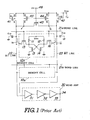
- Fig. 1 shows an example of the circuit configurations of a prior art MOS memory unit.
- the reference numeral 10 ((10A) ... (ION) ⁇ denotes static type memory cells each having a flip-flop circuit composed of two load resistors 11 and 12 and two N-channel MOS transistors 13 and 14 so as to store information by turning on or off the current.
- a memory matrix (not shown) can be configured.
- the reference numeral 21 denotes X addresses (word lines), and the numerals 22 and 23 denote a pair of complementary Y addresses (bit line and bit line).
- X decoder not shown
- MOS transistors 15, 16 in a memory cell 10A connected to the selected word line 21A are turned on to activate the memory cell 10A.
- the determined memory cell l0A is activated to permit reading or writing of information.
- the reference numeral 30 denotes an entire read amplifier.
- the bit line 22 and the bit line 23 are connected to a first-stage differential amplifier 31 of the read amplifier 30.
- An output of this differential amplifier 31 is amplified to a desired voltage level by a driving-stage inversion amplifier 32 and an output-stage buffer amplifier 33 and then outputted through an output terminal 34.
- Diode-connected N-channel MOS transistors 41 and 42 are clampers serving also as active loads of the flip-flop circuit 10A, each drain and each gate of which are connected to a power supply terminal T and each source of which is connected respectively to the bit line 22 and the bit line 23.
- Each source and each drain of precharging N-channel MOS transistors 43 and 43 are connected in parallel with each source and each drain of the MOS transistors 41 and 42, respectively.
- the source and drain of an equalizing N-channel MOS transistor 45 are connected between two intermediate junction points P and Q, that is, between the bit line 22 and the bit line 23.
- the gates of each of the three MOS transistors 43, 44 and 45 are all connected to a clock input terminal 46.
- the prior-art MOS memory as shown in Fig. 1 operates as follows:
- the word line 21A, the bit line 22 and bit line 23 are selected by an X decoder and a Y decoder (both of which are not shown). By this step, the MOS transistors 15 and 16 in the memory cell 10A are turned on.
- a clock 0 E as shown in Fig. 2(B) formed by an address transition detector (not shown) in response to the address input shown in Fig. 2(A) is supplied to the clock input terminal 46.
- the clock ⁇ E changes to an "H" (high) voltage level
- the precharging N-channel MOS transistors 43 and 44 and the equalizing N-channel MOS transistor 45 are all turned on, because each gate thereof reaches the power supply voltage V DD .
- the equalizing MOS transistor 45 has a fairly high turn-on resistance, so that the transistor 45 cannot perfectly short the bit line 22 and the bit line 23. Therefore, in the prior-art example shown in Fig. 1, current is passed through the precharging MOS transistor 43 or 44 to equalize the potentials of the bit line 22 and the bit line 23.
- this potential is assumed to be VEL.
- the absorption current I B flows into the bit line 22 through the active load-clamping MOS transistor 41.
- the clamping characteristic of the MOS transistor 41 is not so sharp as that of a bipolar transistor, the potential of the bit line 22 begins to drop to a value V L obtained by dividing the supply voltage V DD through an equivalent resistance voltage divider composed of the MOS transistors 13, 15, and 41. The speed of the voltage drop is dependent upon the stray capacitance C 22 and the equivalent resistance voltage divider.
- the voltage difference between points P and Q is amplified by the differential amplifier 31 of the read amplifier 30 and outputted from the output terminal 34 through the inversion amplifier 32 and the buffer amplifier 33.
- the output of the read amplifier 30 is the data from the memory cell 10 as shown in Fig. 2(C). It is preferable that the time Tac from when an address is determined to when data is read (access time) is as short as possible.
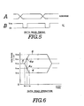
- the potentials of the bit line 22 and the bit line 23, that is, at the points P and Q are both at V EL as shown by the solid line 1 in Fig. 6.
- the potential at point P drops generally at a predetermined proportion as shown by the dot-dashed lines 2.
- the data is read from the memory cell 10A beginning from the time t 2 corresponding to a point 2a where the potential at point P reaches a predetermined reference potential V R .
- the transition time interval in order to shorten the access time, it is preferable to shorten the transition time interval; in other words, to hasten the time point 4a (t 1 ) at which the potential at point P reaches the reference potential V R by changing the transition chracteristic from a gentle slope as shown by the dot-dashed line 2 in Fig. 3 to a sharp slope as shown by the solid line 4 in Fig. 3.
- the MOS transistors 41 and 42 both function as active loads for the bit line 22 and the bit line 23 and further operate as clamping circuits.
- this condition is contradictory to the condition such that it is necessary to increase the load resistance in order to shorten the access time.
- the areas of the two MOS transistors 41 and 42 have been determined to be twice, for instance, larger than those of the precharging and equalizing MOS transistors 43 to 45 by compromising the above two contradictory conditions.
- the P-N junction capacitance (diffusion capacitance) between the N-type diffusion layer and the substrate of the memory cell 10A included in the stray capacitances C 22 and C 23 of the bit line 22 and the bit line 23 is large, thus causing the other problem such that the charge/discharge time interval is long, thus preventing a high speed operation.
- Fig. 4 shows a circuit diagram of the embodiment according to the present invention.
- many sections or elements of this embodiment are the same in function as those described in the prior-art bit line driver with reference to Fig. 1 except five MOS transistors. Therefore, the same reference numerals have been retained for similar parts which have the same functions, without making any detailed description of them.
- the sources of two P-channel MOS transistors 51 and 52 which are diode-connected by respectively connecting the gate and the drain of each of the transistors 51 and 52, are connected to the power supply terminal T .
- the source and the drain of two P-channel MOS transistors 53 and 54 having a grounded gate are connected in parallel.
- the bit line 22 and the bit line 23 are connected to the junction points R and S, respectively, between each drain of the two transistors 51 and 53 or 54 and 52, respectively.
- the source and the drain of an equalizing P-channel MOS transistor 55 are connected between the junction points R and S, and the gate of the MOS transistor 55 is connected to the clock input terminal 56.
- each area of the clamping MOS transistors 51 and 52 is determined to be three times, for instance, greater than that of the active-load MOS transistors 53 and 54 and the equalizing MOS transistor 55.
- the remaining circuit configuration of Fig. 4, other than the above, is the same as the prior art driver shown in Fig. 1.
- the operation of the embodiment is as follows: First, an assumption is made that the initial condition in the memory cell 10A is the same as that of the prior-art case, and further that the potential -of the bit line 22 is between the supply voltage V DD and the grounded potential and that of the bit line 23 is equal to the supply voltage V DD .
- a clock ⁇ E as shown in Fig. 5(B) is generated by an address transition detector (not shown), and this clock ⁇ E is supplied from the input terminal 56 to the gate of the equalizing MOS transistor 55. If the clock changes to an "L" voltage level, since the gate of the P-channel MOS transistor 55 is at the grounded potential, the transistor 55 is turned on.
- the source and the drain potentials of the equalizing MOS transistor 55 at points P and S are about 4.5V, if the supply voltage V DD is 5V, for instance, because of the influence of the threshold voltage Vth of the diode-connected P-channel MOS transistors 51 and 52 as described later. Therefore, the on-resistance of the equalizing MOS transistor 55 is sufficiently low, and it is possible to perfectly short between the bit line 22 and the bit line 23 without providing such a precharging MOS transistor as in the prior art driver. Further, the potentials of the bit line 22 and the bit line 23 are the same value V EQ as shown by the solid line 5 in Fig. 6.
- the equalizing MOS transistor 55 is turned off, because the gate voltage thereof rises up to the supply voltage V DD' releasing the connection between the bit line 22 and the bit line 23. Since the MOS transistor 14 in the memory cell 10A is off, no absorption current I B flows into the bit line 23, the stray capacitance C 23 being charged through the active load MOS transistor 54. Therefore, the potential of the bit line 23 rises up to the supply voltage V DD as shown by the solid line 6 in Fig. 6, reaching a predetermined reference potential V RT at time T l , as shown by point 6a in Fig. 6.
- the bit line 22 and the bit line 23 are connected to the supply voltage terminal T P through clamping MOS transistors 51 and 52 having a relatively large area, respectively. Therefore, when the voltage drop of the active-load MOS transistor 53 or 54 due to the absorption current I B or I B flowing into the memory cell 10 is about to exceed the threshold voltage Vth of the clamping MOS transistor 51 or 52, a large current flows through the MOS transistor 51 or 52, the potential at point R or S is sharply clamped at a predetermined clamp voltage V CH . Therefore, the equalized level V EQ of the present embodiment is a mean value of the supply voltage VDD and the clamp voltage V CH . In the case where the supply voltage V DD is 5V, for instance, the clamp voltage V CH is about 4V and therefore the equalized level V EQ is about 4.5V.
- the constants of each MOS transistor 51 to 54 can be determined independently from each other with respect to the already-mentioned two contradictory conditions of sharp clamping characteristics and high load resistance. Thus, it is possible to readily realize an optimum characteristic suitable for high speed operation.
- the P-channel MOS transistors 51 and 52 are used for the clamping transistors, the potential of the bit line 22 and the bit line 23 in equalizing operation, that is, the equalize level V EQ is sufficiently high without being subjected to the influence of the substrate effect as in the prior art driver. Therefore, the on-resistance of the equalizing MOS transistor 55 can be reduced to a sufficiently low value, without a need for special precharging MOS transistors. This allows the load of the clock amplifier to be light, so that it is possible to obtain an accurate clock signal without a use of a high power amplifier and yet realize a stable operation.
- the diffusion capacitance included in the stray capacitances C22 and C 23 of the bit line 22 and the bit bit line 23 is small, thus allowing the driver to be more advantageous to a high-speed operation.
- the P-channel clamping MOS transistors (51, 52) and the active-load transistors (53, 54) are provided separately, it is possible to obtain a bit line driver which can realize optimum characteristics readily, reduce the access time, eliminate the precharging MOS transistors, and drive bit lines stably in response to a low power clock pulse.
Abstract
Description
- The present invention relates generally to a bit line driver for a static read only memory of a microcomputer and more specifically to a bit line driver connected between a pair of complementary bit lines and having equalizing MOS transistors.
- Conventionally, MOS memory units with a number of memory cells composed of MOS transistors arranged so as to write or read information in accordance with any given and selected addresses have widely been used as a storage device for an electronic computer. In order to shorten the access time of the MOS memory, it is necessary to increase the load resistance. However, as usual, since two MOS transistors are connected as active loads so as to function as a clamper, in order to obtain good clamping characteristics, it is necessary to sufficiently decrease the inner resistance of the two MOS transistors. In other words, two contradictory conditions have been required for a prior-art bit line driver in a MOS memory unit. Further, there exists another problem in that a high output clock amplifier is required to effect a precharge operation and equalization operations simultaneously. Furthermore, there exist the other drawbacks such that the stray capacitance of the bit lines is relatively great, causing a long discharge time and thereby preventing high speed operation.
- The arrangement and operation of the prior art bit line driver for a MOS memory unit will be described in further detail with reference to the attached drawings in the detailed description of the preferred embodiment.
- With these problems in mind thereof, it is a primary object of the present invention to provide a bit line driver which can solve the above-mentioned two contradictory conditions by use of a low output clock amplifier while increasing the operation speed.
- To achieve the above-mentioned- object, in a bit line driver connected between a pair of complementary bit lines and having an equalizing MOS transistor for effecting equalization operation by shorting a pair of the complementary bit lines in response to a clock pulse applied to a gate of the MOS transistor, the driver according to the present invention comprises: (a) a pair of active-load MOS transistors, each connected between one of the complementary bit lines and a power supply, each gate of said active-load MOS transistor being connected to ground; and (b) a pair of clamping MOS transistors each connected in parallel to one of said active-load MOS transistors, each of the clamping MOS transistors being diode connected. When the equalizing MOS transistor, the two active-load MOS transistors and the two clamping MOS transistors are all of the P-channel type, each drain of the two active-load P-channel MOS transistors is connected to one of a pair of the complementary bit lines; each source of the two active-load P-channel MOS transistors is connected to the power supply; and each drain and each source of the two clamping P-channel MOS transistors are connected in parallel to each drain and each source of said two active-load P-channel MOS transistors. Further, the area of the clamping MOS transistors is determined to be about three times greater than that of the active-load MOS transistors and the equalizing MOS transistor.
- An increase in area of the clamping MOS transistors decreases the internal resistance thereof, so that the clamping operation can be improved, while a decrease in area of the active-load MOS transistors increases the internal resistance thereof, so that the access time can be improved. In summary, according to the present invention, a high load resistance and a sharp clamping characteristic are obtained simultaneously. Further, the driver operates stably on the basis of a low power clock pulse.
- The features and advantages of the bit line driver according to the present invention over the prior art bit line driver will be more clearly appreciated from the following description of the preferred embodiment of the invention taken in conjunction with the accompanying drawings in which like reference numerals designate the same elements or sections throughout the figures thereof and in which:
- Fig. 1 is a schematic block diagram showing a prior-art bit line driver;
- Fig. 2 is a waveform diagram showing the data read timing for assistance in explaining the operation of the prior-art bit line driver shown in Fig. 1;
- Fig. 3 is a graphical representation showing the data read operation for assistance in explaining the operation of the prior-art bit line driver shown in Fig.
- Fig. 4 is a schematic block diagram showing the bit line driver according to the present invention;
- Fig. 5 is a waveform diagram showing the data read timing for assistance in explaining the operation of the bit line driver shown in Fig. 4; and
- Fig. 6 is a graphical representation showing the data read operation for assistance in explaining the operation of the bit line driver shown in Fig. 4.
- To facilitate understanding of the present invention, a reference will first be made to a prior-art bit line driver, with reference to the attached drawings.
- Fig. 1 shows an example of the circuit configurations of a prior art MOS memory unit. In Fig. 1, the reference numeral 10 ((10A) ... (ION)} denotes static type memory cells each having a flip-flop circuit composed of two
load resistors 11 and 12 and two N-channel MOS transistors - The reference numeral 21 (21A ... 21N) denotes X addresses (word lines), and the
numerals MOS transistors bit line 22 and thebit line 23 are also selected by a Y decoder (not shown), the determined memory cell l0A is activated to permit reading or writing of information. - The
reference numeral 30 denotes an entire read amplifier. Thebit line 22 and thebit line 23 are connected to a first-stagedifferential amplifier 31 of theread amplifier 30. An output of thisdifferential amplifier 31 is amplified to a desired voltage level by a driving-stage inversion amplifier 32 and an output-stage buffer amplifier 33 and then outputted through anoutput terminal 34. - Diode-connected N-
channel MOS transistors bit line 22 and thebit line 23. Each source and each drain of precharging N-channel MOS transistors MOS transistors channel MOS transistor 45 are connected between two intermediate junction points P and Q, that is, between thebit line 22 and thebit line 23. The gates of each of the threeMOS transistors - The prior-art MOS memory as shown in Fig. 1 operates as follows:
- First, an assumption is made that one
MOS transistor 13 of the flip-flop in the memory cell 10A is on and theother MOS transistor 14 is off. Since the gates of the active load-clampingMOS transistors transistors bit line 22 is being charged up through theMOS transistor 41. - In response to address inputs as shown in Fig. 2(A), the word line 21A, the
bit line 22 andbit line 23 are selected by an X decoder and a Y decoder (both of which are not shown). By this step, theMOS transistors - A
clock 0 E as shown in Fig. 2(B) formed by an address transition detector (not shown) in response to the address input shown in Fig. 2(A) is supplied to the clock input terminal 46. When the clock φE changes to an "H" (high) voltage level, the precharging N-channel MOS transistors channel MOS transistor 45 are all turned on, because each gate thereof reaches the power supply voltage VDD. - In this case, if the supply voltage VDD is 5V, for instance, the potential at the points P and Q, that is, at the source and the drain of the equalizing
MOS transistor 45 is as low as about 3.2V, because of the influence of the threshold voltage ΔVth of the diode-connected N-channel MOS transistors MOS transistor 45 has a fairly high turn-on resistance, so that thetransistor 45 cannot perfectly short thebit line 22 and thebit line 23. Therefore, in the prior-art example shown in Fig. 1, current is passed through theprecharging MOS transistor bit line 22 and thebit line 23. Here, this potential is assumed to be VEL. - When the clock φE changes to an "L" (low) voltage level, since each gate voltage of the
MOS transistors 43 to 45 drops down to the ground potential, theseMOS transistors 43 to 45 are all turned off. Since theMOS transistor 14 in the memory cell 10A is off, the potential of thebit line 23 released from the connection with thebit line 22 is held at a constant level VEL due to the influence of the threshold voltage Vth of theMOS transistor 42 and the substrate effect Δ Vth. - On the other hand, since the
MOS transistors bit line 22 through the active load-clampingMOS transistor 41. Here, since the clamping characteristic of theMOS transistor 41 is not so sharp as that of a bipolar transistor, the potential of thebit line 22 begins to drop to a value VL obtained by dividing the supply voltage VDD through an equivalent resistance voltage divider composed of theMOS transistors - When the potential of the
bit line 22 reaches a predetermined potential VCL higher than the above-mentioned VL, the voltage drop stops due to the clamping operation of theMOS transistor 41. In the case where the supply voltage VDD is 5V, for instance, this clamped voltage VCL is about 2.6V. - As described above, the voltage difference between points P and Q is amplified by the
differential amplifier 31 of theread amplifier 30 and outputted from theoutput terminal 34 through theinversion amplifier 32 and thebuffer amplifier 33. In this case, the output of theread amplifier 30 is the data from the memory cell 10 as shown in Fig. 2(C). It is preferable that the time Tac from when an address is determined to when data is read (access time) is as short as possible. - Once the data is read from the memory cell 10A, the clock 0E is applied to the terminal 46, in the same way as previously stated, the potential at point P is restored from VCL to VEL, and the data output disappears as shown in Fig. 2(C).
- The relationship between the operation and the access time of the prior-art MOS memory as shown in Fig. 1 now will further be described with reference to Fig. 3.
- As already described, during the period in which the clock φE is at an "H" voltage level, the potentials of the
bit line 22 and thebit line 23, that is, at the points P and Q are both at VEL as shown by the solid line 1 in Fig. 6. From the time to when the clock φE changes to an "L" voltage level, the potential at point P drops generally at a predetermined proportion as shown by the dot-dashedlines 2. During this transition time interval, the data is read from the memory cell 10A beginning from the time t2 corresponding to a point 2a where the potential at point P reaches a predetermined reference potential VR. - Therefore, in order to shorten the access time, it is preferable to shorten the transition time interval; in other words, to hasten the time point 4a (t1) at which the potential at point P reaches the reference potential VR by changing the transition chracteristic from a gentle slope as shown by the dot-dashed
line 2 in Fig. 3 to a sharp slope as shown by thesolid line 4 in Fig. 3. - In the case where the voltage changes according to the time as described above, since V=IR; that is, dv/dt = R.dI/dt, the gradient of the voltage change characteristic is dependent upon the resistance value and the current change rate (the degree of change in current per unit time). Therefore, it is possible to shorten the access time by increasing the load resistance.
- In the prior-art bit line driver as shown in Fig. 1, however, the
MOS transistors bit line 22 and thebit line 23 and further operate as clamping circuits. In order to permit a preferable clamping operation, it is necessary to increase the area of theMOS transistors MOS transistors MOS transistors 43 to 45 by compromising the above two contradictory conditions. However, there still exists a problem in that it is basically very difficult to determine transistor constants so as to obtain these preferable characteristics while taking the above-mentioned two contradictory conditions into consideration. - Further, in the prior art driver, since the three
MOS transistors - Furthermore, in the prior art driver, since the potential of the
bit line 22 and thebit line 23 is as low as VEL = 2.3V, the P-N junction capacitance (diffusion capacitance) between the N-type diffusion layer and the substrate of the memory cell 10A included in the stray capacitances C22 and C23 of thebit line 22 and thebit line 23 is large, thus causing the other problem such that the charge/discharge time interval is long, thus preventing a high speed operation. - In view of the above description, reference is now made to an embodiment of the bit line driver according to the present invention, with reference to the attached drawings.
- Fig. 4 shows a circuit diagram of the embodiment according to the present invention. In the drawing, many sections or elements of this embodiment are the same in function as those described in the prior-art bit line driver with reference to Fig. 1 except five MOS transistors. Therefore, the same reference numerals have been retained for similar parts which have the same functions, without making any detailed description of them.
- In Fig. 4, the sources of two P-
channel MOS transistors transistors MOS transistors channel MOS transistors bit line 22 and thebit line 23 are connected to the junction points R and S, respectively, between each drain of the twotransistors clock input terminal 56. When all thetransistors 51 to 55 for clamping and equalizing operations and an active load are made up of P-channel MOS transistors, it is possible to facilitate the pattern layout inside the integrated circuit. - Further, each area of the clamping
MOS transistors load MOS transistors - The operation of the embodiment is as follows: First, an assumption is made that the initial condition in the memory cell 10A is the same as that of the prior-art case, and further that the potential -of the
bit line 22 is between the supply voltage VDD and the grounded potential and that of thebit line 23 is equal to the supply voltage VDD. - Then, in response to an address input as shown in Fig. 5(A), a clock φE as shown in Fig. 5(B) is generated by an address transition detector (not shown), and this clock φE is supplied from the
input terminal 56 to the gate of the equalizing MOS transistor 55. If the clock changes to an "L" voltage level, since the gate of the P-channel MOS transistor 55 is at the grounded potential, the transistor 55 is turned on. - In this embodiment, the source and the drain potentials of the equalizing MOS transistor 55 at points P and S are about 4.5V, if the supply voltage VDD is 5V, for instance, because of the influence of the threshold voltage Vth of the diode-connected P-
channel MOS transistors bit line 22 and thebit line 23 without providing such a precharging MOS transistor as in the prior art driver. Further, the potentials of thebit line 22 and thebit line 23 are the same value VEQ as shown by thesolid line 5 in Fig. 6. - During the non-equalization time interval, since the clock φE changes to an "H" voltage level, the equalizing MOS transistor 55 is turned off, because the gate voltage thereof rises up to the supply voltage VDD' releasing the connection between the
bit line 22 and thebit line 23. Since theMOS transistor 14 in the memory cell 10A is off, no absorption current IB flows into thebit line 23, the stray capacitance C23 being charged through the activeload MOS transistor 54. Therefore, the potential of thebit line 23 rises up to the supply voltage VDD as shown by thesolid line 6 in Fig. 6, reaching a predetermined reference potential VRT at time Tl, as shown bypoint 6a in Fig. 6. - On the other hand, since the
MOS transistors bit line 22 through the activeload MOS transistor 53. As described above, since the area of thisMOS transistor 53 is determined to be relatively small, the equivalent resistance value is relatively high. Therefore, the potential of thebit line 22 drops sharply as shown by thesolid line 4 in Fig. 6, reaching a predetermined reference potential VRB at time tl, as shown by point 4a in Fig. 6. - Therefore, a data signal rising sharply and a data signal falling sharply are generated in the
bit line 22 and thebit line 23, respectively, as shown by thesolid lines - Further, in this embodiment, as already described, the
bit line 22 and thebit line 23 are connected to the supply voltage terminal TP through clampingMOS transistors load MOS transistor MOS transistor MOS transistor - Further, when data "0" is written in the memory cell 10A, the potential of the
bit line 22 or thebit line 23 is driven to near the ground potential by a writing drive amplifier (not shown). In order to start the read operation immediately after this, it is necessary to recover the potential of thebit line 22 and thebit line 23 to the equalize level VEQ (write recovery). In the present embodiment, however, since there are provided clampingMOS transistors - As described above, in the present invention, since there are provided active-
load MOS transistors MOS transistors MOS transistor 51 to 54 can be determined independently from each other with respect to the already-mentioned two contradictory conditions of sharp clamping characteristics and high load resistance. Thus, it is possible to readily realize an optimum characteristic suitable for high speed operation. - Further, in the present embodiment, since the P-
channel MOS transistors bit line 22 and thebit line 23 in equalizing operation, that is, the equalize level VEQ is sufficiently high without being subjected to the influence of the substrate effect as in the prior art driver. Therefore, the on-resistance of the equalizing MOS transistor 55 can be reduced to a sufficiently low value, without a need for special precharging MOS transistors. This allows the load of the clock amplifier to be light, so that it is possible to obtain an accurate clock signal without a use of a high power amplifier and yet realize a stable operation. - Furthermore, in this embodiment, since the equalize level VEQ is high as described above, the diffusion capacitance included in the stray capacitances C22 and C23 of the
bit line 22 and the bit bitline 23 is small, thus allowing the driver to be more advantageous to a high-speed operation. - As described above, according to the present invention, since the P-channel clamping MOS transistors (51, 52) and the active-load transistors (53, 54) are provided separately, it is possible to obtain a bit line driver which can realize optimum characteristics readily, reduce the access time, eliminate the precharging MOS transistors, and drive bit lines stably in response to a low power clock pulse.
Claims (7)
Applications Claiming Priority (2)
| Application Number | Priority Date | Filing Date | Title |
|---|---|---|---|
| JP60077953A JPS61237290A (en) | 1985-04-12 | 1985-04-12 | Bit line drive circuit |
| JP77953/85 | 1985-04-12 |
Publications (2)
| Publication Number | Publication Date |
|---|---|
| EP0201733A2 true EP0201733A2 (en) | 1986-11-20 |
| EP0201733A3 EP0201733A3 (en) | 1988-07-20 |
Family
ID=13648371
Family Applications (1)
| Application Number | Title | Priority Date | Filing Date |
|---|---|---|---|
| EP86104982A Ceased EP0201733A3 (en) | 1985-04-12 | 1986-04-11 | Bit line driver |
Country Status (4)
| Country | Link |
|---|---|
| US (1) | US4802128A (en) |
| EP (1) | EP0201733A3 (en) |
| JP (1) | JPS61237290A (en) |
| KR (1) | KR950001423B1 (en) |
Cited By (2)
| Publication number | Priority date | Publication date | Assignee | Title |
|---|---|---|---|---|
| EP0429018A2 (en) * | 1989-11-17 | 1991-05-29 | Nec Corporation | Semiconductor memory device having input/output data signal lines propagating data bit at high-speed regardless of fluctuation in power voltage signal |
| EP0459297A2 (en) * | 1990-05-28 | 1991-12-04 | Nec Corporation | Semiconductor memory device having transfer gate array associated with monitoring circuit for bit line pair |
Families Citing this family (11)
| Publication number | Priority date | Publication date | Assignee | Title |
|---|---|---|---|---|
| JPS62273694A (en) * | 1986-05-22 | 1987-11-27 | Sony Corp | Sense amplifier |
| JPS6446288A (en) * | 1987-08-13 | 1989-02-20 | Toshiba Corp | Semiconductor memory device |
| JP2690554B2 (en) * | 1989-05-08 | 1997-12-10 | 日本電気アイシーマイコンシステム株式会社 | Semiconductor memory device |
| JPH0660665A (en) * | 1992-08-10 | 1994-03-04 | Nec Corp | Bit line load circuit of semiconductor static ram |
| KR950005577B1 (en) * | 1992-12-30 | 1995-05-25 | 현대전자산업주식회사 | Bit line load circuit |
| JPH07130177A (en) * | 1993-11-02 | 1995-05-19 | Nec Corp | Semiconductor storage device |
| US5687130A (en) * | 1994-11-30 | 1997-11-11 | Texas Instruments Incorporated | Memory cell with single bit line read back |
| EP0929896B1 (en) * | 1996-09-30 | 2001-11-28 | Advanced Micro Devices, Inc. | Memory including resistor bit-line loads |
| US7471588B2 (en) * | 2006-05-05 | 2008-12-30 | Altera Corporation | Dual port random-access-memory circuitry |
| US8619464B1 (en) | 2011-08-26 | 2013-12-31 | Altera Corporation | Static random-access memory having read circuitry with capacitive storage |
| TWI618075B (en) * | 2012-11-06 | 2018-03-11 | 半導體能源研究所股份有限公司 | Semiconductor device and driving method thereof |
Citations (5)
| Publication number | Priority date | Publication date | Assignee | Title |
|---|---|---|---|---|
| US4112506A (en) * | 1976-10-07 | 1978-09-05 | Sharp Kabushiki Kaisha | Random access memory using complementary field effect devices |
| EP0121208A2 (en) * | 1983-03-30 | 1984-10-10 | Kabushiki Kaisha Toshiba | Static type semiconductor memory circuit |
| US4479202A (en) * | 1979-09-13 | 1984-10-23 | Tokyo Shibaura Denki Kabushiki Kaisha | CMOS Sense amplifier |
| US4494221A (en) * | 1982-03-03 | 1985-01-15 | Inmos Corporation | Bit line precharging and equilibrating circuit |
| EP0136811A2 (en) * | 1983-09-21 | 1985-04-10 | THORN EMI North America Inc. | Bit line load and column circuitry for a semiconductor memory |
Family Cites Families (1)
| Publication number | Priority date | Publication date | Assignee | Title |
|---|---|---|---|---|
| US4355377A (en) * | 1980-06-30 | 1982-10-19 | Inmos Corporation | Asynchronously equillibrated and pre-charged static ram |
-
1985
- 1985-04-12 JP JP60077953A patent/JPS61237290A/en active Pending
-
1986
- 1986-04-10 US US06/849,962 patent/US4802128A/en not_active Expired - Lifetime
- 1986-04-11 EP EP86104982A patent/EP0201733A3/en not_active Ceased
- 1986-04-12 KR KR1019860002794A patent/KR950001423B1/en not_active IP Right Cessation
Patent Citations (5)
| Publication number | Priority date | Publication date | Assignee | Title |
|---|---|---|---|---|
| US4112506A (en) * | 1976-10-07 | 1978-09-05 | Sharp Kabushiki Kaisha | Random access memory using complementary field effect devices |
| US4479202A (en) * | 1979-09-13 | 1984-10-23 | Tokyo Shibaura Denki Kabushiki Kaisha | CMOS Sense amplifier |
| US4494221A (en) * | 1982-03-03 | 1985-01-15 | Inmos Corporation | Bit line precharging and equilibrating circuit |
| EP0121208A2 (en) * | 1983-03-30 | 1984-10-10 | Kabushiki Kaisha Toshiba | Static type semiconductor memory circuit |
| EP0136811A2 (en) * | 1983-09-21 | 1985-04-10 | THORN EMI North America Inc. | Bit line load and column circuitry for a semiconductor memory |
Cited By (4)
| Publication number | Priority date | Publication date | Assignee | Title |
|---|---|---|---|---|
| EP0429018A2 (en) * | 1989-11-17 | 1991-05-29 | Nec Corporation | Semiconductor memory device having input/output data signal lines propagating data bit at high-speed regardless of fluctuation in power voltage signal |
| EP0429018A3 (en) * | 1989-11-17 | 1992-09-30 | Nec Corporation | Semiconductor memory device having input/output data signal lines propagating data bit at high-speed regardless of fluctuation in power voltage signal |
| EP0459297A2 (en) * | 1990-05-28 | 1991-12-04 | Nec Corporation | Semiconductor memory device having transfer gate array associated with monitoring circuit for bit line pair |
| EP0459297A3 (en) * | 1990-05-28 | 1992-10-21 | Nec Corporation | Semiconductor memory device having transfer gate array associated with monitoring circuit for bit line pair |
Also Published As
| Publication number | Publication date |
|---|---|
| KR950001423B1 (en) | 1995-02-24 |
| JPS61237290A (en) | 1986-10-22 |
| KR860008562A (en) | 1986-11-17 |
| EP0201733A3 (en) | 1988-07-20 |
| US4802128A (en) | 1989-01-31 |
Similar Documents
| Publication | Publication Date | Title |
|---|---|---|
| US4616342A (en) | Semiconductor memory device | |
| KR100382687B1 (en) | Power-on reset circuit for an integrated circuit memory | |
| US4750155A (en) | 5-Transistor memory cell which can be reliably read and written | |
| US3440444A (en) | Driver-sense circuit arrangement | |
| US3993917A (en) | Parameter independent FET sense amplifier | |
| US5243573A (en) | Sense amplifier for nonvolatile semiconductor storage devices | |
| JPH0241113B2 (en) | ||
| US4813022A (en) | Static memory with pull-up circuit for pulling-up a potential on a bit line | |
| KR950001126B1 (en) | Memory circuit | |
| US4112512A (en) | Semiconductor memory read/write access circuit and method | |
| US4802128A (en) | Bit line driver | |
| US5640355A (en) | Semiconductor memory device | |
| EP0050529A2 (en) | Semiconductor memory circuit | |
| EP0598400A2 (en) | Semiconductor memory device | |
| US4338679A (en) | Row driver circuit for semiconductor memory | |
| US4131951A (en) | High speed complementary MOS memory | |
| JPH03272087A (en) | Semiconductor storage device | |
| JP2845212B2 (en) | Semiconductor storage device | |
| US4760559A (en) | Semiconductor memory device | |
| US4815040A (en) | Static memory using a MIS field effect transistor | |
| US5544097A (en) | SRAM memory cell with reduced internal cell voltage | |
| US5949730A (en) | Method and apparatus for quickly restoring digit I/O lines | |
| GB2056209A (en) | Memory device | |
| JPH0785358B2 (en) | Semiconductor memory device | |
| EP0318094B1 (en) | Integrated memory circuit with on-chip supply voltage control |
Legal Events
| Date | Code | Title | Description |
|---|---|---|---|
| PUAI | Public reference made under article 153(3) epc to a published international application that has entered the european phase |
Free format text: ORIGINAL CODE: 0009012 |
|
| AK | Designated contracting states |
Kind code of ref document: A2 Designated state(s): DE FR GB NL |
|
| PUAL | Search report despatched |
Free format text: ORIGINAL CODE: 0009013 |
|
| RHK1 | Main classification (correction) |
Ipc: G11C 7/00 |
|
| AK | Designated contracting states |
Kind code of ref document: A3 Designated state(s): DE FR GB NL |
|
| 17P | Request for examination filed |
Effective date: 19890119 |
|
| 17Q | First examination report despatched |
Effective date: 19890602 |
|
| STAA | Information on the status of an ep patent application or granted ep patent |
Free format text: STATUS: THE APPLICATION HAS BEEN REFUSED |
|
| 18R | Application refused |
Effective date: 19900305 |
|
| RIN1 | Information on inventor provided before grant (corrected) |
Inventor name: WATANABE, KAZUO Inventor name: KOHRI, SHUMPEI Inventor name: ARAKI, SHIGEO |